Lecture 29 Random Access Memory RAM 1 Random



- Slides: 34

Lecture 29 Random Access Memory (RAM) 1

Random Access Memory (RAM) A memory unit is a collection of storage cells together with associated circuits needed to transfer information in and out of the device. Memory cells can be accessed for information transfer to or from any desired random location and hence the name Random Access Memory, abbreviated as RAM 2

Overview ° Memory is a collection of storage cells with associated input and output circuitry • Possible to read and write cells ° Random access memory (RAM) contains words of information ° Data accessed using a sequence of signals • Leads to timing waveforms ° Decoders are an important part of memories • Selects specific data in the RAM ° Static RAM loses values when circuit power is removed. 3

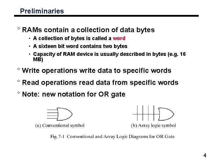
Preliminaries ° RAMs contain a collection of data bytes • A collection of bytes is called a word • A sixteen bit word contains two bytes • Capacity of RAM device is usually described in bytes (e. g. 16 MB) ° Write operations write data to specific words ° Read operations read data from specific words ° Note: new notation for OR gate 4

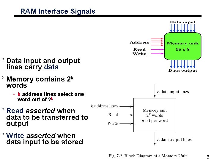
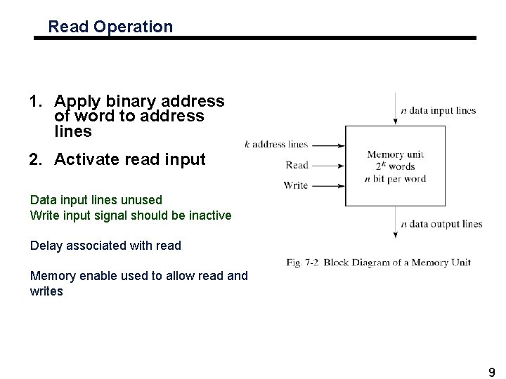
RAM Interface Signals ° Data input and output lines carry data ° Memory contains 2 k words • k address lines select one word out of 2 k ° Read asserted when data to be transferred to output ° Write asserted when data input to be stored 5

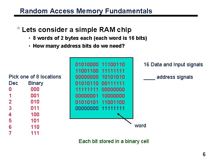
Random Access Memory Fundamentals ° Lets consider a simple RAM chip • 8 words of 2 bytes each (each word is 16 bits) • How many address bits do we need? Pick one of 8 locations Dec Binary 0 000 1 001 2 010 3 011 4 100 5 101 6 110 7 111 01010000 1100 0000 01010110 1111 00000001 0101 0000 11100110 1111 1010 00111111 0000 10000000 1100 1111 16 Data and Input signals ____ address signals word Each bit stored in a binary cell 6

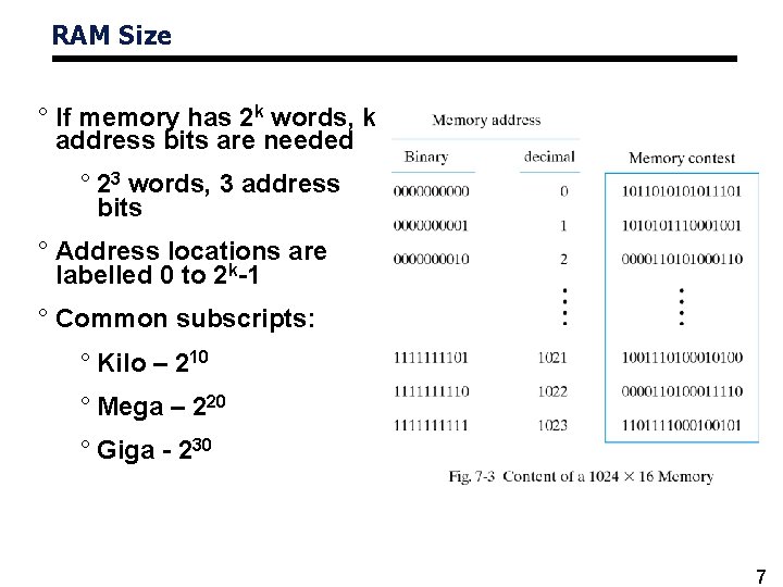
RAM Size ° If memory has 2 k words, k address bits are needed ° 23 words, 3 address bits ° Address locations are labelled 0 to 2 k-1 ° Common subscripts: ° Kilo – 210 ° Mega – 220 ° Giga - 230 7

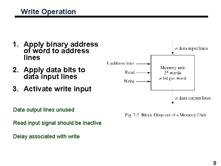
Write Operation 1. Apply binary address of word to address lines 2. Apply data bits to data input lines 3. Activate write input Data output lines unused Read input signal should be inactive Delay associated with write 8

Read Operation 1. Apply binary address of word to address lines 2. Activate read input Data input lines unused Write input signal should be inactive Delay associated with read Memory enable used to allow read and writes 9

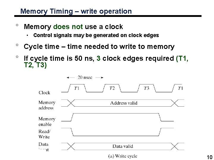
Memory Timing – write operation ° Memory does not use a clock • Control signals may be generated on clock edges ° Cycle time – time needed to write to memory ° If cycle time is 50 ns, 3 clock edges required (T 1, T 2, T 3) 10

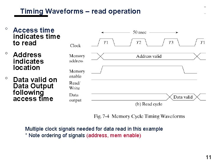
Timing Waveforms – read operation ° Access time indicates time to read ° Address indicates location ° Data valid on Data Output following access time Multiple clock signals needed for data read in this example * Note ordering of signals (address, mem enable) 11

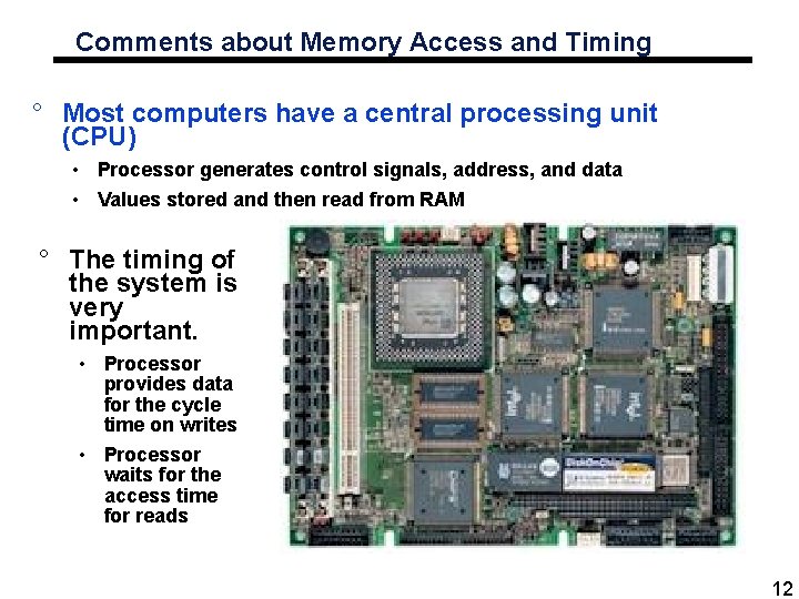
Comments about Memory Access and Timing ° Most computers have a central processing unit (CPU) • Processor generates control signals, address, and data • Values stored and then read from RAM ° The timing of the system is very important. • Processor provides data for the cycle time on writes • Processor waits for the access time for reads 12

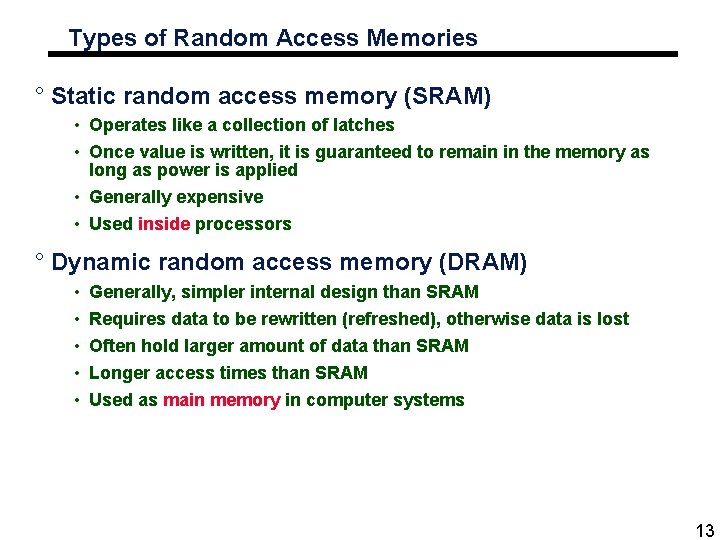
Types of Random Access Memories ° Static random access memory (SRAM) • Operates like a collection of latches • Once value is written, it is guaranteed to remain in the memory as long as power is applied • Generally expensive • Used inside processors ° Dynamic random access memory (DRAM) • • • Generally, simpler internal design than SRAM Requires data to be rewritten (refreshed), otherwise data is lost Often hold larger amount of data than SRAM Longer access times than SRAM Used as main memory in computer systems 13

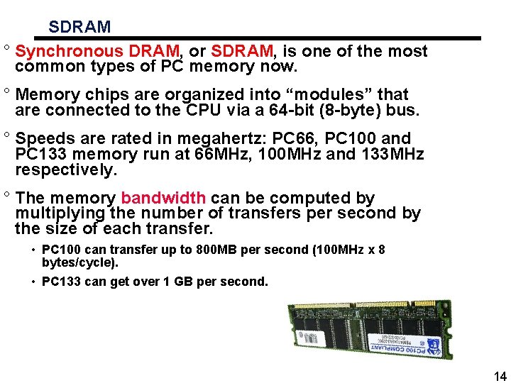
SDRAM ° Synchronous DRAM, or SDRAM, is one of the most common types of PC memory now. ° Memory chips are organized into “modules” that are connected to the CPU via a 64 -bit (8 -byte) bus. ° Speeds are rated in megahertz: PC 66, PC 100 and PC 133 memory run at 66 MHz, 100 MHz and 133 MHz respectively. ° The memory bandwidth can be computed by multiplying the number of transfers per second by the size of each transfer. • PC 100 can transfer up to 800 MB per second (100 MHz x 8 bytes/cycle). • PC 133 can get over 1 GB per second. 14

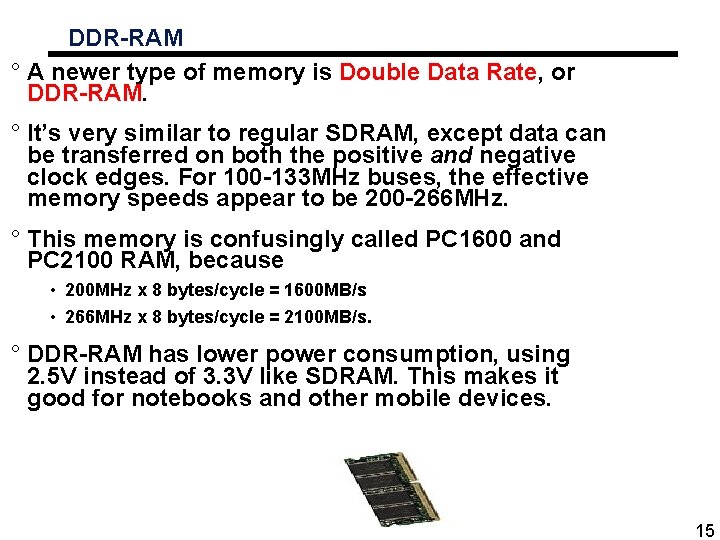
DDR-RAM ° A newer type of memory is Double Data Rate, or DDR-RAM. ° It’s very similar to regular SDRAM, except data can be transferred on both the positive and negative clock edges. For 100 -133 MHz buses, the effective memory speeds appear to be 200 -266 MHz. ° This memory is confusingly called PC 1600 and PC 2100 RAM, because • 200 MHz x 8 bytes/cycle = 1600 MB/s • 266 MHz x 8 bytes/cycle = 2100 MB/s. ° DDR-RAM has lower power consumption, using 2. 5 V instead of 3. 3 V like SDRAM. This makes it good for notebooks and other mobile devices. 15

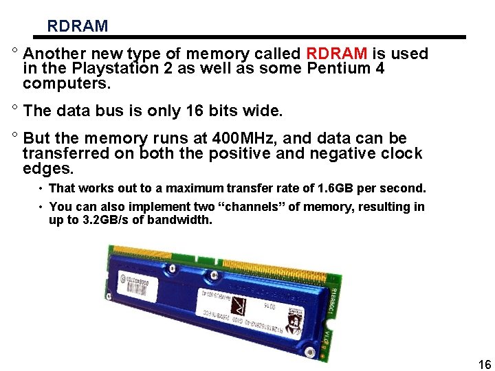
RDRAM ° Another new type of memory called RDRAM is used in the Playstation 2 as well as some Pentium 4 computers. ° The data bus is only 16 bits wide. ° But the memory runs at 400 MHz, and data can be transferred on both the positive and negative clock edges. • That works out to a maximum transfer rate of 1. 6 GB per second. • You can also implement two “channels” of memory, resulting in up to 3. 2 GB/s of bandwidth. 16

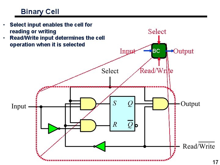
Binary Cell • Select input enables the cell for reading or writing • Read/Write input determines the cell operation when it is selected Select Input BC Output Read/Write 17

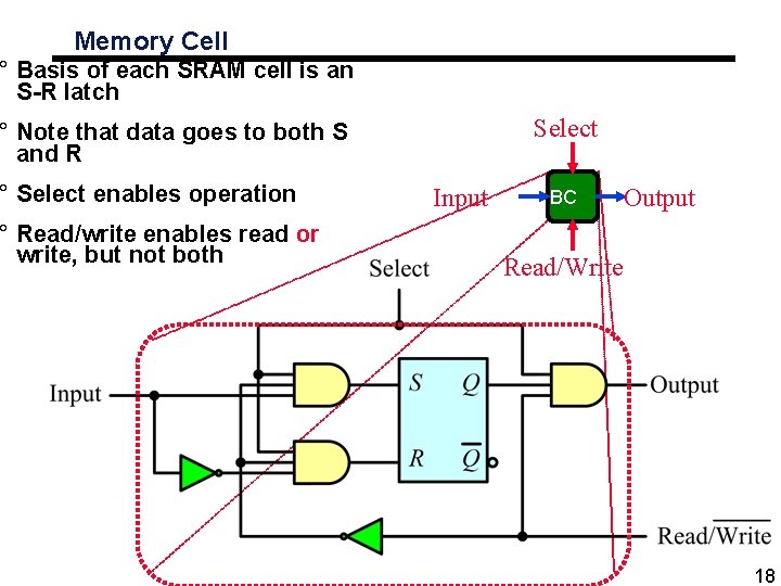
Memory Cell ° Basis of each SRAM cell is an S-R latch Select ° Note that data goes to both S and R ° Select enables operation ° Read/write enables read or write, but not both Input BC Output Read/Write 18

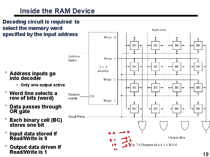
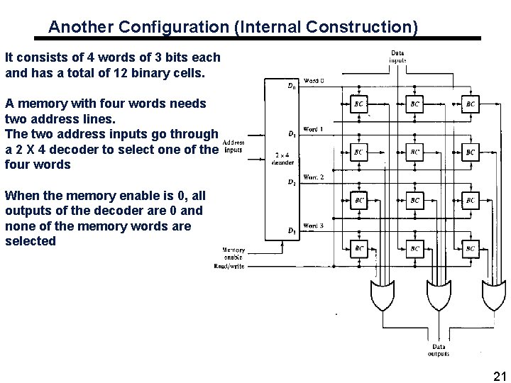
Inside the RAM Device Decoding circuit is required to select the memory word specified by the input address ° Address inputs go into decoder • Only one output active ° Word line selects a row of bits (word) ° Data passes through OR gate ° Each binary cell (BC) stores one bit ° Input data stored if Read/Write is 0 ° Output data driven if Read/Write is 1 19

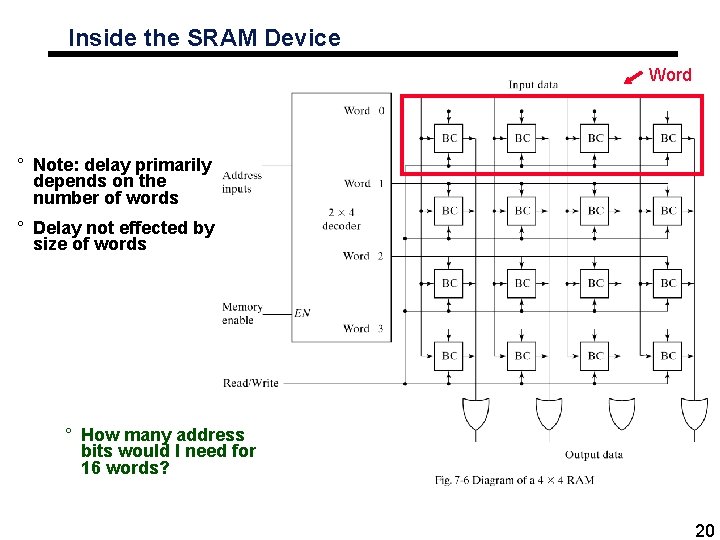
Inside the SRAM Device Word ° Note: delay primarily depends on the number of words ° Delay not effected by size of words ° How many address bits would I need for 16 words? 20

Another Configuration (Internal Construction) It consists of 4 words of 3 bits each and has a total of 12 binary cells. A memory with four words needs two address lines. The two address inputs go through a 2 X 4 decoder to select one of the four words When the memory enable is 0, all outputs of the decoder are 0 and none of the memory words are selected 21

22

Array of RAM Chips ° Integrated-circuit RAM chips are available in a variety of sizes ° If the memory unit needed for an application is larger than the capacity of one chip, it is necessary to combine a number of chips in an array to form the required memory size. ° Capacity of the memory depends on two parameters: the number of words and the number of bits per word. ° An increase in the number of words requires that we increase the address length ° Every bit added to the length of the address doubles the number of words in memory. ° The increase in the number of bits per word requires that we increase the length of the data input and output lines, but the address length remains the same. 23

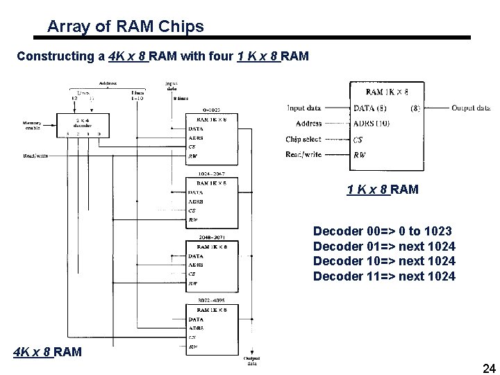
Array of RAM Chips Constructing a 4 K x 8 RAM with four 1 K x 8 RAM Decoder 00=> 0 to 1023 Decoder 01=> next 1024 Decoder 10=> next 1024 Decoder 11=> next 1024 4 K x 8 RAM 24

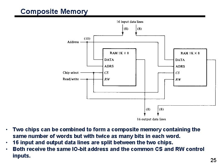
Composite Memory • Two chips can be combined to form a composite memory containing the same number of words but with twice as many bits in each word. • 16 input and output data lines are split between the two chips. • Both receive the same IO-bit address and the common CS and RW control inputs. 25

26

Error-Detection and Correcting Code ° Memory array may cause occasional errors in storing and retrieving the binary information ° Reliability of a memory unit may be improved by employing error-detecting and correcting codes Error Detection ° The most common error-detection scheme is the parity bit ° A parity bit is generated and stored along with the data word in memory. The parity of the word is checked after reading it from memory. The data word is accepted if the parity sense is correct. If the parity checked results in an inversion, an error is detected, but it cannot be corrected. 27

Error-Detection and Correcting Code Error Correction ° An error-correcting code generates multiple check bits that are stored with the data word in memory. ° Each check bit is a parity over a group of bits in the data word. ° When the word is read from memory, the associated parity bits are also read from memory and compared with a new set of check bits generated from the read data. ° If the check bits compare, it signifies that no error has occurred. If the check bits do not compare with the stored parity, they generate a unique pattern, called a syndrome, that can be used to identify the bit in error. ° A single error occurs when a bit changes in value from I to 0 or from 0 to 1 during the write or read operation ° If the specific bit in error is identified, then the error can be corrected by complementing the erroneous bit. 28

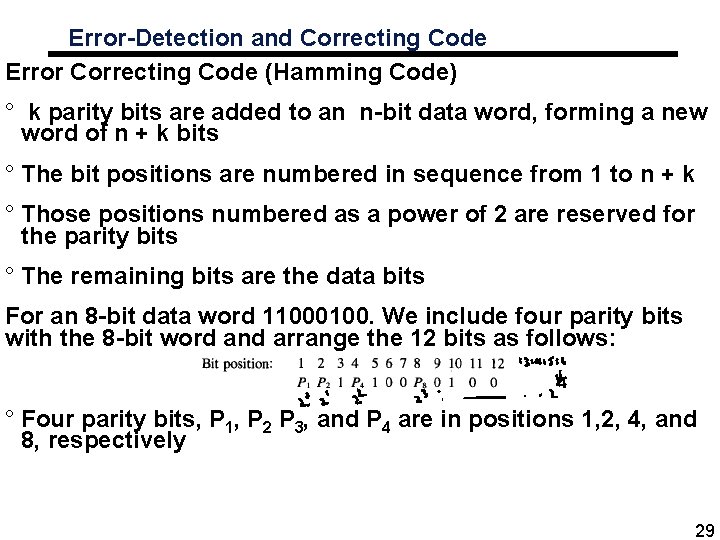
Error-Detection and Correcting Code Error Correcting Code (Hamming Code) ° k parity bits are added to an n-bit data word, forming a new word of n + k bits ° The bit positions are numbered in sequence from 1 to n + k ° Those positions numbered as a power of 2 are reserved for the parity bits ° The remaining bits are the data bits For an 8 -bit data word 11000100. We include four parity bits with the 8 -bit word and arrange the 12 bits as follows: ° Four parity bits, P 1, P 2 P 3, and P 4 are in positions 1, 2, 4, and 8, respectively 29

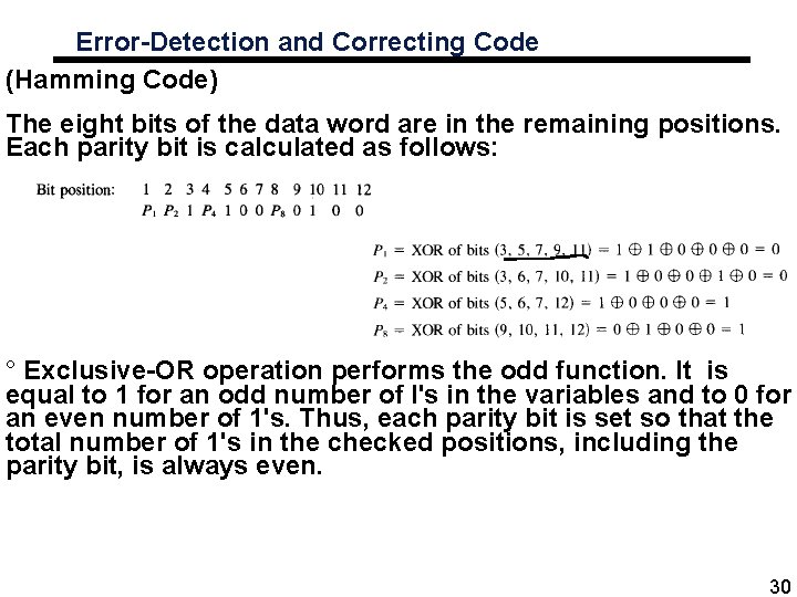
Error-Detection and Correcting Code (Hamming Code) The eight bits of the data word are in the remaining positions. Each parity bit is calculated as follows: ° Exclusive-OR operation performs the odd function. It is equal to 1 for an odd number of I's in the variables and to 0 for an even number of 1's. Thus, each parity bit is set so that the total number of 1's in the checked positions, including the parity bit, is always even. 30

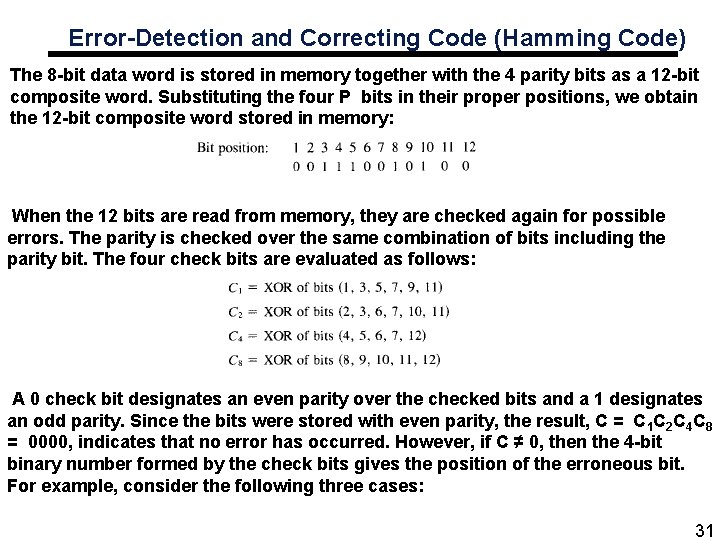
Error-Detection and Correcting Code (Hamming Code) The 8 -bit data word is stored in memory together with the 4 parity bits as a 12 -bit composite word. Substituting the four P bits in their proper positions, we obtain the 12 -bit composite word stored in memory: When the 12 bits are read from memory, they are checked again for possible errors. The parity is checked over the same combination of bits including the parity bit. The four check bits are evaluated as follows: A 0 check bit designates an even parity over the checked bits and a 1 designates an odd parity. Since the bits were stored with even parity, the result, C = C 1 C 2 C 4 C 8 = 0000, indicates that no error has occurred. However, if C ≠ 0, then the 4 -bit binary number formed by the check bits gives the position of the erroneous bit. For example, consider the following three cases: 31

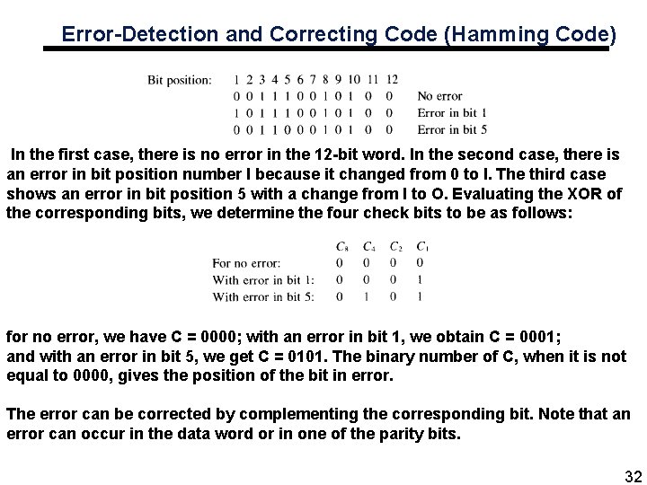
Error-Detection and Correcting Code (Hamming Code) In the first case, there is no error in the 12 -bit word. In the second case, there is an error in bit position number I because it changed from 0 to I. The third case shows an error in bit position 5 with a change from I to O. Evaluating the XOR of the corresponding bits, we determine the four check bits to be as follows: for no error, we have C = 0000; with an error in bit 1, we obtain C = 0001; and with an error in bit 5, we get C = 0101. The binary number of C, when it is not equal to 0000, gives the position of the bit in error. The error can be corrected by complementing the corresponding bit. Note that an error can occur in the data word or in one of the parity bits. 32

33

Summary ° Memories provide storage for computers ° Memories are organized in words • Selected by addresses ° SRAMs store data in latches • Accessed by surrounding circuitry ° RAM waveforms indicate the control signals needed for access ° Words in SRAMs are accessed with decoders • Only one word selected at a time ° Error correction and detection codes (Hamming) 34