Lecture 29 IEEE 1149 1 JTAG Advanced Boundary
Lecture 29 IEEE 1149. 1 JTAG Advanced Boundary Scan & Description Language (BSDL) n n n Special scan cells and pins Cell timing / wiring constraints Cell delay measurements n Boundary Scan Description Language n Summary Copyright 2001, Agrawal & Bushnell VLSI Test: Lecture 29 1
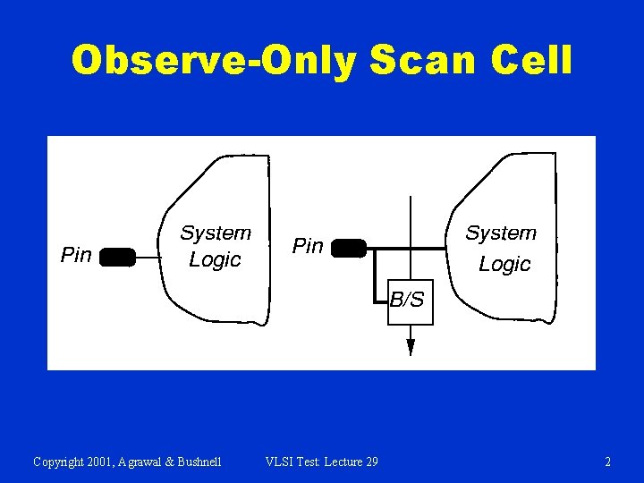
Observe-Only Scan Cell Copyright 2001, Agrawal & Bushnell VLSI Test: Lecture 29 2
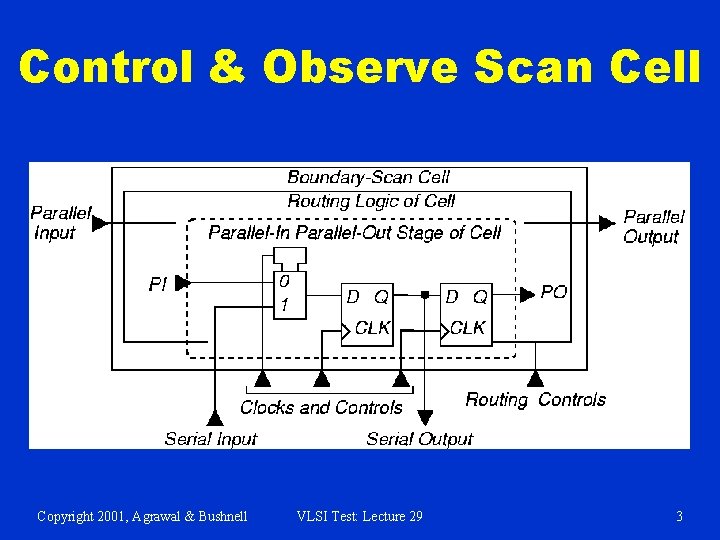
Control & Observe Scan Cell Copyright 2001, Agrawal & Bushnell VLSI Test: Lecture 29 3

Bidirectional Pins Copyright 2001, Agrawal & Bushnell VLSI Test: Lecture 29 4
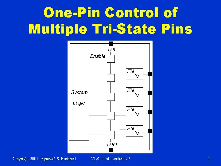
One-Pin Control of Multiple Tri-State Pins Copyright 2001, Agrawal & Bushnell VLSI Test: Lecture 29 5
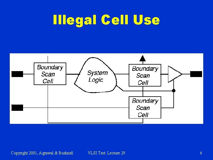
Illegal Cell Use Copyright 2001, Agrawal & Bushnell VLSI Test: Lecture 29 6
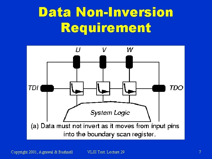
Data Non-Inversion Requirement Copyright 2001, Agrawal & Bushnell VLSI Test: Lecture 29 7
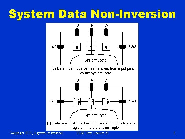
System Data Non-Inversion Copyright 2001, Agrawal & Bushnell VLSI Test: Lecture 29 8
Cell Delay Constraints n n Delay between falling TCK edge and changes at component output pins may be skewed § May need to avoid simultaneous output switching to save power or avoid burnout Scan register cells with latched parallel outputs § May be reset to either logic 0 or 1 n When Test-Logic-Reset TAP controller state entered n On first falling TCK edge in Test-Logic. Reset state Copyright 2001, Agrawal & Bushnell VLSI Test: Lecture 29 9
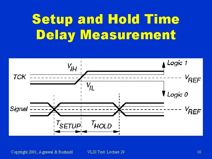
Setup and Hold Time Delay Measurement Copyright 2001, Agrawal & Bushnell VLSI Test: Lecture 29 10

Propagation Delay Measurement Method Copyright 2001, Agrawal & Bushnell VLSI Test: Lecture 29 11
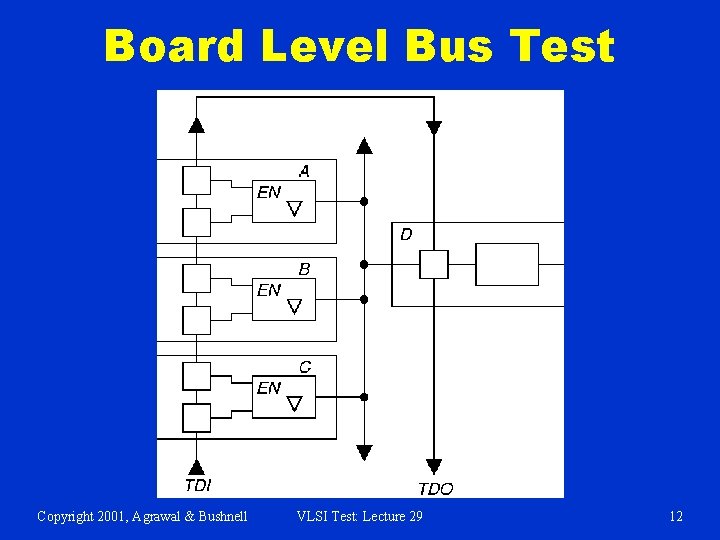
Board Level Bus Test Copyright 2001, Agrawal & Bushnell VLSI Test: Lecture 29 12
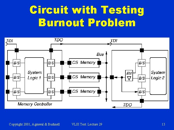
Circuit with Testing Burnout Problem Copyright 2001, Agrawal & Bushnell VLSI Test: Lecture 29 13
Purpose of Boundary Scan Description Language (BSDL) n n Facilitate communication of information describing test logic of parts: § Between companies and CAD tools § Used by automatic test-pattern generators § Used by synthesis tools to synthesize test logic Not usable as a simulation model Cannot describe voltages, currents, or timing Implemented as subset of VHDL § Must modify for certain VHDL tools Copyright 2001, Agrawal & Bushnell VLSI Test: Lecture 29 14
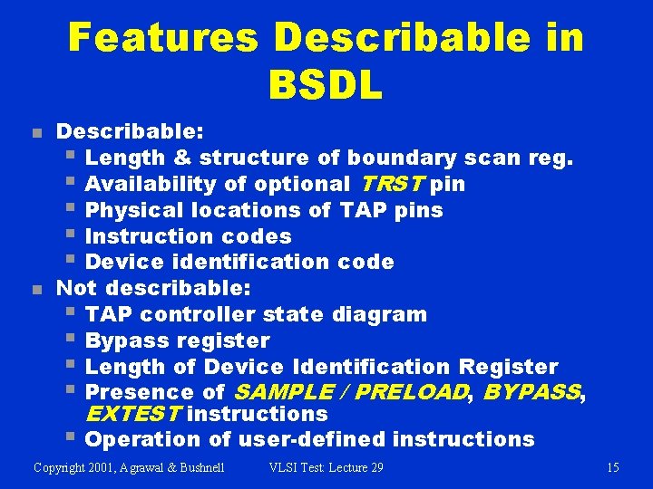
Features Describable in BSDL n n Describable: § Length & structure of boundary scan reg. § Availability of optional TRST pin § Physical locations of TAP pins § Instruction codes § Device identification code Not describable: § TAP controller state diagram § Bypass register § Length of Device Identification Register § Presence of SAMPLE / PRELOAD, BYPASS, EXTEST instructions § Operation of user-defined instructions Copyright 2001, Agrawal & Bushnell VLSI Test: Lecture 29 15
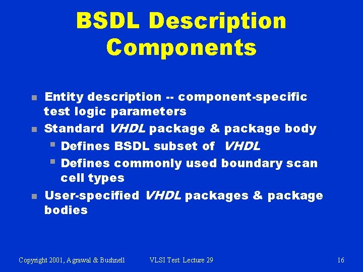
BSDL Description Components n n n Entity description -- component-specific test logic parameters Standard VHDL package & package body § Defines BSDL subset of VHDL § Defines commonly used boundary scan cell types User-specified VHDL packages & package bodies Copyright 2001, Agrawal & Bushnell VLSI Test: Lecture 29 16
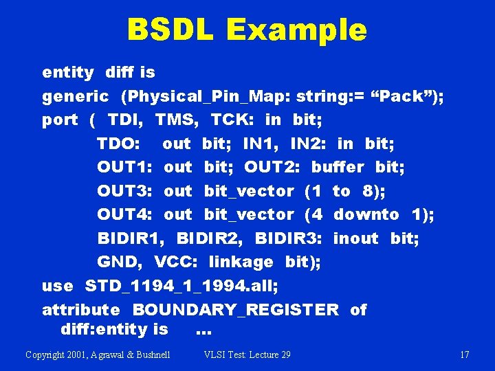
BSDL Example entity diff is generic (Physical_Pin_Map: string: = “Pack”); port ( TDI, TMS, TCK: in bit; TDO: out bit; IN 1, IN 2: in bit; OUT 1: out bit; OUT 2: buffer bit; OUT 3: out bit_vector (1 to 8); OUT 4: out bit_vector (4 downto 1); BIDIR 1, BIDIR 2, BIDIR 3: inout bit; GND, VCC: linkage bit); use STD_1194_1_1994. all; attribute BOUNDARY_REGISTER of diff: entity is. . . Copyright 2001, Agrawal & Bushnell VLSI Test: Lecture 29 17

Pin Descriptions n n Standard USE statement (required): use STD_1149_1_1994. all; PIN Types: § in (input-only) § out (may be tri-state or open-collector) § buffer (active, 2 -state, always driven) § inout (bidirectional) § linkage (power, ground, analog, non-connect) Relate logical signals to package physical pins Group ports -- differential voltage or current pairs (one signal is always complement of other) Copyright 2001, Agrawal & Bushnell VLSI Test: Lecture 29 18
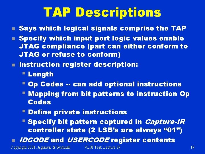
TAP Descriptions n n Says which logical signals comprise the TAP Specify which input port logic values enable JTAG compliance (part can either conform to JTAG or refuse to conform) Instruction register description: § Length § Op Codes -- can add optional instructions § Mapping from bit patterns to instruction Op Codes § Define private instructions § Specify bit pattern captured in Capture-IR controller state (2 LSB’s are always “ 01”) IDCODE and USERCODE register contents Copyright 2001, Agrawal & Bushnell VLSI Test: Lecture 29 19
Scan Cell Definitions n n Define existence and length of boundary scan register cells -- have these types: § INPUT -- control & observe, observe-only § CLOCK -- cell at clock input § OUTPUT 2 -- drives 2 -state output § OUTPUT 3 -- drivers 3 -state output § CONTROL -- controls 3 -state output § CONTROLR -- disabled in Test-Logic-Reset state § INTERNAL -- not associated with digital pin § BIDIR -- reversible cell for bidirectional pin § OBSERVE_ONLY -- single input observe-only cell Define which instructions access which registers Copyright 2001, Agrawal & Bushnell VLSI Test: Lecture 29 20
Summary n Boundary Scan Standard has become absolutely essential -§ No longer possible to test printed circuit boards with bed-of-nails tester § Not possible to test multi-chip modules at all without it § Supports BIST, external testing with Automatic Test Equipment, and boundary scan chain reconfiguration as BIST pattern generator and response compacter § Now getting widespread usage Copyright 2001, Agrawal & Bushnell VLSI Test: Lecture 29 21
- Slides: 21