Lecture 22 Chapters 3 Logic Circuits Part 1
- Slides: 39

Lecture 22 Chapters 3 Logic Circuits Part 1

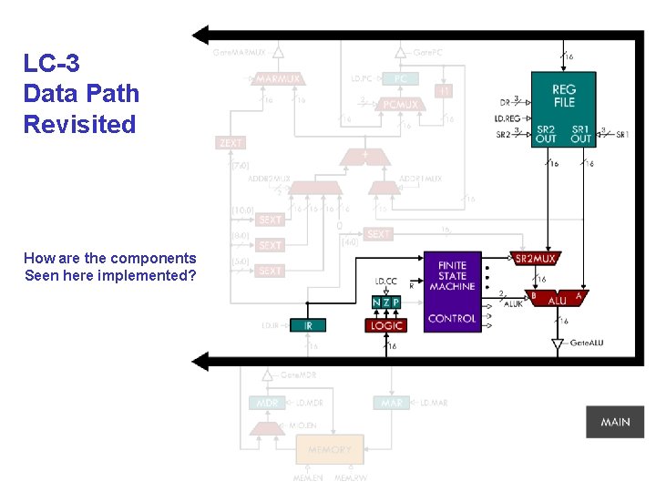
LC-3 Data Path Revisited How are the components Seen here implemented?

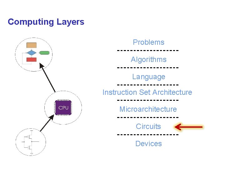
Computing Layers Problems Algorithms Language Instruction Set Architecture Microarchitecture Circuits Devices

How do we represent data in a computer? At the lowest level, a computer is an electronic machine. • works by controlling the flow of electrons Easy to recognize two conditions: 1. presence of a voltage – we’ll call this state “ 1” 2. absence of a voltage – we’ll call this state “ 0” Could base state on value of voltage, but control and detection circuits more complex. • compare turning on a light switch to measuring or regulating voltage

Transistor: Building Block of Computers Logically, each transistor acts as a switch Combined to implement logic functions (gates) • AND, OR, NOT Combined to build higher-level structures • Adder, multiplexer, decoder, register, memory … • Adder, multiplier … Combined to build simple processor • LC-3 More in-depth information about this section of the class can be found in MIT’s Open Courseware videos on You. Tube, search MIT 6. 004 Spring 2016. Lectures 1 through 6 cover material we will learn about

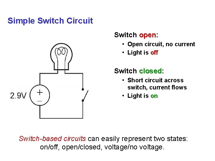
Simple Switch Circuit Switch open: open • Open circuit, no current • Light is off Switch closed: closed • Short circuit across switch, current flows • Light is on Switch-based circuits can easily represent two states: on/off, open/closed, voltage/no voltage.

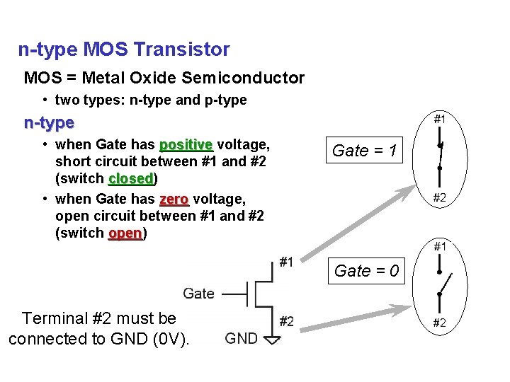
n-type MOS Transistor MOS = Metal Oxide Semiconductor • two types: n-type and p-type n-type • when Gate has positive voltage, short circuit between #1 and #2 (switch closed) closed • when Gate has zero voltage, open circuit between #1 and #2 (switch open) open Gate = 1 Gate = 0 Terminal #2 must be connected to GND (0 V).

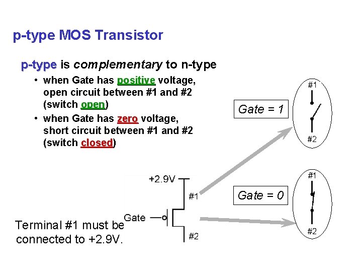
p-type MOS Transistor p-type is complementary to n-type • when Gate has positive voltage, open circuit between #1 and #2 (switch open) open • when Gate has zero voltage, short circuit between #1 and #2 (switch closed) closed Gate = 1 Gate = 0 Terminal #1 must be connected to +2. 9 V.

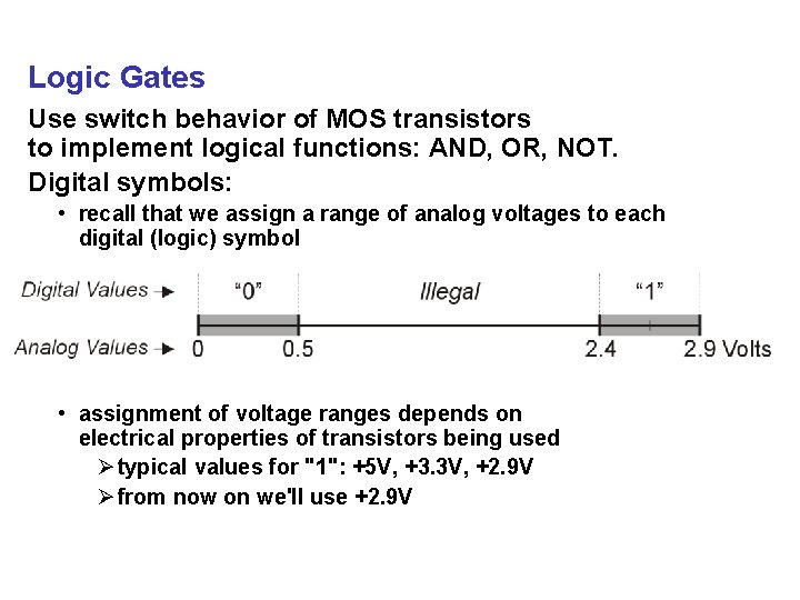
Logic Gates Use switch behavior of MOS transistors to implement logical functions: AND, OR, NOT. Digital symbols: • recall that we assign a range of analog voltages to each digital (logic) symbol • assignment of voltage ranges depends on electrical properties of transistors being used Ø typical values for "1": +5 V, +3. 3 V, +2. 9 V Ø from now on we'll use +2. 9 V

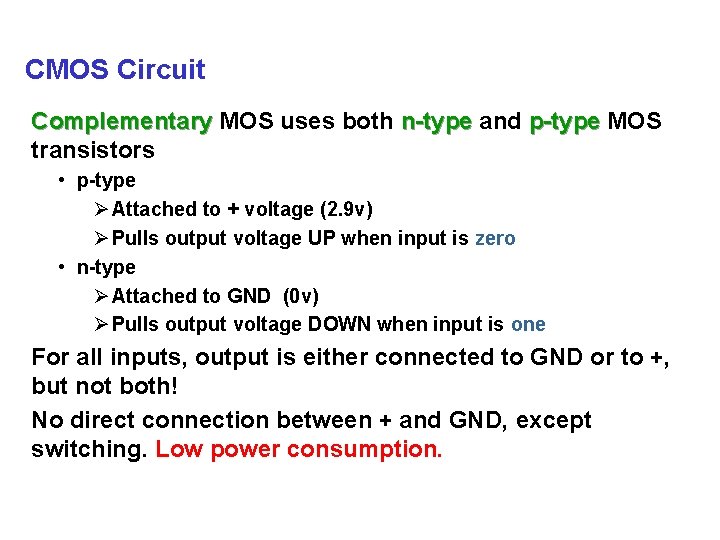
CMOS Circuit Complementary MOS uses both n-type and p-type MOS transistors • p-type Ø Attached to + voltage (2. 9 v) Ø Pulls output voltage UP when input is zero • n-type Ø Attached to GND (0 v) Ø Pulls output voltage DOWN when input is one For all inputs, output is either connected to GND or to +, but not both! No direct connection between + and GND, except switching. Low power consumption.

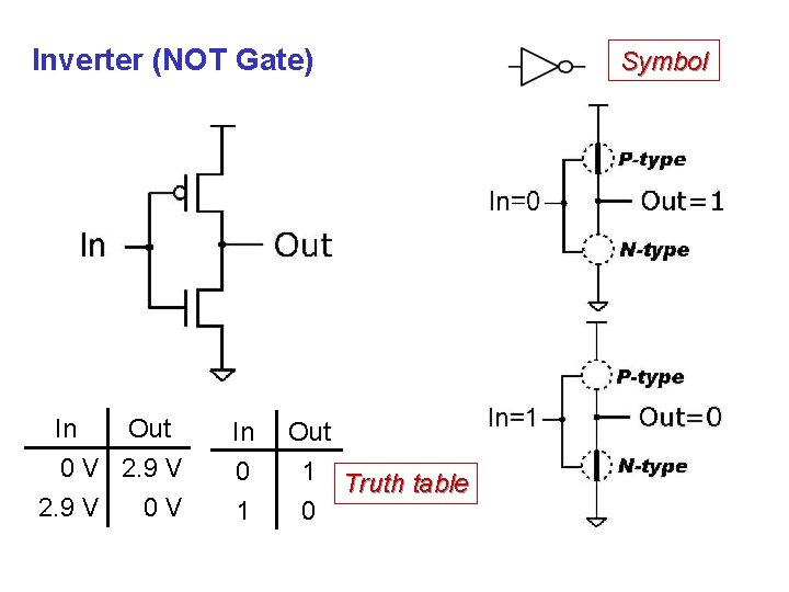
Inverter (NOT Gate) In Out 0 V 2. 9 V 0 V In 0 1 Out 1 Truth table 0 Symbol

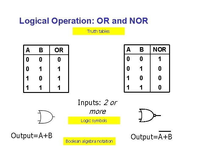
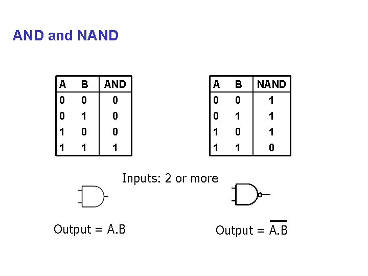
Logical Operation: OR and NOR Truth tables A B OR A B NOR 0 0 0 1 1 0 1 0 1 1 0 0 1 1 1 0 Inputs: 2 or more Logic symbols Output=A+B Boolean algebra notation Output=A+B

AND and NAND A B NAND 0 0 0 1 1 1 0 0 1 1 1 1 0 Inputs: 2 or more Output = A. B

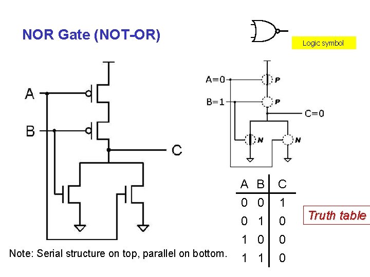
NOR Gate (NOT-OR) Logic symbol A 0 0 1 Note: Serial structure on top, parallel on bottom. B 0 1 0 C 1 0 0 1 1 0 Truth table

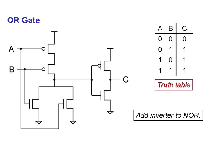
OR Gate A 0 0 1 B 0 1 0 C 0 1 1 1 Truth table Add inverter to NOR.

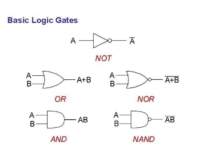
Basic Logic Gates

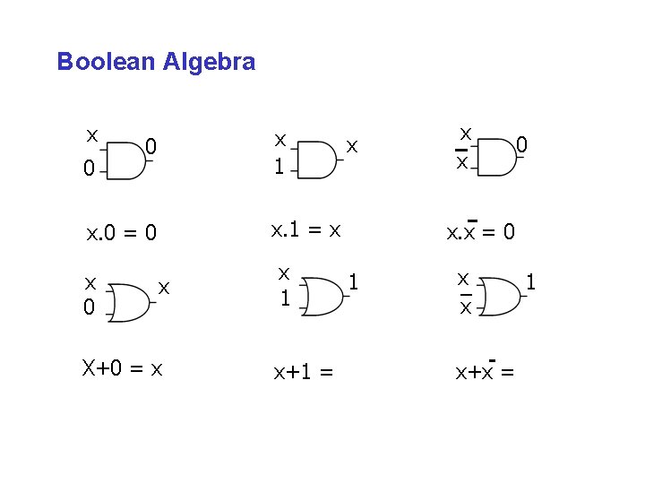
Boolean Algebra x 0 x 1 0 x. 1 = x x. 0 = 0 x x X+0 = x x 1 x+1 = x x 0 x. x = 0 1 x x x+x = 1

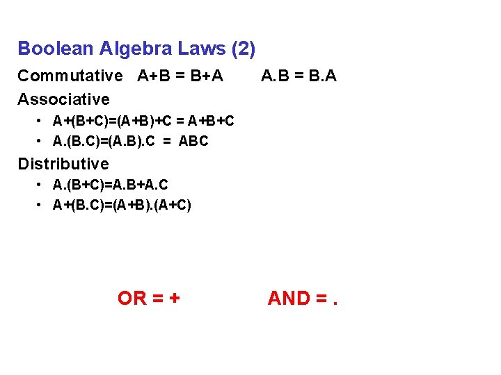
Boolean Algebra Laws (2) Commutative A+B = B+A Associative A. B = B. A • A+(B+C)=(A+B)+C = A+B+C • A. (B. C)=(A. B). C = ABC Distributive • A. (B+C)=A. B+A. C • A+(B. C)=(A+B). (A+C) OR = + AND =.

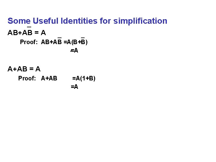
Some Useful Identities for simplification AB+AB = A Proof: AB+AB =A(B+B) =A A+AB = A Proof: A+AB =A(1+B) =A

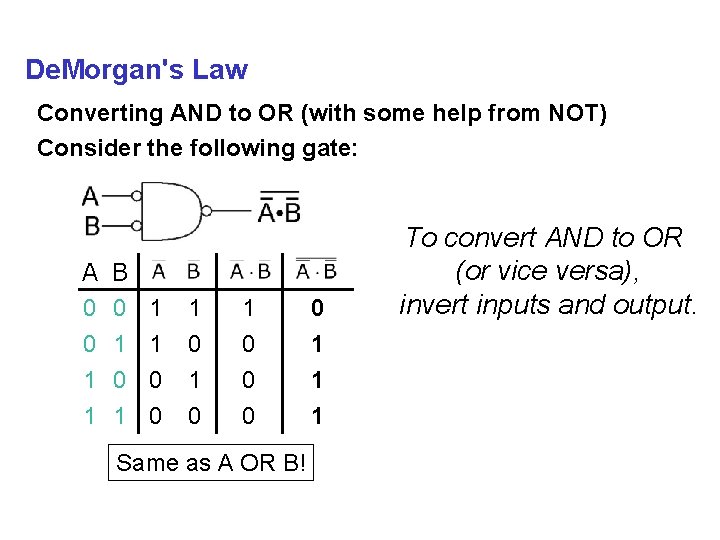
De. Morgan's Law Converting AND to OR (with some help from NOT) Consider the following gate: A 0 0 1 B 0 1 1 1 0 0 1 1 0 0 0 1 1 0 0 1 Same as A OR B! To convert AND to OR (or vice versa), invert inputs and output.

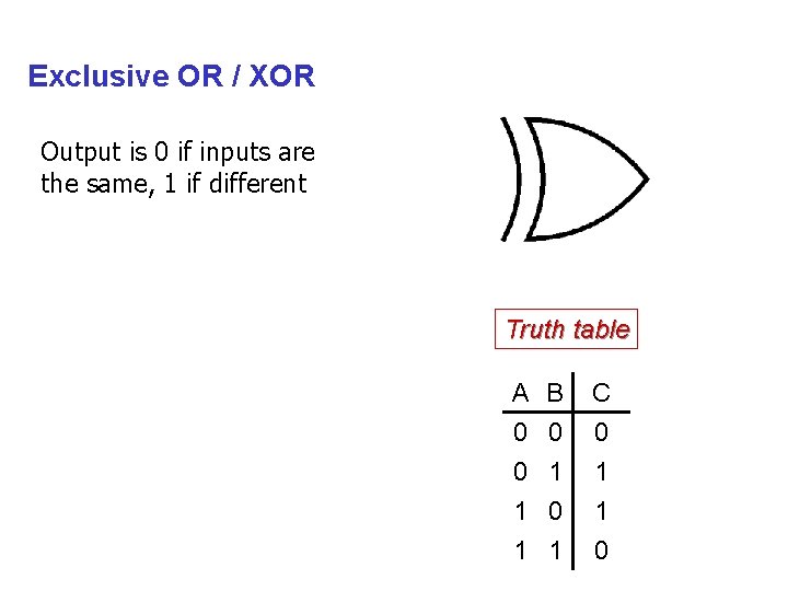
Exclusive OR / XOR Output is 0 if inputs are the same, 1 if different Truth table A 0 0 1 B 0 1 0 C 0 1 1 0

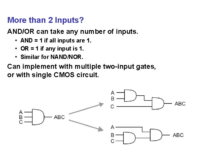
More than 2 Inputs? AND/OR can take any number of inputs. • AND = 1 if all inputs are 1. • OR = 1 if any input is 1. • Similar for NAND/NOR. Can implement with multiple two-input gates, or with single CMOS circuit.

Propagation Delay • Each gate has a propagation delay, typically fraction of a nanosecond (10 -9 sec). • Delays add depending on the chain of gates the signals have to go trough. • Clock frequency is determined by the delay of the longest combinational path between storage elements. Measured in GHz (109 cycles per sec).

Building Functions from Logic Gates Combinational Logic Circuit • output depends only on the current inputs • stateless Sequential Logic Circuit • output depends on the sequence of inputs (past and present) • stores information (state) from past inputs We'll first look at some useful combinational circuits, then show to use sequential circuits to store information.

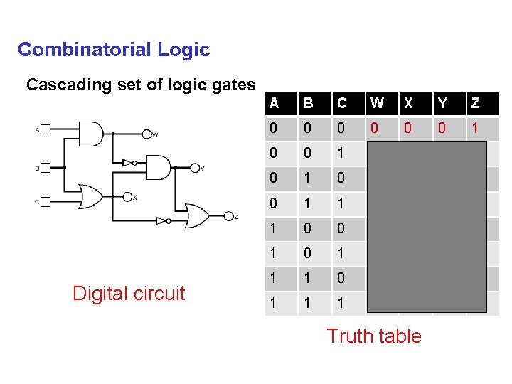
Combinatorial Logic Cascading set of logic gates Digital circuit A B C W X Y Z 0 0 0 1 1 1 0 0 1 1 1 0 0 0 1 1 1 0 1 1 0 0 1 1 1 0 0 Truth table

Functional Blocks Decoder Multiplexer Full Adder Any general function

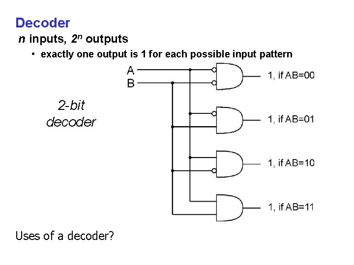
Decoder n inputs, 2 n outputs • exactly one output is 1 for each possible input pattern 2 -bit decoder Uses of a decoder?

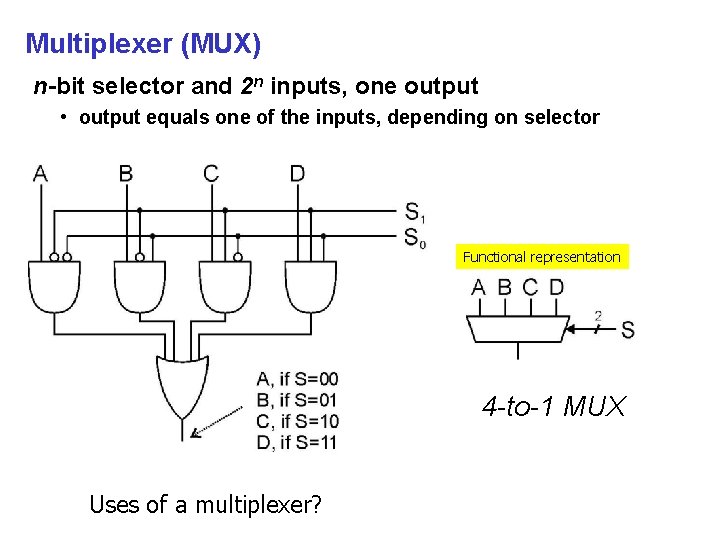
Multiplexer (MUX) n-bit selector and 2 n inputs, one output • output equals one of the inputs, depending on selector Functional representation 4 -to-1 MUX Uses of a multiplexer?

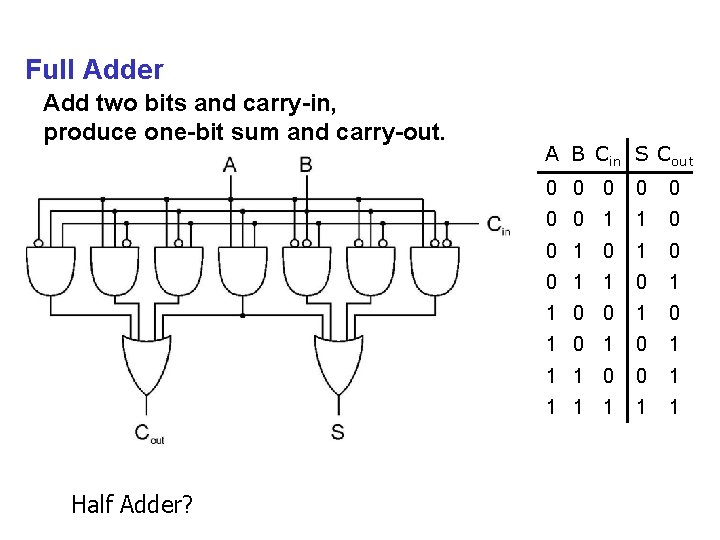
Full Adder Add two bits and carry-in, produce one-bit sum and carry-out. Half Adder? A B Cin S Cout 0 0 0 0 1 1 0 0 1 0 1 1 1 0 0 1 1 1

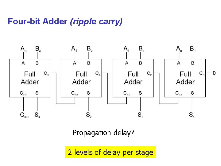
Four-bit Adder (ripple carry) Propagation delay? 2 levels of delay per stage

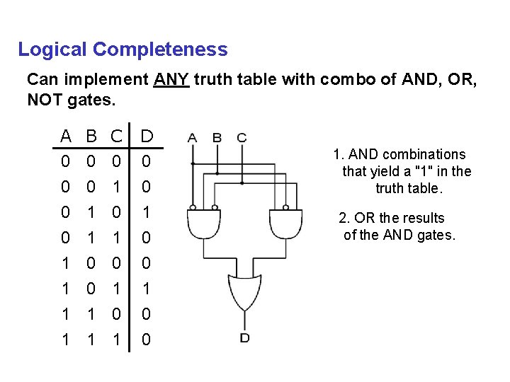
Logical Completeness Can implement ANY truth table with combo of AND, OR, NOT gates. A 0 0 0 B 0 0 1 1 1 0 0 1 1 C D 0 0 1 1 0 0 1. AND combinations that yield a "1" in the truth table. 2. OR the results of the AND gates.

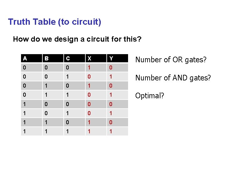
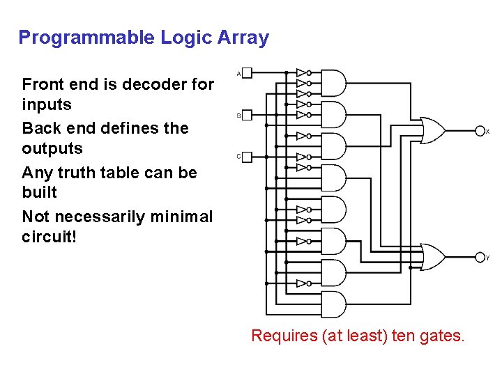
Truth Table (to circuit) How do we design a circuit for this? A B C X Y 0 0 0 1 0 1 0 1 0 0 1 0 1 0 1 1 1 1 1 Number of OR gates? Number of AND gates? Optimal?

Programmable Logic Array Front end is decoder for inputs Back end defines the outputs Any truth table can be built Not necessarily minimal circuit! Requires (at least) ten gates.

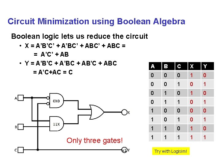
Circuit Minimization using Boolean Algebra Boolean logic lets us reduce the circuit • X = A’B’C’ + A’BC’ + ABC = = A’C’ + AB • Y = A’B’C + A’BC + AB’C + ABC = A’C+AC = C Only three gates! A B C X Y 0 0 0 1 0 1 0 1 0 0 1 0 1 0 1 1 1 1 1 Try with Logisim!

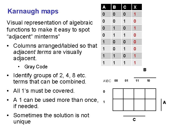
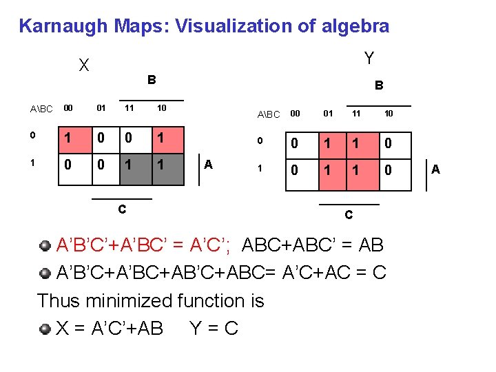
Karnaugh maps Visual representation of algebraic functions to make it easy to spot “adjacent” minterms” • Columns arranged/labled so that adjacent terms are visually adjacent. • Gray Code • Identify groups of 2, 4, 8 etc. terms that can be combined. A B C X 0 0 0 1 0 1 1 0 0 0 1 0 1 1 1 1 1 B ABC • All 1’s must be covered. 0 • A 1 can be used more than once, if needed. 1 • Sometimes the solution is not unique 00 01 11 10 A C

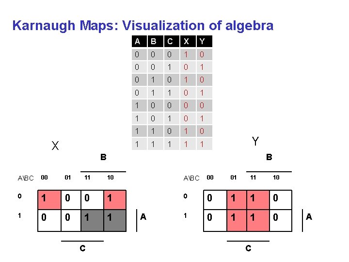
Karnaugh Maps: Visualization of algebra X A B C X Y 0 0 0 1 0 1 0 1 0 0 1 0 1 0 1 1 1 1 1 Y B B ABC 00 01 11 10 0 1 1 0 0 1 1 1 0 C A

Karnaugh Maps: Visualization of algebra Y X B B ABC 00 01 11 10 0 1 1 C A ABC 00 01 11 10 0 0 1 1 0 C A’B’C’+A’BC’ = A’C’; ABC+ABC’ = AB A’B’C+A’BC+AB’C+ABC= A’C+AC = C Thus minimized function is X = A’C’+AB Y = C A

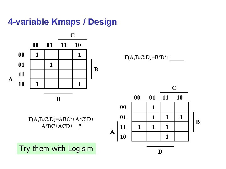
4 -variable Kmaps / Design C 00 00 11 1 01 A 01 10 1 1 B 11 10 F(A, B, C, D)=B’D’+_____ 1 1 C 00 D F(A, B, C, D)=ABC’+A’C’D+ A’BC+ACD+ ? Try them with Logisim A 01 11 10 1 01 1 1 11 1 10 1 D B

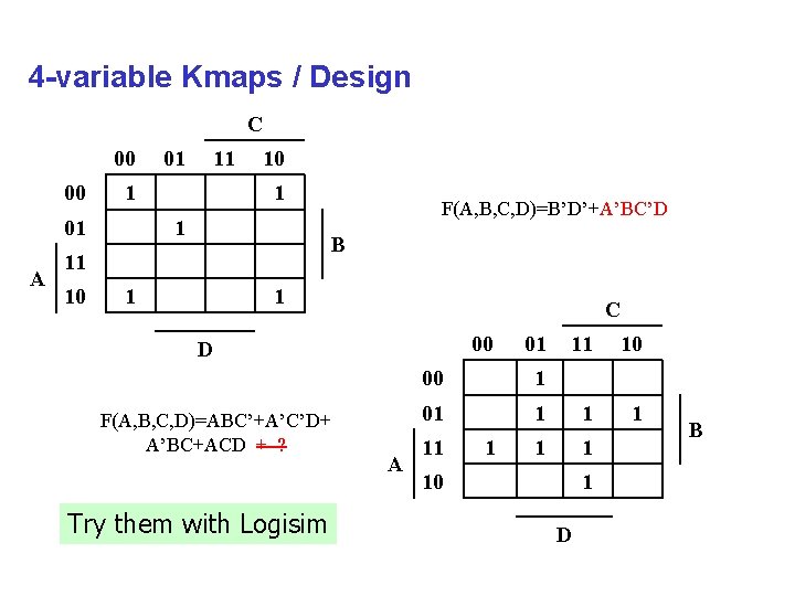
4 -variable Kmaps / Design C 00 00 11 1 01 A 01 10 1 1 B 11 10 F(A, B, C, D)=B’D’+A’BC’D 1 1 C 00 D F(A, B, C, D)=ABC’+A’C’D+ A’BC+ACD + ? Try them with Logisim A 01 11 10 1 01 1 1 11 1 10 1 D B