Lecture 22 Chapter 4 Surface Characterization in Biomaterials
Lecture 22: Chapter 4: Surface Characterization in Biomaterials and Tissue Engineering Really just a bunch of Microscopy. November 14, 2005 EEBE 512/ENEL 619. 15 Dr. KE Jones
It’s from the Greek, mikros (small) and skopeo (look at). November 14, 2005 EEBE 512/ENEL 619. 15 Dr. KE Jones

Objectives n n Starting from the de Broglie equation, demonstrate that TEM resolution depends on the voltage of the accelerating field Describe the principle and sample preparation for: ¨ TEM, SEM, 2 modes of STM & SFM, XPS, AES, SIMS, ISS, FT-IR, ATR, FTIR-ATR November 14, 2005 EEBE 512/ENEL 619. 15 Dr. KE Jones
Outline November 14, 2005 EEBE 512/ENEL 619. 15 Dr. KE Jones
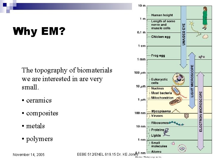
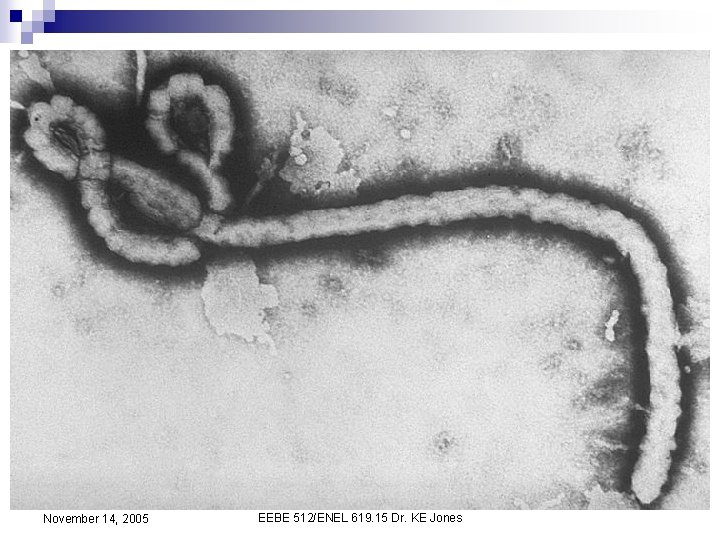
Why EM? The topography of biomaterials we are interested in are very small. • ceramics • composites • metals • polymers November 14, 2005 EEBE 512/ENEL 619. 15 Dr. KE Jones
November 14, 2005 EEBE 512/ENEL 619. 15 Dr. KE Jones
Why electrons? It all started with light, but even with better lenses, oil immersion and short wavelengths, resolution was only about 0. 2 mm/1000 x = 0. 2 micrometers. November 14, 2005 EEBE 512/ENEL 619. 15 Dr. KE Jones
November 14, 2005 EEBE 512/ENEL 619. 15 Dr. KE Jones
de Broglie equation November 14, 2005 EEBE 512/ENEL 619. 15 Dr. KE Jones
TEM invented in 1931 Dr. Ernst Ruska at the University of Berlin. Physics, 1986 November 14, 2005 EEBE 512/ENEL 619. 15 Dr. KE Jones
Fig 4. 4 (a) TEM • e- can “scatter” or pass thru sample (i. e. slide projector) • transmitted e- (no scat) produce image • The denser parts of the sample scatter more e- > less e- transmitted > appears darker November 14, 2005 EEBE 512/ENEL 619. 15 Dr. KE Jones
TEM cont’ 1. Chemical (fixation, washing, dehydration, infiltration with solvents & resins, embedding and curing) 2. Ultamicrotomy: 30 - 60 nm 3. Stained with e- dense material November 14, 2005 EEBE 512/ENEL 619. 15 Dr. KE Jones
TEM (the end) • Only unscattered e- are visualized. • No 3 D, can’t see surface (although shadowing) • Can’t cut everything small enough. November 14, 2005 EEBE 512/ENEL 619. 15 Dr. KE Jones
Carbon Nanotubes as Nanoscale Mass Conveyors Atom Transport at the Nanoscale Four images, each taken at 60 second intervals, portray the rightward march of indium atoms along a carbon nantoube under an applied bias of 2 volts. The ends of the nanotube, where the electrical contacts are made, are out of view to the left and right. Reversing the direction of the voltage reverses the direction of motion. Model depiction of the motion of atoms along a single-walled carbon nanotube. In principle, this phenomenon could be the basis for arrays of nano-sized conveyor belts delivering mass to specific locations atom-by-atom or picking up material at one site and delivering it to another. Image created by K. Jensen. 100 nm Materials Sciences Division—Lawrence Berkeley National Laboratory A. Zettl , 04 -5
Scanning Electron Microscope First true SEM, 1942, resolution 50 nm, magnification 8000 x. Now, 1 nm & 400 000 x. November 14, 2005 EEBE 512/ENEL 619. 15 Dr. KE Jones
Fig. 4. 4 (b) SEM • uses e- that interact with sample • detector • production of 2 ndary e- > detector > more 2 ndary e- in dense areas • 3 D-image of surface features November 14, 2005 EEBE 512/ENEL 619. 15 Dr. KE Jones
SEM cont’ 1. Dry and stable in vacuum 2. Apply a thin metal coating to specimen to make it conductive 3. Bunch of other stuff not mentioned in text. November 14, 2005 EEBE 512/ENEL 619. 15 Dr. KE Jones
Uof. A Electron Microscope Facility http: //www. ualberta. ca /~mingchen/index. htm November 14, 2005 EEBE 512/ENEL 619. 15 Dr. KE Jones
Butterfly wing surface November 14, 2005 EEBE 512/ENEL 619. 15 Dr. KE Jones

November 14, 2005 EEBE 512/ENEL 619. 15 Dr. KE Jones
Origami crane folded by Dr. Ming Chen November 14, 2005 EEBE 512/ENEL 619. 15 Dr. KE Jones
Where are we… November 14, 2005 EEBE 512/ENEL 619. 15 Dr. KE Jones
Scanning Tunneling Microscope • uses e- tunneling effect • apply voltage between probe tip and sample surface • tunneling current develops • measures mech &/or elec properties at atomic level • images from voltage, current and/or probe position November 14, 2005 EEBE 512/ENEL 619. 15 Dr. KE Jones
STM cont’ Two Modes Constant current: Constant height: • bumpy surface • flat surface • feedback through high gain voltage amps, keeps tunneling current constant by moving probe • current & 2 d position • voltage & 3 d position November 14, 2005 EEBE 512/ENEL 619. 15 Dr. KE Jones
Scanning Force Microscope • also Atomic Force Microscope (AFM) • measures atomic forces between probe and sample surface • van der Waals (attactive, dominate @ large dist) • exclusion principle (repulsive, dominate @ near dist) • piezoelectric element controls movement November 14, 2005 EEBE 512/ENEL 619. 15 Dr. KE Jones
STM cont’ Two Modes Constant force: Constant height: • feedback of force controls piezoscanner that controls sample position • sample at constant height • piezoscanner position November 14, 2005 • measure deflection of cantilever (optical) • contact or not (shear force problem) EEBE 512/ENEL 619. 15 Dr. KE Jones
STM cont’ Fig 4. 9 Optical lever November 14, 2005 EEBE 512/ENEL 619. 15 Dr. KE Jones
Objectives n n Starting from the de Broglie equation, demonstrate that TEM resolution depends on the voltage of the accelerating field Describe the principle and sample preparation for: ¨ TEM, SEM, 2 modes of STM & SFM, XPS, AES, SIMS, ISS, FT-IR, ATR, FTIR-ATR November 14, 2005 EEBE 512/ENEL 619. 15 Dr. KE Jones
- Slides: 28