
Lecture 20 OUTLINE The MOSFET contd Qualitative theory
- Slides: 19
Lecture 20 OUTLINE The MOSFET (cont’d) • Qualitative theory • Field-effect mobility • Long-channel I-V characteristics Reading: Pierret 17. 2, 18. 3. 4; Hu 6. 3 -6. 6
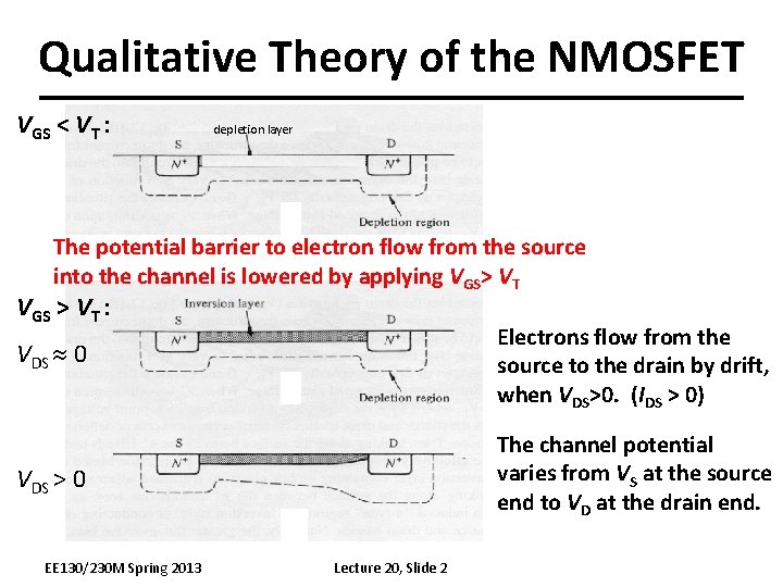
Qualitative Theory of the NMOSFET VGS < VT : depletion layer The potential barrier to electron flow from the source into the channel is lowered by applying VGS> VT VGS > VT : Electrons flow from the source to the drain by drift, when VDS>0. (IDS > 0) VDS 0 The channel potential varies from VS at the source end to VD at the drain end. VDS > 0 EE 130/230 M Spring 2013 Lecture 20, Slide 2
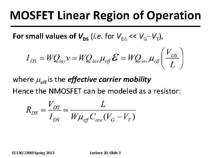
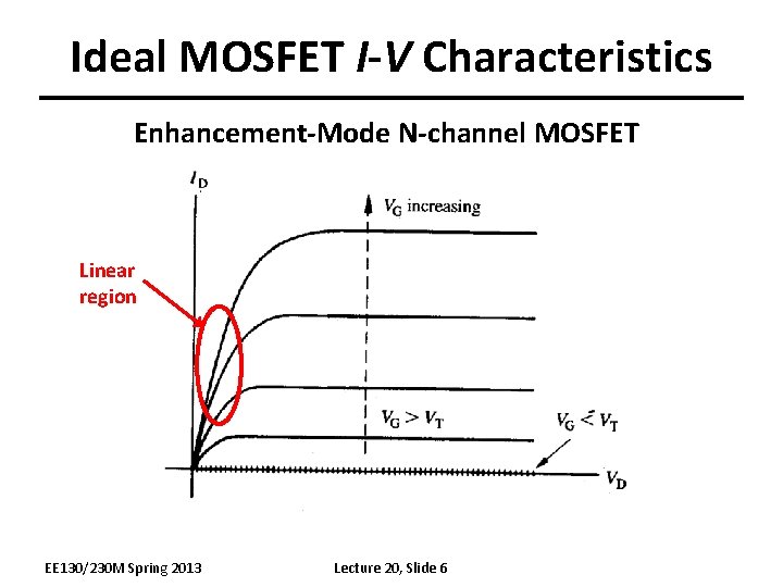
MOSFET Linear Region of Operation For small values of VDS (i. e. for VDS << VG VT), where meff is the effective carrier mobility Hence the NMOSFET can be modeled as a resistor: EE 130/230 M Spring 2013 Lecture 20, Slide 3
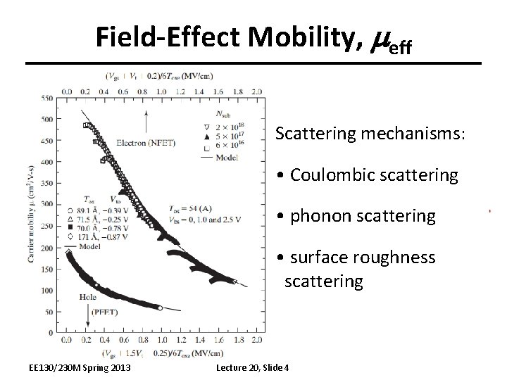
Field-Effect Mobility, meff Scattering mechanisms: • Coulombic scattering • phonon scattering • surface roughness scattering EE 130/230 M Spring 2013 Lecture 20, Slide 4
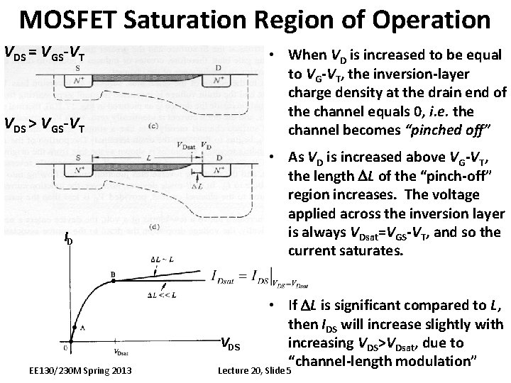
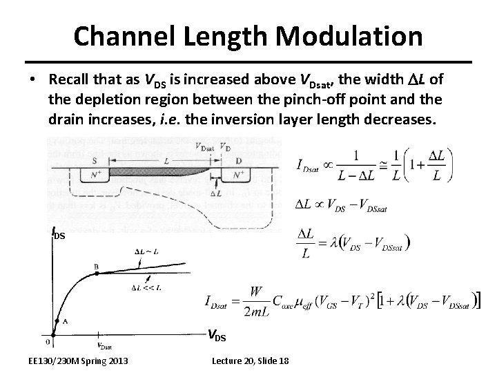
MOSFET Saturation Region of Operation VDS = VGS-VT VDS > VGS-VT ID EE 130/230 M Spring 2013 • When VD is increased to be equal to VG-VT, the inversion-layer charge density at the drain end of the channel equals 0, i. e. the channel becomes “pinched off” • As VD is increased above VG-VT, the length DL of the “pinch-off” region increases. The voltage applied across the inversion layer is always VDsat=VGS-VT, and so the current saturates. • If DL is significant compared to L, then IDS will increase slightly with VDS increasing VDS>VDsat, due to “channel-length modulation” Lecture 20, Slide 5
Ideal MOSFET I-V Characteristics Enhancement-Mode N-channel MOSFET Linear region EE 130/230 M Spring 2013 Lecture 20, Slide 6
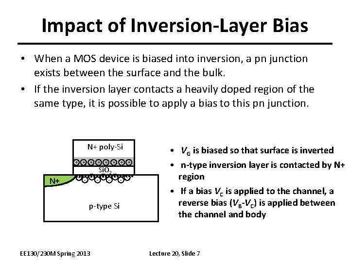
Impact of Inversion-Layer Bias • When a MOS device is biased into inversion, a pn junction exists between the surface and the bulk. • If the inversion layer contacts a heavily doped region of the same type, it is possible to apply a bias to this pn junction. N+ poly-Si + + + + Si. O 2 N+ - - - - - p-type Si EE 130/230 M Spring 2013 • VG is biased so that surface is inverted • n-type inversion layer is contacted by N+ region • If a bias VC is applied to the channel, a reverse bias (VB-VC) is applied between the channel and body Lecture 20, Slide 7
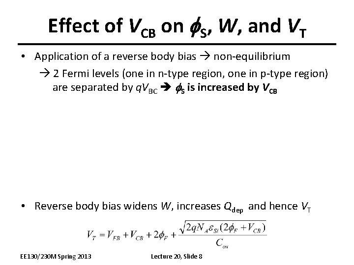
Effect of VCB on f. S, W, and VT • Application of a reverse body bias non-equilibrium 2 Fermi levels (one in n-type region, one in p-type region) are separated by q. VBC f. S is increased by VCB • Reverse body bias widens W, increases Qdep and hence VT EE 130/230 M Spring 2013 Lecture 20, Slide 8
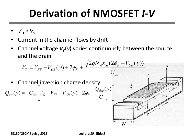
Derivation of NMOSFET I-V • VD > VS • Current in the channel flows by drift • Channel voltage VC(y) varies continuously between the source and the drain • Channel inversion charge density W EE 130/230 M Spring 2013 Lecture 20, Slide 9
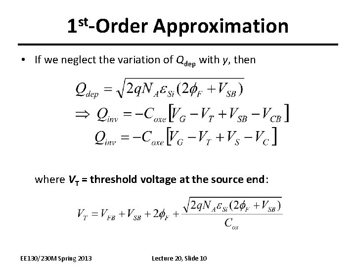
1 st-Order Approximation • If we neglect the variation of Qdep with y, then where VT = threshold voltage at the source end: EE 130/230 M Spring 2013 Lecture 20, Slide 10
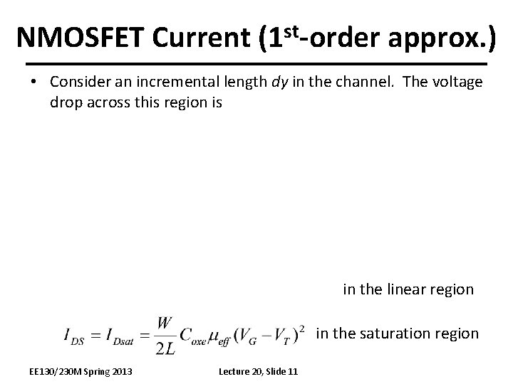
NMOSFET Current (1 st-order approx. ) • Consider an incremental length dy in the channel. The voltage drop across this region is in the linear region in the saturation region EE 130/230 M Spring 2013 Lecture 20, Slide 11
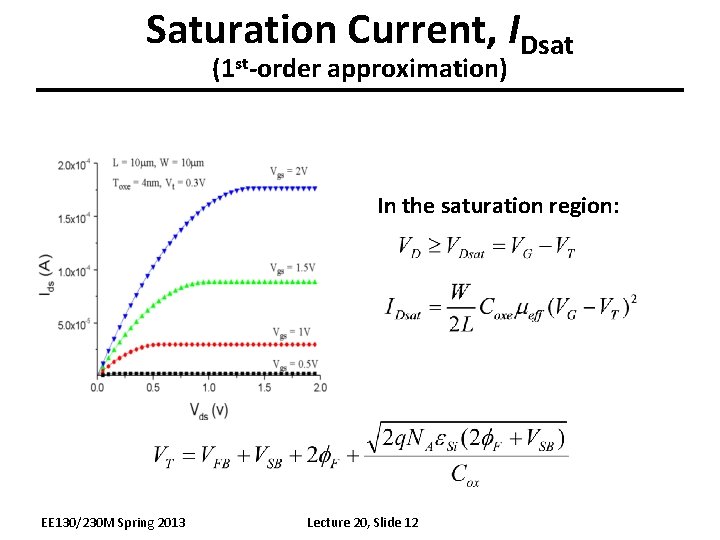
Saturation Current, IDsat (1 st-order approximation) In the saturation region: EE 130/230 M Spring 2013 Lecture 20, Slide 12
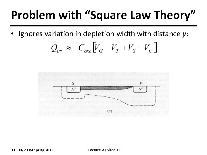
Problem with “Square Law Theory” • Ignores variation in depletion width with distance y: EE 130/230 M Spring 2013 Lecture 20, Slide 13
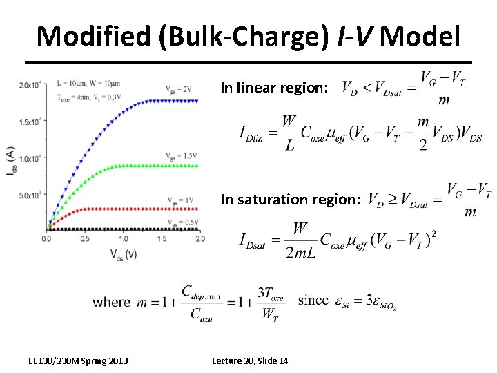
Modified (Bulk-Charge) I-V Model In linear region: In saturation region: EE 130/230 M Spring 2013 Lecture 20, Slide 14
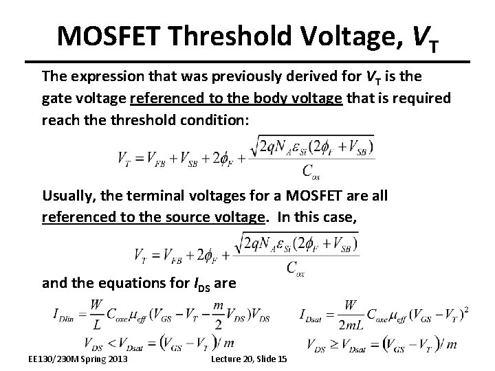
MOSFET Threshold Voltage, VT The expression that was previously derived for VT is the gate voltage referenced to the body voltage that is required reach the threshold condition: Usually, the terminal voltages for a MOSFET are all referenced to the source voltage. In this case, and the equations for IDS are EE 130/230 M Spring 2013 Lecture 20, Slide 15
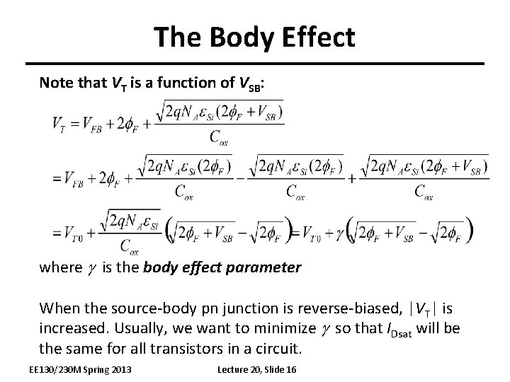
The Body Effect Note that VT is a function of VSB: where g is the body effect parameter When the source-body pn junction is reverse-biased, |VT| is increased. Usually, we want to minimize g so that IDsat will be the same for all transistors in a circuit. EE 130/230 M Spring 2013 Lecture 20, Slide 16
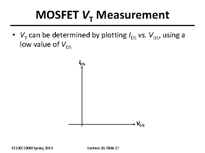
MOSFET VT Measurement • VT can be determined by plotting IDS vs. VGS, using a low value of VDS IDS VGS EE 130/230 M Spring 2013 Lecture 20, Slide 17
Channel Length Modulation • Recall that as VDS is increased above VDsat, the width DL of the depletion region between the pinch-off point and the drain increases, i. e. the inversion layer length decreases. IDS VDS EE 130/230 M Spring 2013 Lecture 20, Slide 18
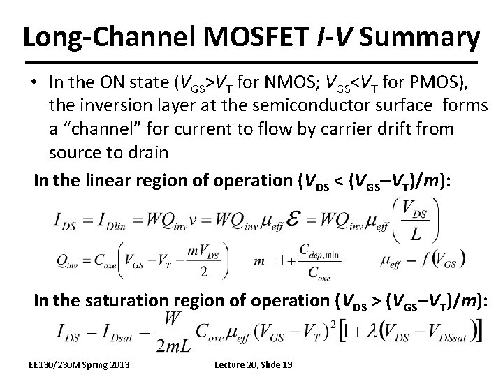
Long-Channel MOSFET I-V Summary • In the ON state (VGS>VT for NMOS; VGS<VT for PMOS), the inversion layer at the semiconductor surface forms a “channel” for current to flow by carrier drift from source to drain In the linear region of operation (VDS < (VGS VT)/m): In the saturation region of operation (VDS > (VGS VT)/m): EE 130/230 M Spring 2013 Lecture 20, Slide 19