Lecture 20 CAMs ROMs PLAs 20 CAMs ROMs

- Slides: 31

Lecture 20: CAMs, ROMs, PLAs 20: CAMs, ROMs, and PLAs 1

Outline q Content-Addressable Memories q Read-Only Memories q Programmable Logic Arrays 20: CAMs, ROMs, and PLAs CMOS VLSI Design 4 th Ed. 2

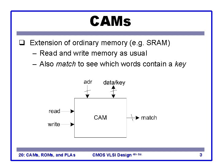
CAMs q Extension of ordinary memory (e. g. SRAM) – Read and write memory as usual – Also match to see which words contain a key 20: CAMs, ROMs, and PLAs CMOS VLSI Design 4 th Ed. 3

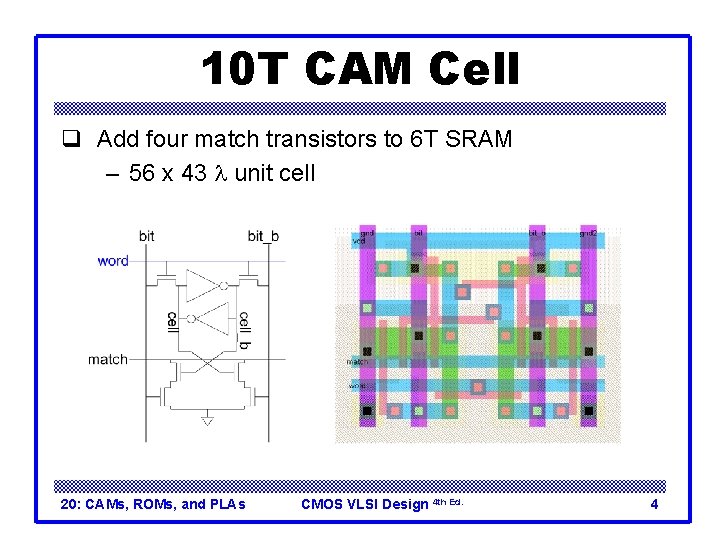
10 T CAM Cell q Add four match transistors to 6 T SRAM – 56 x 43 l unit cell 20: CAMs, ROMs, and PLAs CMOS VLSI Design 4 th Ed. 4

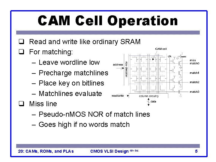
CAM Cell Operation q Read and write like ordinary SRAM q For matching: – Leave wordline low – Precharge matchlines – Place key on bitlines – Matchlines evaluate q Miss line – Pseudo-n. MOS NOR of match lines – Goes high if no words match 20: CAMs, ROMs, and PLAs CMOS VLSI Design 4 th Ed. 5

Read-Only Memories q Read-Only Memories are nonvolatile – Retain their contents when power is removed q Mask-programmed ROMs use one transistor per bit – Presence or absence determines 1 or 0 20: CAMs, ROMs, and PLAs CMOS VLSI Design 4 th Ed. 6

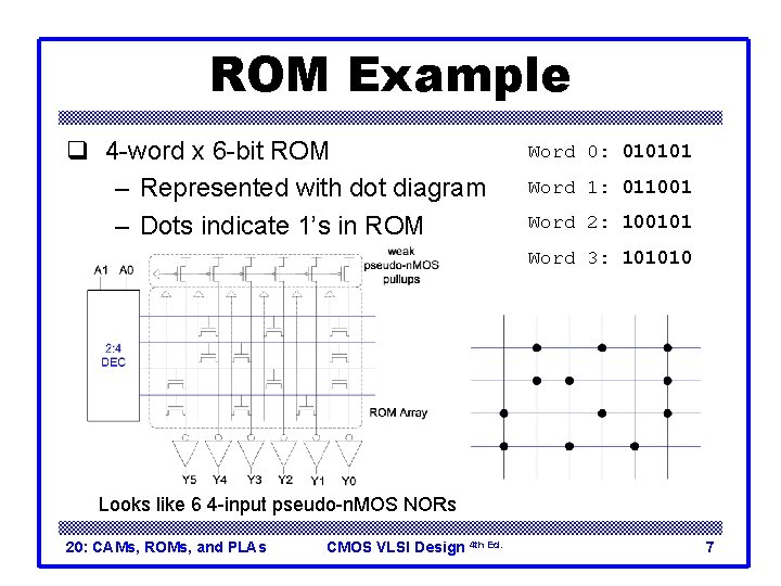
ROM Example q 4 -word x 6 -bit ROM – Represented with dot diagram – Dots indicate 1’s in ROM Word 0: 010101 Word 1: 011001 Word 2: 100101 Word 3: 101010 Looks like 6 4 -input pseudo-n. MOS NORs 20: CAMs, ROMs, and PLAs CMOS VLSI Design 4 th Ed. 7

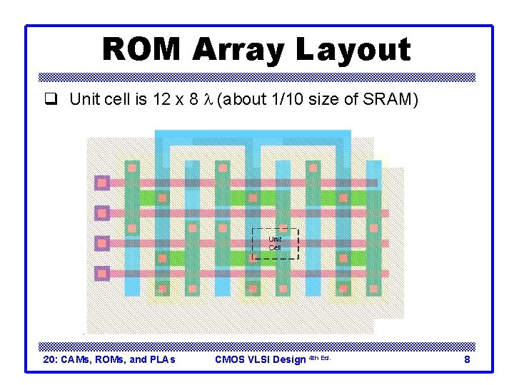
ROM Array Layout q Unit cell is 12 x 8 l (about 1/10 size of SRAM) 20: CAMs, ROMs, and PLAs CMOS VLSI Design 4 th Ed. 8

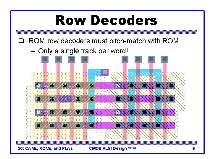
Row Decoders q ROM row decoders must pitch-match with ROM – Only a single track per word! 20: CAMs, ROMs, and PLAs CMOS VLSI Design 4 th Ed. 9

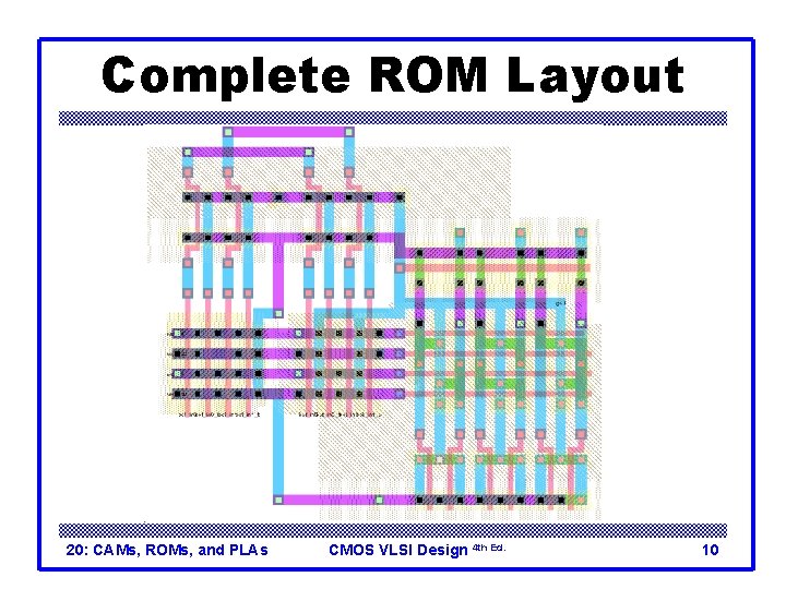
Complete ROM Layout 20: CAMs, ROMs, and PLAs CMOS VLSI Design 4 th Ed. 10

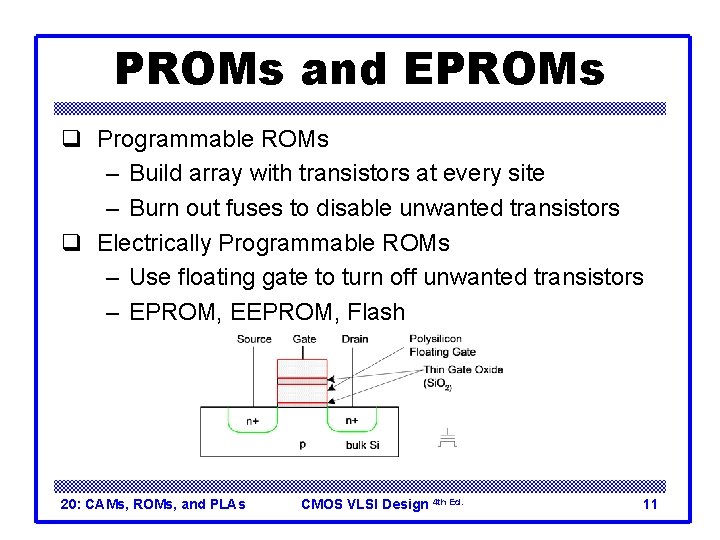
PROMs and EPROMs q Programmable ROMs – Build array with transistors at every site – Burn out fuses to disable unwanted transistors q Electrically Programmable ROMs – Use floating gate to turn off unwanted transistors – EPROM, EEPROM, Flash 20: CAMs, ROMs, and PLAs CMOS VLSI Design 4 th Ed. 11

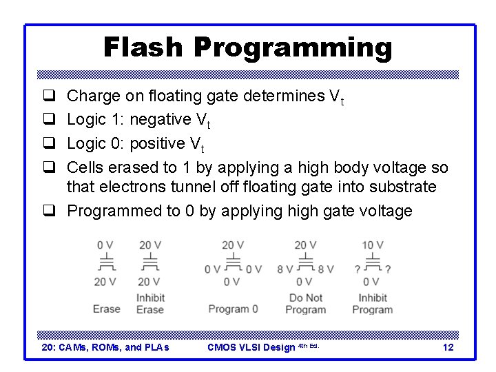
Flash Programming q q Charge on floating gate determines Vt Logic 1: negative Vt Logic 0: positive Vt Cells erased to 1 by applying a high body voltage so that electrons tunnel off floating gate into substrate q Programmed to 0 by applying high gate voltage 20: CAMs, ROMs, and PLAs CMOS VLSI Design 4 th Ed. 12

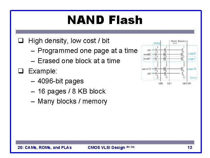
NAND Flash q High density, low cost / bit – Programmed one page at a time – Erased one block at a time q Example: – 4096 -bit pages – 16 pages / 8 KB block – Many blocks / memory 20: CAMs, ROMs, and PLAs CMOS VLSI Design 4 th Ed. 13

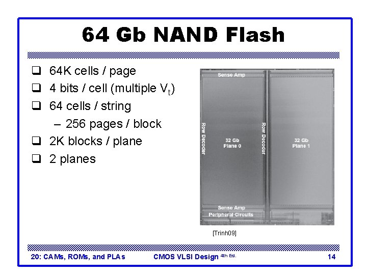
64 Gb NAND Flash q 64 K cells / page q 4 bits / cell (multiple Vt) q 64 cells / string – 256 pages / block q 2 K blocks / plane q 2 planes [Trinh 09] 20: CAMs, ROMs, and PLAs CMOS VLSI Design 4 th Ed. 14

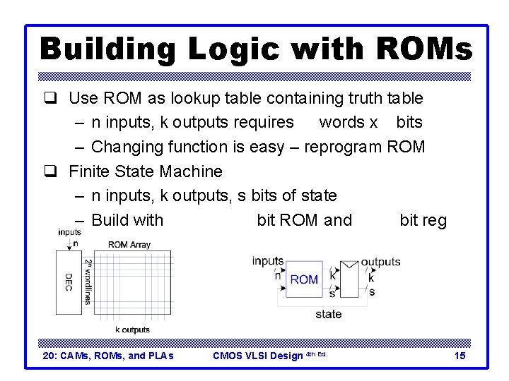
Building Logic with ROMs q Use ROM as lookup table containing truth table – n inputs, k outputs requires 2 n words x k bits – Changing function is easy – reprogram ROM q Finite State Machine – n inputs, k outputs, s bits of state – Build with 2 n+s x (k+s) bit ROM and (k+s) bit reg 20: CAMs, ROMs, and PLAs CMOS VLSI Design 4 th Ed. 15

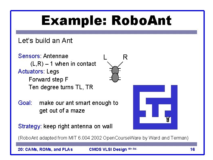
Example: Robo. Ant Let’s build an Ant Sensors: Antennae (L, R) – 1 when in contact Actuators: Legs Forward step F Ten degree turns TL, TR Goal: L R make our ant smart enough to get out of a maze Strategy: keep right antenna on wall (Robo. Ant adapted from MIT 6. 004 2002 Open. Course. Ware by Ward and Terman) 20: CAMs, ROMs, and PLAs CMOS VLSI Design 4 th Ed. 16

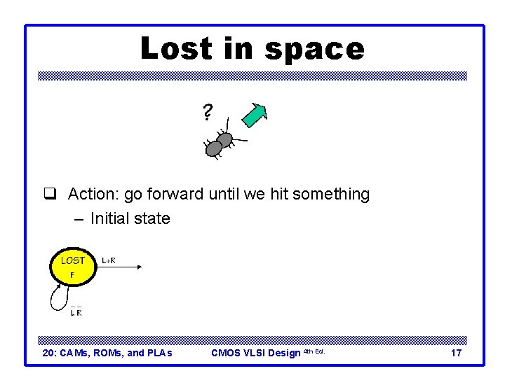
Lost in space q Action: go forward until we hit something – Initial state 20: CAMs, ROMs, and PLAs CMOS VLSI Design 4 th Ed. 17

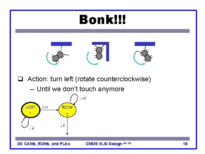
Bonk!!! q Action: turn left (rotate counterclockwise) – Until we don’t touch anymore 20: CAMs, ROMs, and PLAs CMOS VLSI Design 4 th Ed. 18

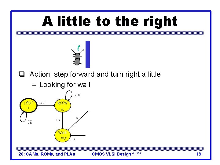
A little to the right q Action: step forward and turn right a little – Looking for wall 20: CAMs, ROMs, and PLAs CMOS VLSI Design 4 th Ed. 19

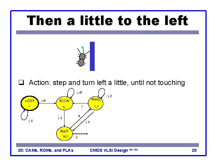
Then a little to the left q Action: step and turn left a little, until not touching 20: CAMs, ROMs, and PLAs CMOS VLSI Design 4 th Ed. 20

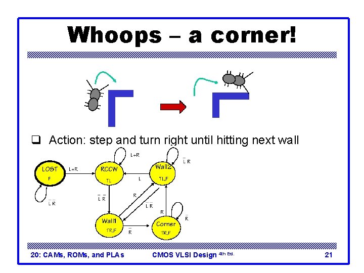
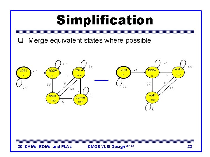
Whoops – a corner! q Action: step and turn right until hitting next wall 20: CAMs, ROMs, and PLAs CMOS VLSI Design 4 th Ed. 21

Simplification q Merge equivalent states where possible 20: CAMs, ROMs, and PLAs CMOS VLSI Design 4 th Ed. 22

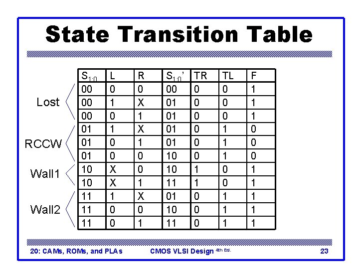
State Transition Table Lost RCCW Wall 1 Wall 2 S 1: 0 00 01 01 01 10 10 11 11 11 L 0 1 0 0 X X 1 0 0 20: CAMs, ROMs, and PLAs R 0 X 1 0 0 1 X 0 1 S 1: 0’ 00 01 01 10 10 11 01 10 11 TR 0 0 0 1 1 0 0 0 TL 0 0 0 1 1 1 CMOS VLSI Design 4 th Ed. F 1 1 1 0 0 0 1 1 1 23

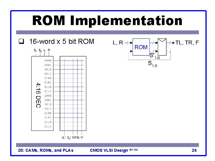
ROM Implementation q 16 -word x 5 bit ROM 20: CAMs, ROMs, and PLAs CMOS VLSI Design 4 th Ed. 24

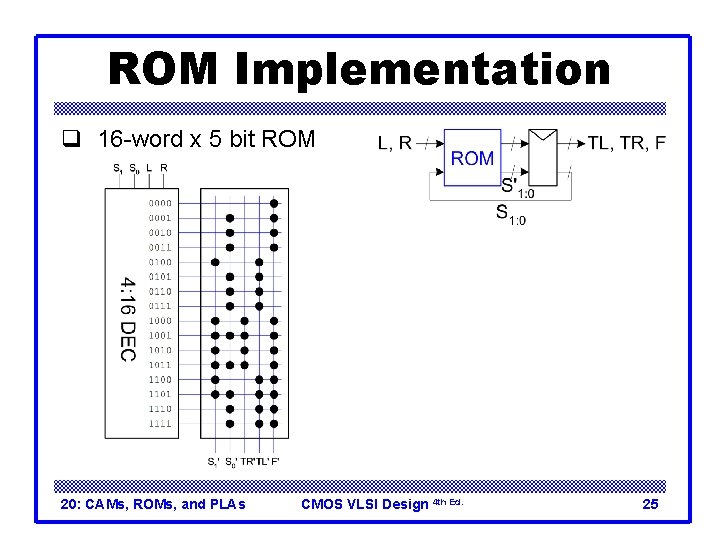
ROM Implementation q 16 -word x 5 bit ROM 20: CAMs, ROMs, and PLAs CMOS VLSI Design 4 th Ed. 25

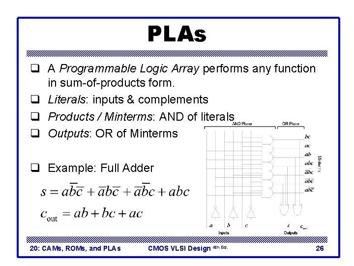
PLAs q A Programmable Logic Array performs any function in sum-of-products form. q Literals: inputs & complements q Products / Minterms: AND of literals q Outputs: OR of Minterms q Example: Full Adder 20: CAMs, ROMs, and PLAs CMOS VLSI Design 4 th Ed. 26

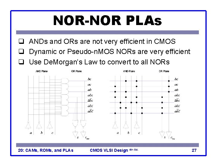
NOR-NOR PLAs q ANDs and ORs are not very efficient in CMOS q Dynamic or Pseudo-n. MOS NORs are very efficient q Use De. Morgan’s Law to convert to all NORs 20: CAMs, ROMs, and PLAs CMOS VLSI Design 4 th Ed. 27

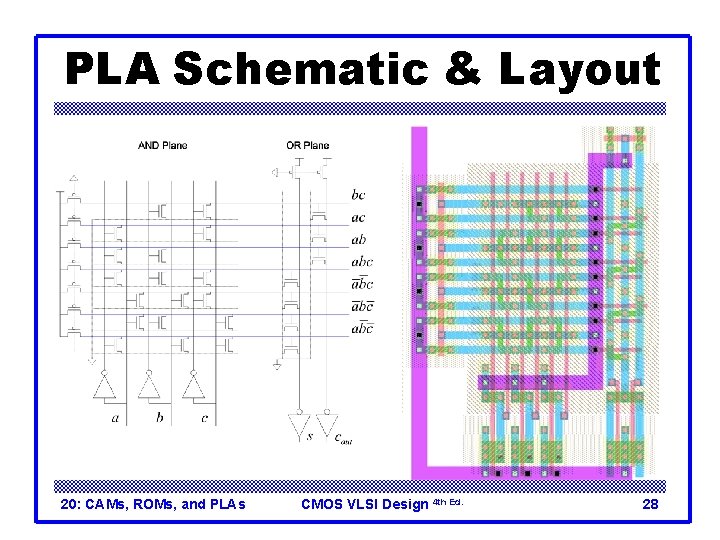
PLA Schematic & Layout 20: CAMs, ROMs, and PLAs CMOS VLSI Design 4 th Ed. 28

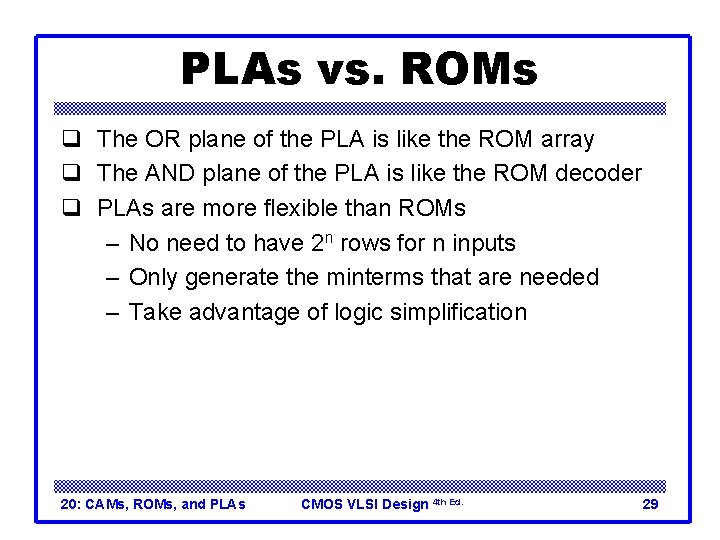
PLAs vs. ROMs q The OR plane of the PLA is like the ROM array q The AND plane of the PLA is like the ROM decoder q PLAs are more flexible than ROMs – No need to have 2 n rows for n inputs – Only generate the minterms that are needed – Take advantage of logic simplification 20: CAMs, ROMs, and PLAs CMOS VLSI Design 4 th Ed. 29

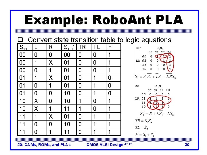
Example: Robo. Ant PLA q Convert state transition table to logic equations S 1: 0 00 01 01 01 10 10 11 11 11 L 0 1 0 0 X X 1 0 0 R 0 X 1 0 0 1 X 0 1 S 1: 0’ 00 01 01 10 10 11 01 10 11 20: CAMs, ROMs, and PLAs TR 0 0 0 1 1 0 0 0 TL 0 0 0 1 1 1 F 1 1 1 0 0 0 1 1 1 CMOS VLSI Design 4 th Ed. 30

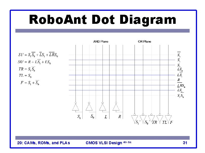
Robo. Ant Dot Diagram 20: CAMs, ROMs, and PLAs CMOS VLSI Design 4 th Ed. 31