Lecture 2 Wafer and Epitaxy Techniques Semiconductor Substrate

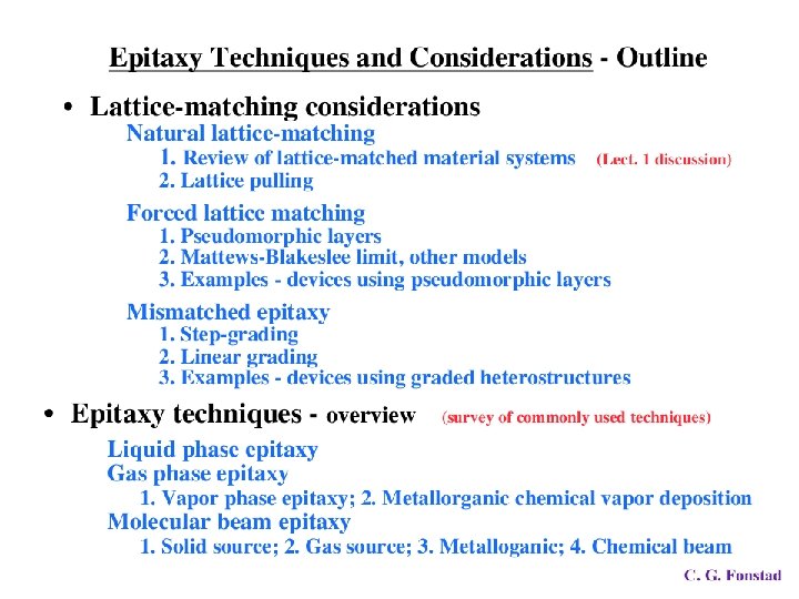
Lecture 2: Wafer and Epitaxy Techniques Semiconductor Substrate Production: Si, Ga. As, In. P, Ga. P, In. As, In. Sb……. Si. C, Sapphire, Ga. N Wafer Growth: (1)Czochralski Growth (CZ) (2)Bridgman Growth of Ga. As (3)Float Zone Growth see Campbell Book pp. 10 -33 for (2)(3)
")
Czochralski Growth (CZ)


200 mm Si wafer CZ facility 300 mm Si wafer in manufacture

Ga. As CZ Schematic Picture LEC =Liquid Encapsulated Czochralski growth Ga. As melts at 1238 C. The vapor of Ga is less than 0. 001 atm, while the vapor prssure of arsenic is about 10000 larger.

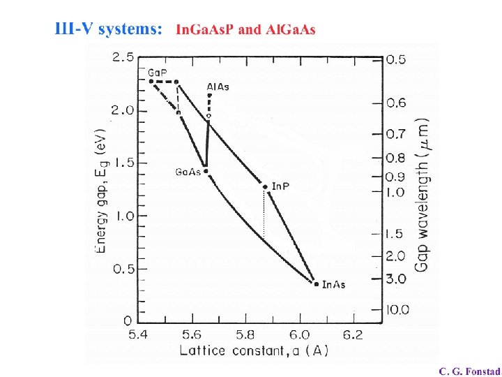
Ga. As MESFET commercial products made directly from Ga. As substrate In. P MOSFET (made in Purdue) directly fabricated from In. P substrate (by Yanqing Wu) Better quality ? Epitaxy

Still Active Research Field, e. g. , APL High-mobility two-dimensional electron gas in In. Al. As/In. As heterostructures grown on virtual In. As substrates by molecular-beam epitaxy Y. Lin, J. A. Carlin, A. R. Arehart, A. M. Carlin, and S. A. Ringel Department of Electrical and Computer Engineering, The Ohio State University, Columbus, Ohio 43210 (Received 6 July 2006; accepted 4 December 2006; published online 5 January 2007)

Experts at Purdue Prof. Woodall Prof. Melloch
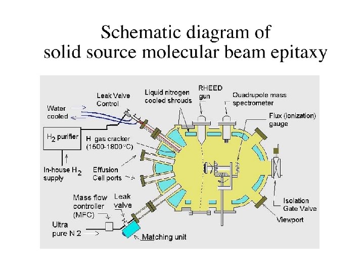
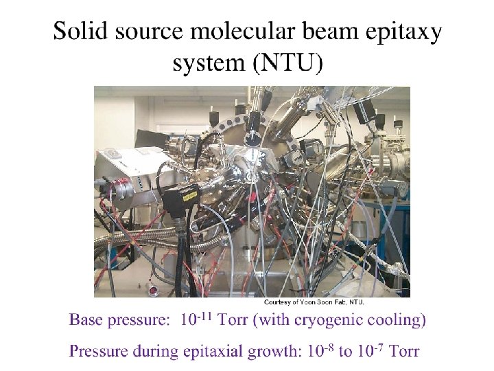
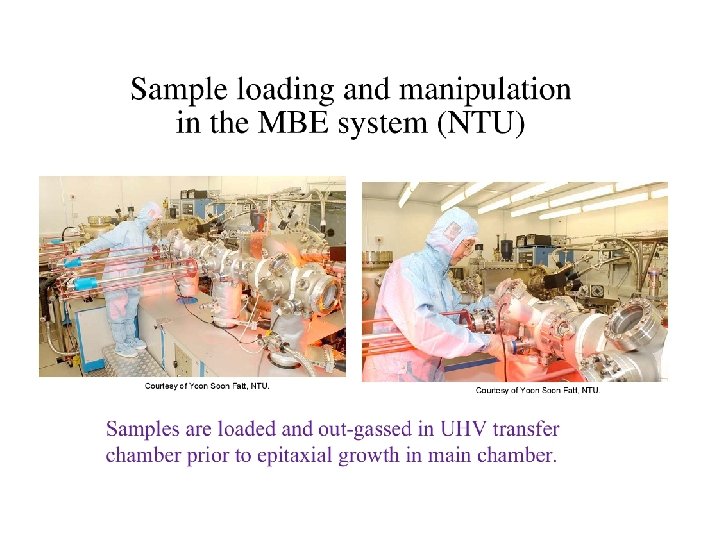
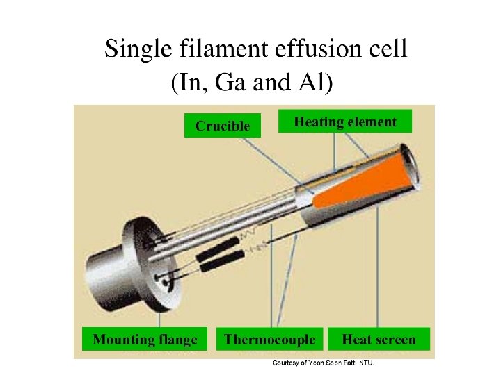
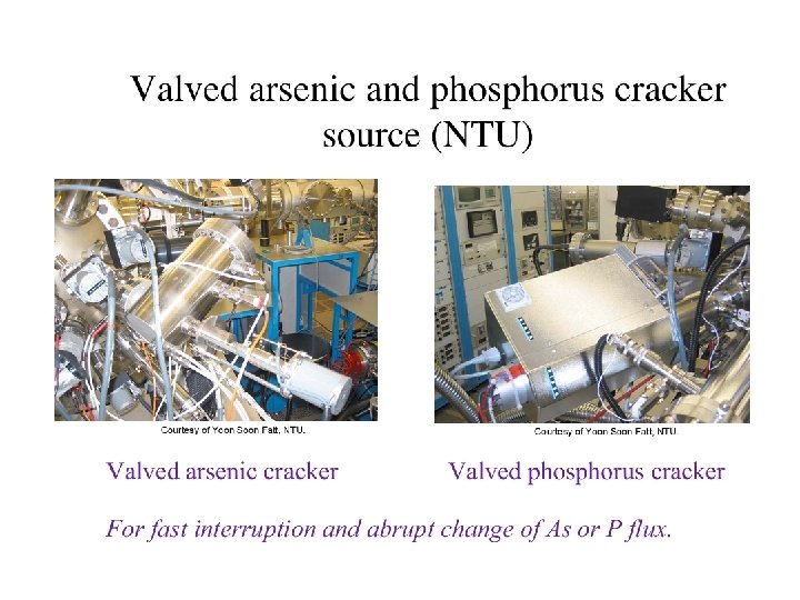
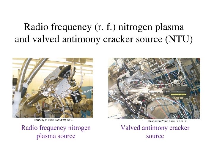
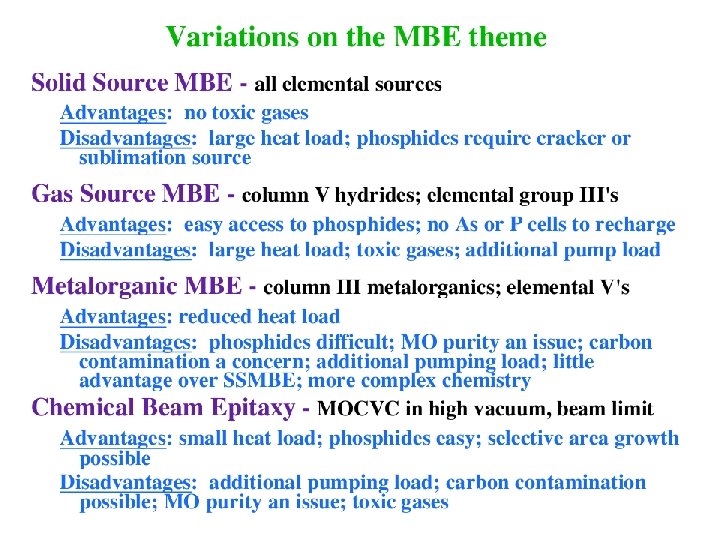
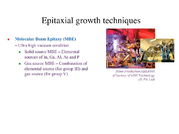

Homework: Read Campbell Book: 1. Chapter 2 pp. 10 -33 2. Chapter 14. 11, 14. 13 pp. 378 -391 Please write 2 paragraph and also use 1 Figure from website or lecture notes to describe what MBE is. Due time next Thursday.
- Slides: 22