Lecture 2 Operational Amplifiers 1 Goals Understand behavior
Lecture 2 Operational Amplifiers 1
Goals • Understand behavior and characteristics of ideal op amps. • Demonstrate circuit analysis techniques for ideal op amps. • Characterize inverting, non-inverting, summing and difference amplifiers, voltage follower and integrator. • Learns factors involved in circuit design using op amps. 2
Ideal Operation Amplifier (Op Amp) Ideal op amps are assumed to have infinite voltage gain, and infinite input resistance. These conditions lead to two assumptions useful in analyzing ideal op amp circuits: 1. The voltage difference across the input terminals is zero. 2. The input currents are zero.
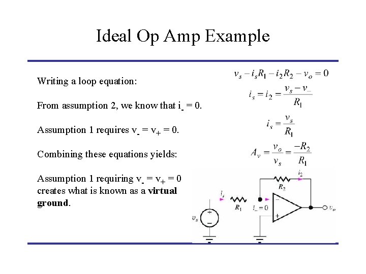
Ideal Op Amp Example Writing a loop equation: From assumption 2, we know that i- = 0. Assumption 1 requires v- = v+ = 0. Combining these equations yields: Assumption 1 requiring v- = v+ = 0 creates what is known as a virtual ground.
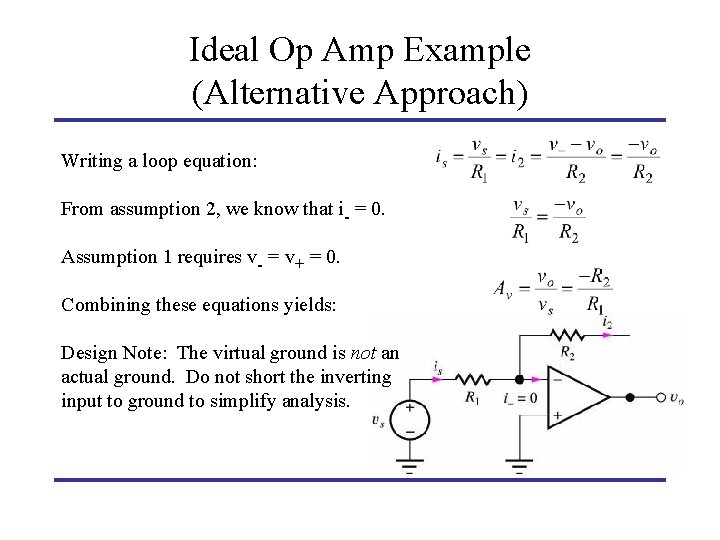
Ideal Op Amp Example (Alternative Approach) Writing a loop equation: From assumption 2, we know that i- = 0. Assumption 1 requires v- = v+ = 0. Combining these equations yields: Design Note: The virtual ground is not an actual ground. Do not short the inverting input to ground to simplify analysis.
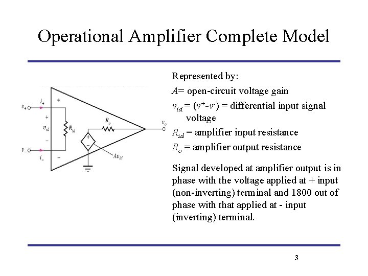
Operational Amplifier Complete Model Represented by: A= open-circuit voltage gain vid = (v+-v-) = differential input signal voltage Rid = amplifier input resistance Ro = amplifier output resistance Signal developed at amplifier output is in phase with the voltage applied at + input (non-inverting) terminal and 1800 out of phase with that applied at - input (inverting) terminal. 3
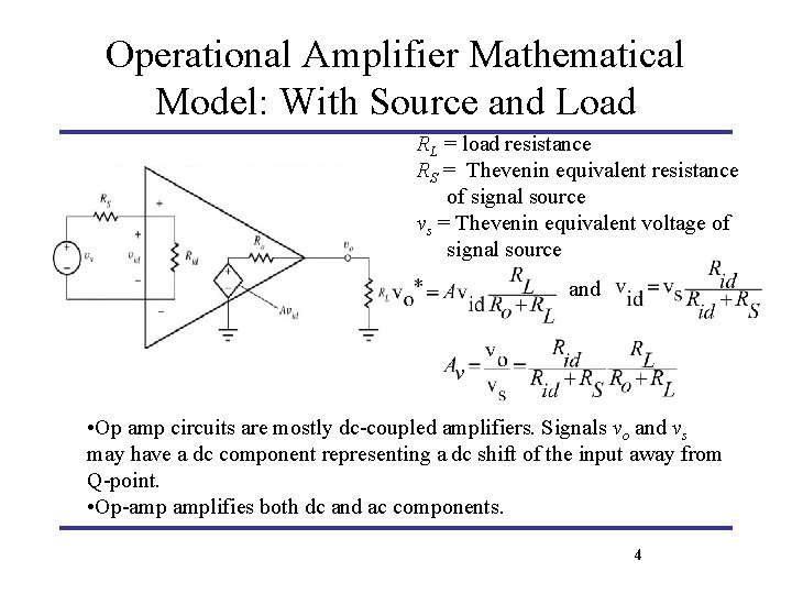
Operational Amplifier Mathematical Model: With Source and Load RL = load resistance RS = Thevenin equivalent resistance of signal source vs = Thevenin equivalent voltage of signal source and • Op amp circuits are mostly dc-coupled amplifiers. Signals vo and vs may have a dc component representing a dc shift of the input away from Q-point. • Op-amp amplifies both dc and ac components. 4
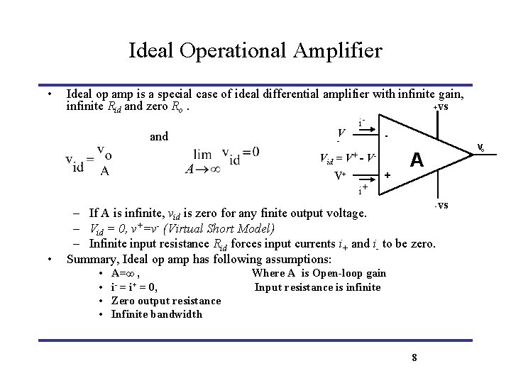
Ideal Operational Amplifier • Ideal op amp is a special case of ideal differential amplifier with infinite gain, +VS infinite Rid and zero Ro. and V i- - - Vid = V+ V+ - V+ Vo A i+ -VS • – If A is infinite, vid is zero for any finite output voltage. – Vid = 0, v+=v- (Virtual Short Model) – Infinite input resistance Rid forces input currents i+ and i- to be zero. Summary, Ideal op amp has following assumptions: • • A=∞ , i- = i+ = 0, Zero output resistance Infinite bandwidth Where A is Open-loop gain Input resistance is infinite 8
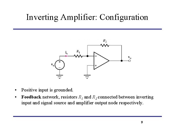
Inverting Amplifier: Configuration • Positive input is grounded. • Feedback network, resistors R 1 and R 2 connected between inverting input and signal source and amplifier output node respectively. 9
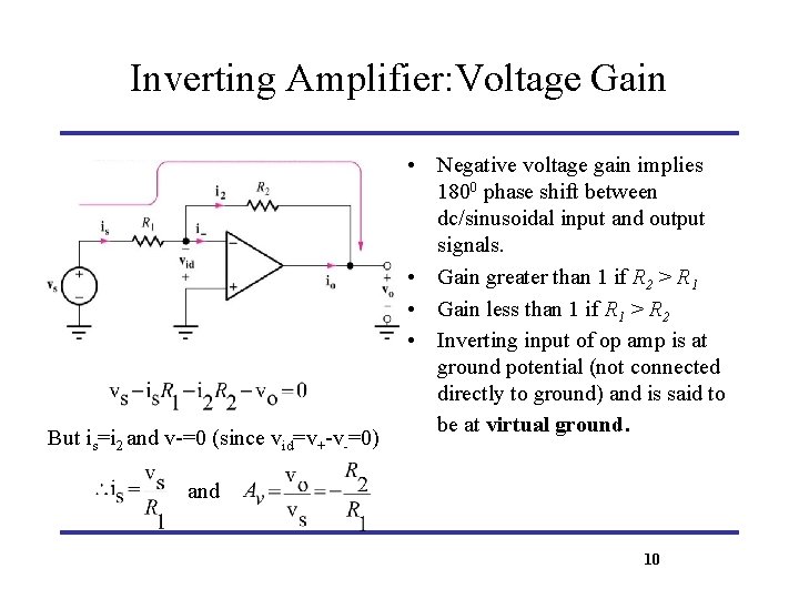
Inverting Amplifier: Voltage Gain But is=i 2 and v-=0 (since vid=v+-v-=0) • Negative voltage gain implies 1800 phase shift between dc/sinusoidal input and output signals. • Gain greater than 1 if R 2 > R 1 • Gain less than 1 if R 1 > R 2 • Inverting input of op amp is at ground potential (not connected directly to ground) and is said to be at virtual ground. and 10
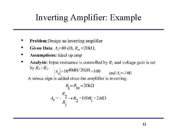
Inverting Amplifier: Example 11
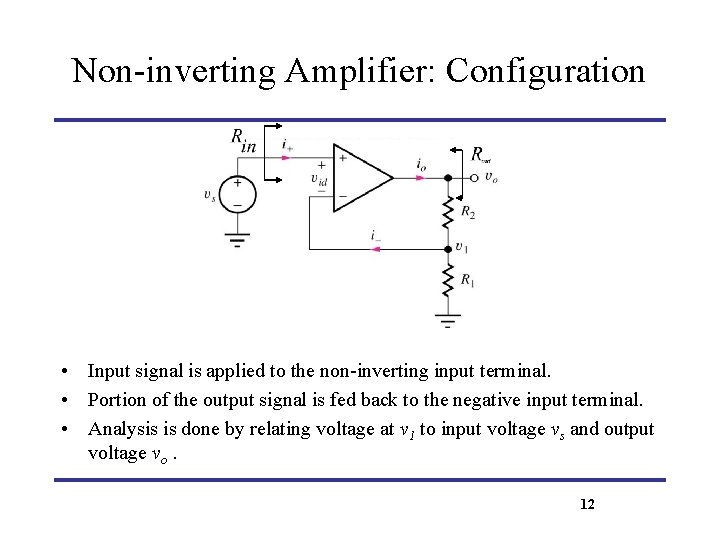
Non-inverting Amplifier: Configuration • Input signal is applied to the non-inverting input terminal. • Portion of the output signal is fed back to the negative input terminal. • Analysis is done by relating voltage at v 1 to input voltage vs and output voltage vo. 12
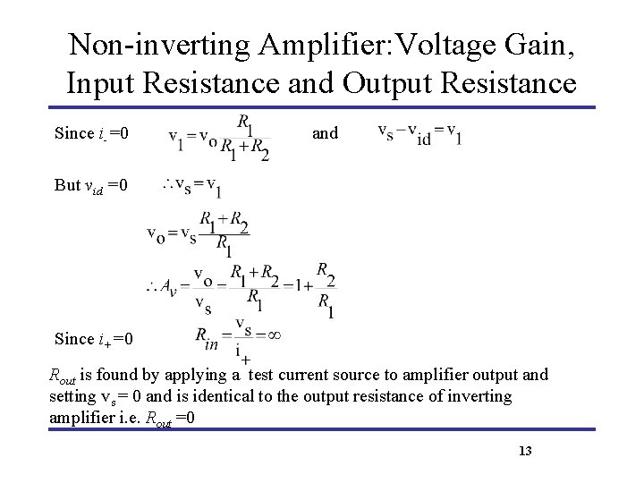
Non-inverting Amplifier: Voltage Gain, Input Resistance and Output Resistance Since i-=0 and But vid =0 Since i+=0 Rout is found by applying a test current source to amplifier output and setting vs = 0 and is identical to the output resistance of inverting amplifier i. e. Rout =0 13
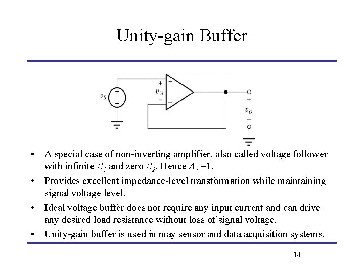
Unity-gain Buffer • A special case of non-inverting amplifier, also called voltage follower with infinite R 1 and zero R 2. Hence Av =1. • Provides excellent impedance-level transformation while maintaining signal voltage level. • Ideal voltage buffer does not require any input current and can drive any desired load resistance without loss of signal voltage. • Unity-gain buffer is used in may sensor and data acquisition systems. 14
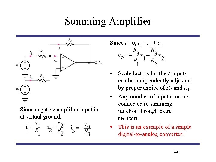
Summing Amplifier Since i-=0, i 3= i 1 + i 2, Since negative amplifier input is at virtual ground, • Scale factors for the 2 inputs can be independently adjusted by proper choice of R 2 and R 1. • Any number of inputs can be connected to summing junction through extra resistors. • This is an example of a simple digital-to-analog converter. 15
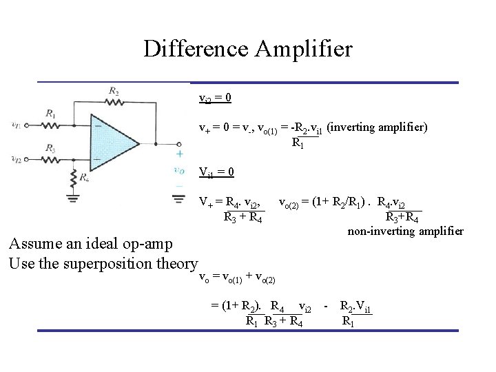
Difference Amplifier vi 2 = 0 v+ = 0 = v-, vo(1) = -R 2. vi 1 (inverting amplifier) R 1 Vi 1 = 0 V+ = R 4. vi 2, R 3 + R 4 Assume an ideal op-amp Use the superposition theory vo(2) = (1+ R 2/R 1). R 4. vi 2 R 3+R 4 non-inverting amplifier vo = vo(1) + vo(2) = (1+ R 2). R 4 vi 2 R 1 R 3 + R 4 - R 2. Vi 1 R 1
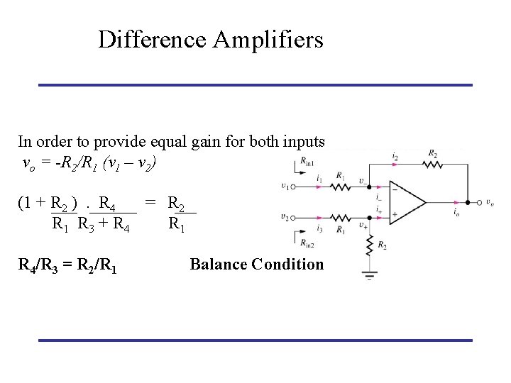
Difference Amplifiers In order to provide equal gain for both inputs vo = -R 2/R 1 (v 1 – v 2) (1 + R 2 ). R 4 = R 2 R 1 R 3 + R 4 R 1 R 4/R 3 = R 2/R 1 Balance Condition
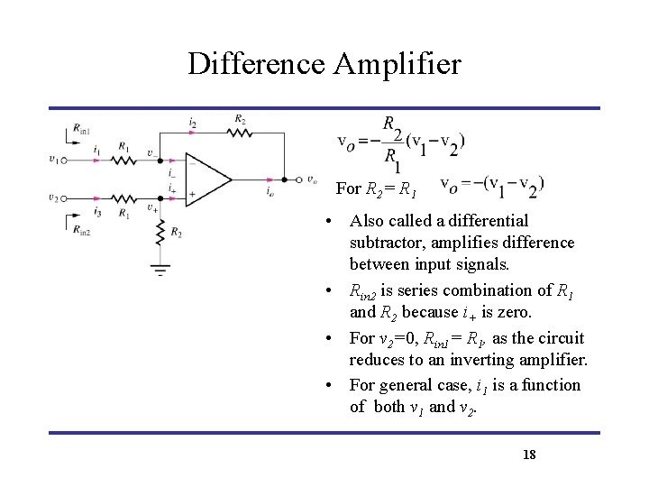
Difference Amplifier For R 2= R 1 • Also called a differential subtractor, amplifies difference between input signals. • Rin 2 is series combination of R 1 and R 2 because i+ is zero. • For v 2=0, Rin 1= R 1, as the circuit reduces to an inverting amplifier. • For general case, i 1 is a function of both v 1 and v 2. 18
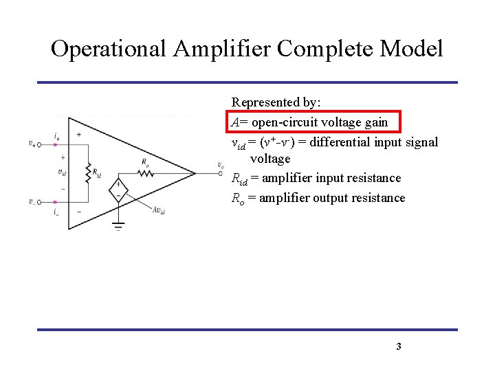
Operational Amplifier Complete Model Represented by: A= open-circuit voltage gain vid = (v+-v-) = differential input signal voltage Rid = amplifier input resistance Ro = amplifier output resistance 3
Non-ideal Operational Amplifier • Various error terms arise in practical operational amplifiers due to nonideal behavior. • Some of the non-ideal characteristics include: – √ Finite open-loop gain that causes gain error – Nonzero output resistance – Finite input resistance – Finite CMRR – Common-mode input resistance – √ DC error sources – √ Output voltage and current limits 20
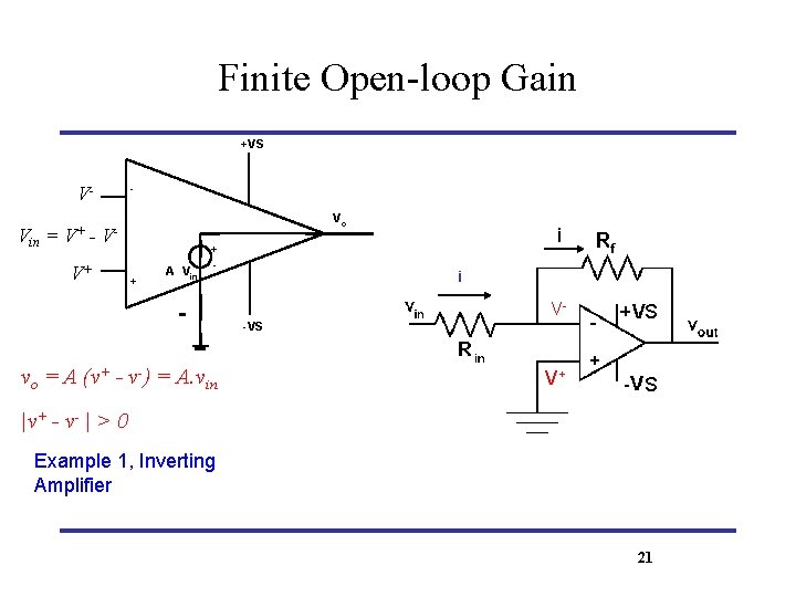
Finite Open-loop Gain +VS - VVin = V+ - Vo V- V+ + A Vin + - i i V- S V+ S -VS vo = A (v+ - v-) = A. vin |v+ - v- | > 0 Example 1, Inverting Amplifier 21
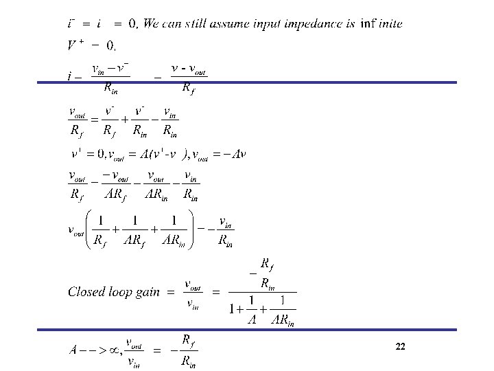
22
- Slides: 22