Lecture 2 Hardware Modeling with Verilog HDL 1



![Implicit Structural Model Example module bit_or (y, a, b); input [7: 0] a, b; Implicit Structural Model Example module bit_or (y, a, b); input [7: 0] a, b;](https://slidetodoc.com/presentation_image_h2/813bf92a4cfe70bd943e78d43286c936/image-12.jpg)
![Module Port Connections module parent_mod; wire [3: 0] g; child_mod G 1 (g[3], g[1], Module Port Connections module parent_mod; wire [3: 0] g; child_mod G 1 (g[3], g[1],](https://slidetodoc.com/presentation_image_h2/813bf92a4cfe70bd943e78d43286c936/image-13.jpg)
![Arrays of Instances module array_of_nor (y, a, b); input [7: 0] a, b; output Arrays of Instances module array_of_nor (y, a, b); input [7: 0] a, b; output](https://slidetodoc.com/presentation_image_h2/813bf92a4cfe70bd943e78d43286c936/image-21.jpg)
- Slides: 24

Lecture 2: Hardware Modeling with Verilog HDL 1

Verilog HDL: Hardware Modeling • Hardware Encapsulation: Verilog Module – Module Ports – Module Implementation • • Hardware Modeling: Verilog Primitives Descriptive Styles – Explicit Structural Description – Implicit Structural Description – Continuous Assignments • • • Structural Connections Behavioral Descriptions in Verilog Hierarchical Descriptions of Hardware Structural (Top-Down) Design Methodology Arrays of Instances Using Verilog for Synthesis 2

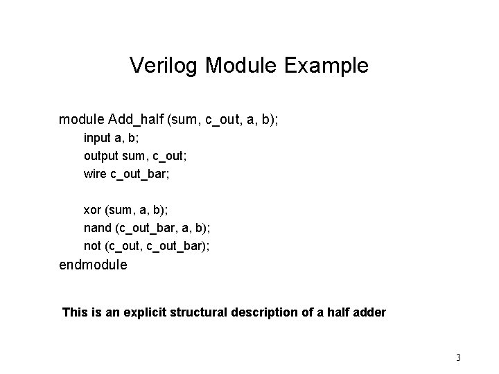
Verilog Module Example module Add_half (sum, c_out, a, b); input a, b; output sum, c_out; wire c_out_bar; xor (sum, a, b); nand (c_out_bar, a, b); not (c_out, c_out_bar); endmodule This is an explicit structural description of a half adder 3

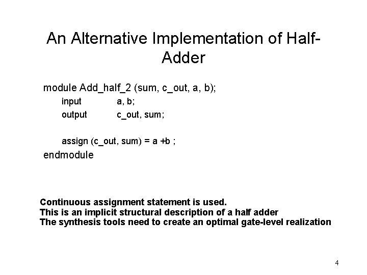
An Alternative Implementation of Half. Adder module Add_half_2 (sum, c_out, a, b); input output a, b; c_out, sum; assign (c_out, sum) = a +b ; endmodule Continuous assignment statement is used. This is an implicit structural description of a half adder The synthesis tools need to create an optimal gate-level realization 4

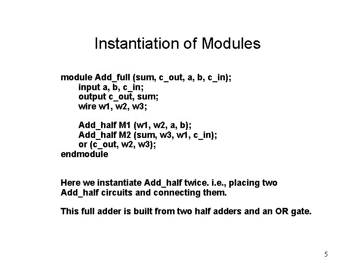
Instantiation of Modules module Add_full (sum, c_out, a, b, c_in); input a, b, c_in; output c_out, sum; wire w 1, w 2, w 3; Add_half M 1 (w 1, w 2, a, b); Add_half M 2 (sum, w 3, w 1, c_in); or (c_out, w 2, w 3); endmodule Here we instantiate Add_half twice. i. e. , placing two Add_half circuits and connecting them. This full adder is built from two half adders and an OR gate. 5

Verilog Primitives • Verilog primitives implement pre-defined hardware-based behavior. – Built-in primitives – User-Defined Primitives (UDP) • • All pre-defined primitives are combinational. The output of a combinational primitive must be of type “net”. The inputs of a primitive can be of type “net” or “reg” Verilog supports combinational and sequential UDP. 6

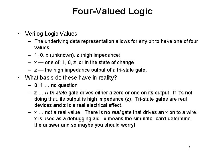
Four-Valued Logic • Verilog Logic Values – The underlying data representation allows for any bit to have one of four values – 1, 0, x (unknown), z (high impedance) – x — one of: 1, 0, z, or in the state of change – z — the high impedance output of a tri-state gate. • What basis do these have in reality? – 0, 1 … no question – z … A tri-state gate drives either a zero or one on its output. If it’s not doing that, its output is high impedance (z). Tri-state gates are real devices and z is a real electrical affect. – x … not a real value. There is no real gate that drives an x on to a wire. x is used as a debugging aid. x means the simulator can’t determine the answer and so maybe you should worry! 7

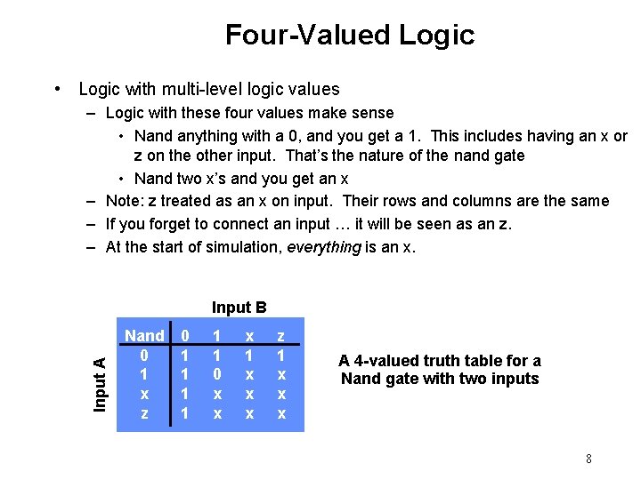
Four-Valued Logic • Logic with multi-level logic values – Logic with these four values make sense • Nand anything with a 0, and you get a 1. This includes having an x or z on the other input. That’s the nature of the nand gate • Nand two x’s and you get an x – Note: z treated as an x on input. Their rows and columns are the same – If you forget to connect an input … it will be seen as an z. – At the start of simulation, everything is an x. Input A Input B Nand 0 1 x z 0 1 1 1 0 x x x 1 x x x z 1 x x x A 4 -valued truth table for a Nand gate with two inputs 8

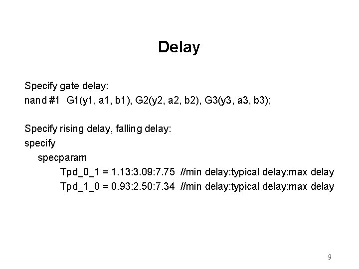
Delay Specify gate delay: nand #1 G 1(y 1, a 1, b 1), G 2(y 2, a 2, b 2), G 3(y 3, a 3, b 3); Specify rising delay, falling delay: specify specparam Tpd_0_1 = 1. 13: 3. 09: 7. 75 //min delay: typical delay: max delay Tpd_1_0 = 0. 93: 2. 50: 7. 34 //min delay: typical delay: max delay 9

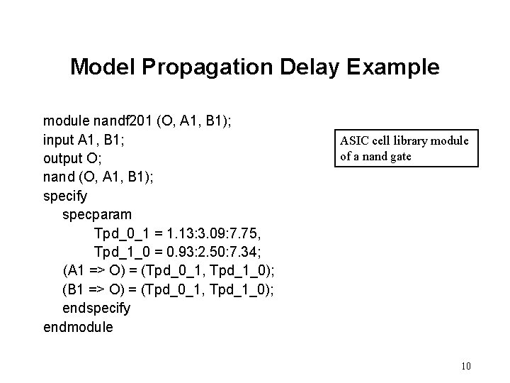
Model Propagation Delay Example module nandf 201 (O, A 1, B 1); input A 1, B 1; output O; nand (O, A 1, B 1); specify specparam Tpd_0_1 = 1. 13: 3. 09: 7. 75, Tpd_1_0 = 0. 93: 2. 50: 7. 34; (A 1 => O) = (Tpd_0_1, Tpd_1_0); (B 1 => O) = (Tpd_0_1, Tpd_1_0); endspecify endmodule ASIC cell library module of a nand gate 10

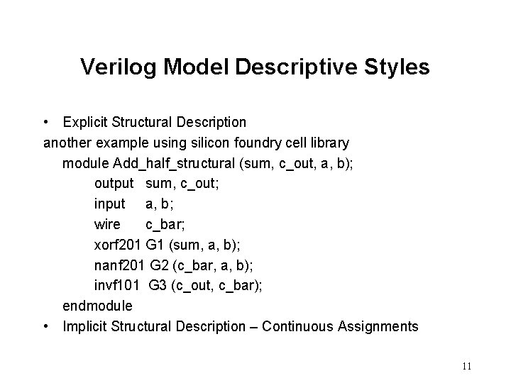
Verilog Model Descriptive Styles • Explicit Structural Description another example using silicon foundry cell library module Add_half_structural (sum, c_out, a, b); output sum, c_out; input a, b; wire c_bar; xorf 201 G 1 (sum, a, b); nanf 201 G 2 (c_bar, a, b); invf 101 G 3 (c_out, c_bar); endmodule • Implicit Structural Description – Continuous Assignments 11
![Implicit Structural Model Example module bitor y a b input 7 0 a b Implicit Structural Model Example module bit_or (y, a, b); input [7: 0] a, b;](https://slidetodoc.com/presentation_image_h2/813bf92a4cfe70bd943e78d43286c936/image-12.jpg)
Implicit Structural Model Example module bit_or (y, a, b); input [7: 0] a, b; // declare a, b 8 -bit wide output [7: 0] y; assign y = a I b; //bitwise or endmodule // another example module adder (sum, a, b); parameter width = 7; input [width: 0] a, b; output [width: 0] sum; assign sum = a + b; endmodule 12
![Module Port Connections module parentmod wire 3 0 g childmod G 1 g3 g1 Module Port Connections module parent_mod; wire [3: 0] g; child_mod G 1 (g[3], g[1],](https://slidetodoc.com/presentation_image_h2/813bf92a4cfe70bd943e78d43286c936/image-13.jpg)
Module Port Connections module parent_mod; wire [3: 0] g; child_mod G 1 (g[3], g[1], g[0], g[2]); // listed order is significant endmodule child_mod (sig_a, sig_b, sig_c, sig_d); input sig_a, sig_b; output sig_c, sig_d; // child_mod design is here endmodule 13

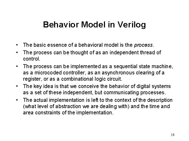
Behavior Model in Verilog • The basic essence of a behavioral model is the process. • The process can be thought of as an independent thread of control. • The process can be implemented as a sequential state machine, as a microcoded controller, as an asynchronous clearing of a register, or as a combinational logic circuit. • The key idea is that we conceive the behavior of digital systems as a set of these independent, but communicating processes. • The actual implementation is left to the context of the description (what level of abstraction we are dealing with) and the time and area constraints of the implementation. 14

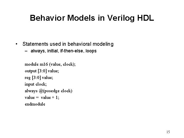
Behavior Models in Verilog HDL • Statements used in behavioral modeling – always, initial, if-then-else, loops module m 16 (value, clock); output [3: 0] value; reg [3: 0] value; input clock; always @(posedge clock) value = value + 1; endmodule 15

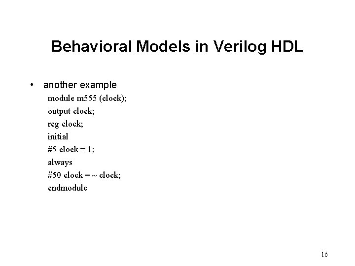
Behavioral Models in Verilog HDL • another example module m 555 (clock); output clock; reg clock; initial #5 clock = 1; always #50 clock = ~ clock; endmodule 16

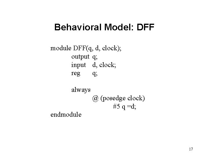
Behavioral Model: DFF module DFF(q, d, clock); output q; input d, clock; reg q; always @ (posedge clock) #5 q =d; endmodule 17

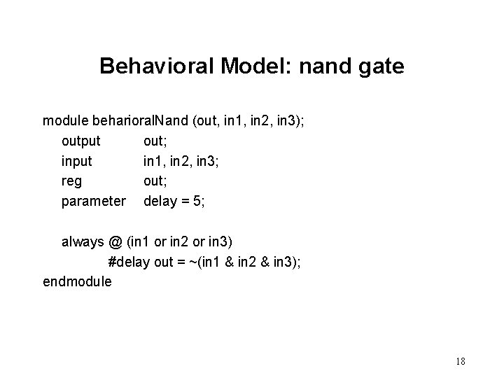
Behavioral Model: nand gate module beharioral. Nand (out, in 1, in 2, in 3); output out; input in 1, in 2, in 3; reg out; parameter delay = 5; always @ (in 1 or in 2 or in 3) #delay out = ~(in 1 & in 2 & in 3); endmodule 18

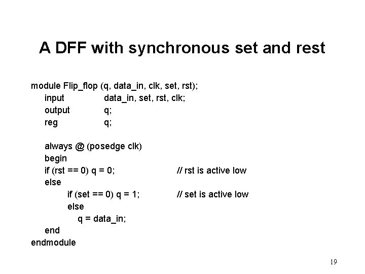
A DFF with synchronous set and rest module Flip_flop (q, data_in, clk, set, rst); input data_in, set, rst, clk; output q; reg q; always @ (posedge clk) begin if (rst == 0) q = 0; else if (set == 0) q = 1; else q = data_in; endmodule // rst is active low // set is active low 19

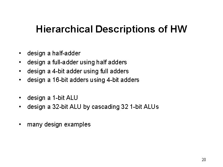
Hierarchical Descriptions of HW • • design a half-adder design a full-adder using half adders design a 4 -bit adder using full adders design a 16 -bit adders using 4 -bit adders • design a 1 -bit ALU • design a 32 -bit ALU by cascading 32 1 -bit ALUs • many design examples 20
![Arrays of Instances module arrayofnor y a b input 7 0 a b output Arrays of Instances module array_of_nor (y, a, b); input [7: 0] a, b; output](https://slidetodoc.com/presentation_image_h2/813bf92a4cfe70bd943e78d43286c936/image-21.jpg)
Arrays of Instances module array_of_nor (y, a, b); input [7: 0] a, b; output [7: 0] y; nor [7: 0] (y, a, b); endmodule array_of_flops (q, data_in, clk, set, rst); input [7: 0] data_in; input clk, set, rst; output [7: 0] q; Flip_flop M[7: 0] (q, data_in, clk, set, rst); endmodule 21

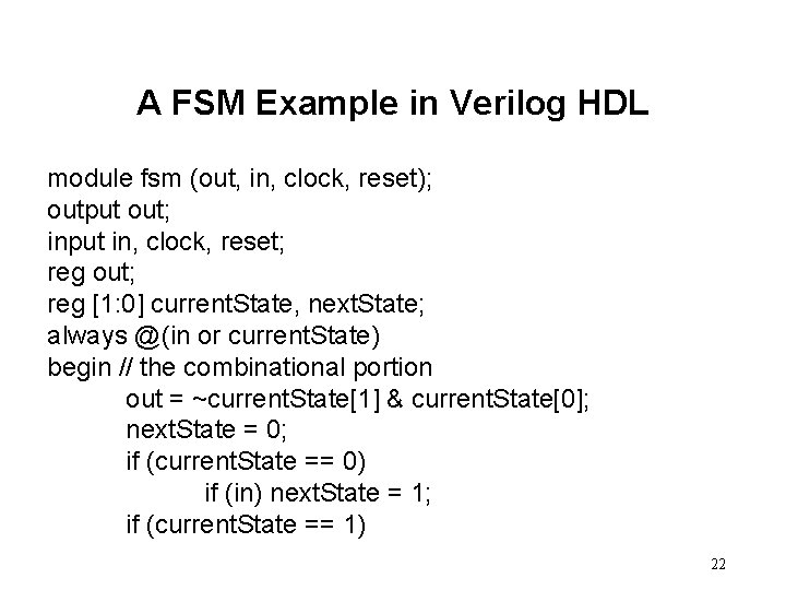
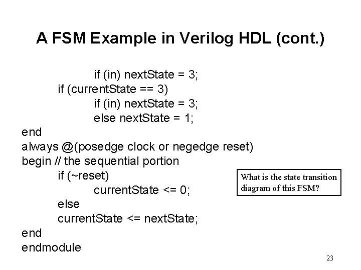
A FSM Example in Verilog HDL module fsm (out, in, clock, reset); output out; input in, clock, reset; reg out; reg [1: 0] current. State, next. State; always @(in or current. State) begin // the combinational portion out = ~current. State[1] & current. State[0]; next. State = 0; if (current. State == 0) if (in) next. State = 1; if (current. State == 1) 22

A FSM Example in Verilog HDL (cont. ) if (in) next. State = 3; if (current. State == 3) if (in) next. State = 3; else next. State = 1; end always @(posedge clock or negedge reset) begin // the sequential portion if (~reset) What is the state transition diagram of this FSM? current. State <= 0; else current. State <= next. State; endmodule 23

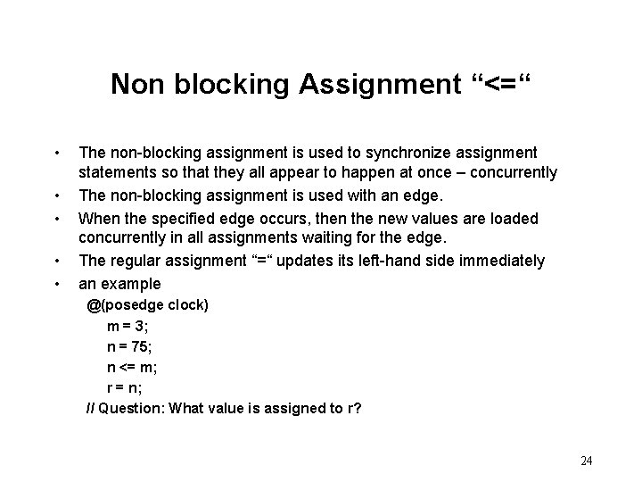
Non blocking Assignment “<=“ • • • The non-blocking assignment is used to synchronize assignment statements so that they all appear to happen at once – concurrently The non-blocking assignment is used with an edge. When the specified edge occurs, then the new values are loaded concurrently in all assignments waiting for the edge. The regular assignment “=“ updates its left-hand side immediately an example @(posedge clock) m = 3; n = 75; n <= m; r = n; // Question: What value is assigned to r? 24