Lecture 16 OUTLINE The MOS Capacitor contd Electrostatics
- Slides: 16

Lecture 16 OUTLINE • The MOS Capacitor (cont’d) – Electrostatics Reading: Pierret 16. 3; Hu 5. 2 -5. 5

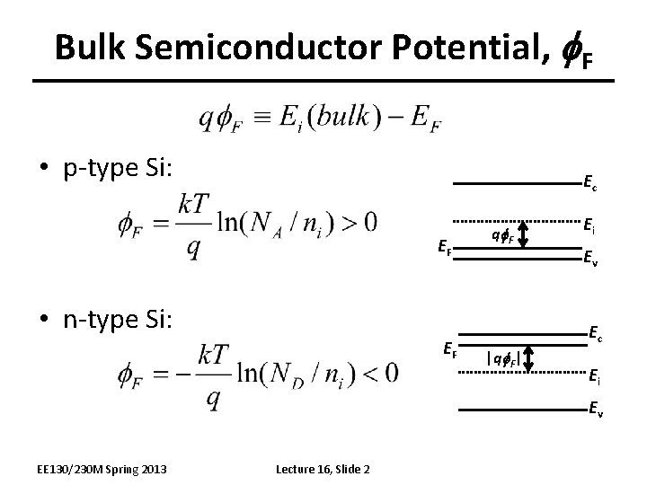
Bulk Semiconductor Potential, f. F • p-type Si: Ec EF qf. F • n-type Si: EF Ei Ev Ec |qf. F| Ei Ev EE 130/230 M Spring 2013 Lecture 16, Slide 2

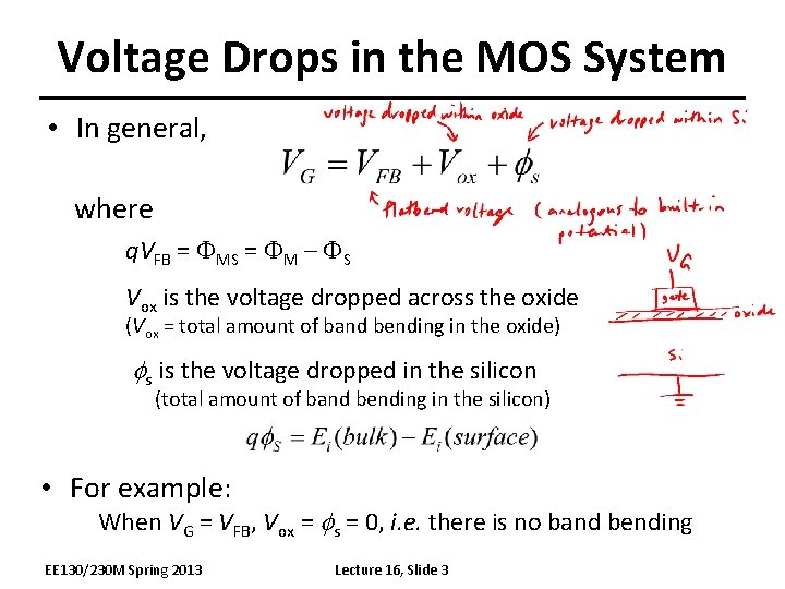
Voltage Drops in the MOS System • In general, where q. VFB = FMS = FM – FS Vox is the voltage dropped across the oxide (Vox = total amount of band bending in the oxide) fs is the voltage dropped in the silicon (total amount of band bending in the silicon) • For example: When VG = VFB, Vox = fs = 0, i. e. there is no band bending EE 130/230 M Spring 2013 Lecture 16, Slide 3

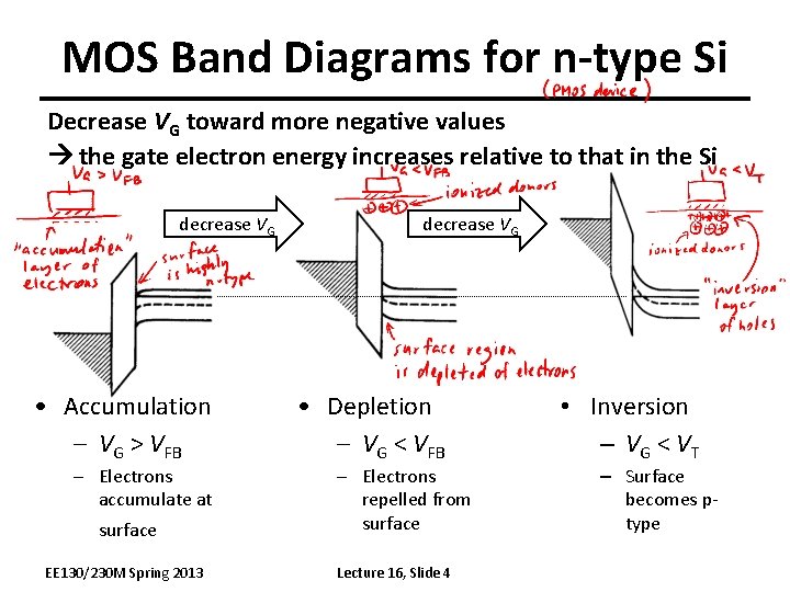
MOS Band Diagrams for n-type Si Decrease VG toward more negative values the gate electron energy increases relative to that in the Si decrease VG • Accumulation – VG > VFB – Electrons accumulate at surface EE 130/230 M Spring 2013 decrease VG • Depletion – VG < VFB – Electrons repelled from surface Lecture 16, Slide 4 • Inversion – VG < VT – Surface becomes ptype

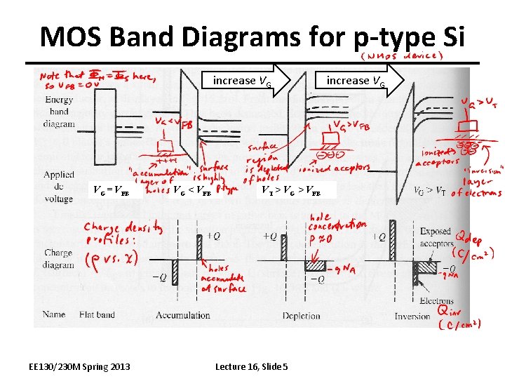
MOS Band Diagrams for p-type Si increase VG VG = VFB EE 130/230 M Spring 2013 VG < VFB VT > VG > VFB Lecture 16, Slide 5 increase VG

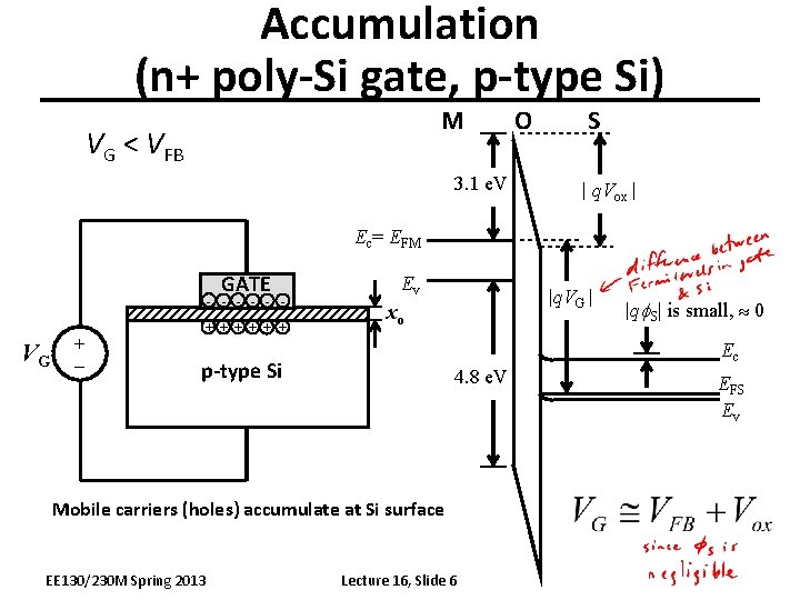
Accumulation (n+ poly-Si gate, p-type Si) M VG < VFB 3. 1 e. V O S | q. Vox | Ec= EFM GATE - - - VG + _ + + + Ev |q. VG | xo Ec p-type Si 4. 8 e. V Mobile carriers (holes) accumulate at Si surface EE 130/230 M Spring 2013 |qf. S| is small, 0 Lecture 16, Slide 6 EFS Ev

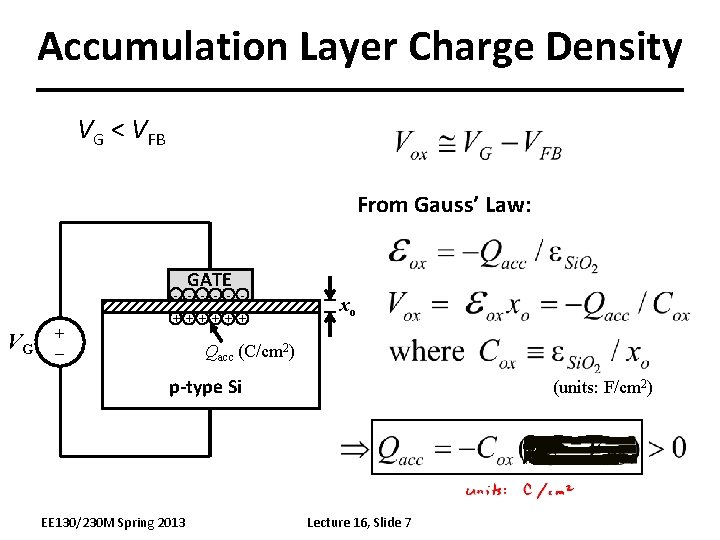
Accumulation Layer Charge Density VG < VFB From Gauss’ Law: GATE - - - VG + _ + + + xo Qacc (C/cm 2) p-type Si EE 130/230 M Spring 2013 (units: F/cm 2) Lecture 16, Slide 7

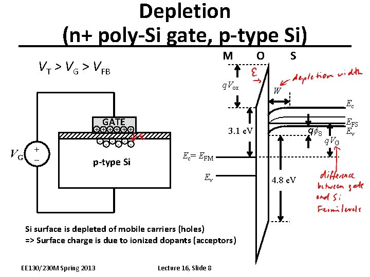
Depletion (n+ poly-Si gate, p-type Si) M VT > VG > VFB q. Vox O S W Ec GATE VG + _ qf S 3. 1 e. V + + + - - - p-type Si Ec= EFM Ev Si surface is depleted of mobile carriers (holes) => Surface charge is due to ionized dopants (acceptors) EE 130/230 M Spring 2013 Lecture 16, Slide 8 4. 8 e. V q. VG EFS Ev

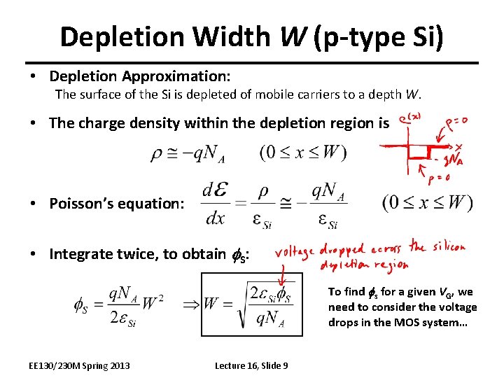
Depletion Width W (p-type Si) • Depletion Approximation: The surface of the Si is depleted of mobile carriers to a depth W. • The charge density within the depletion region is • Poisson’s equation: • Integrate twice, to obtain f. S: To find fs for a given VG, we need to consider the voltage drops in the MOS system… EE 130/230 M Spring 2013 Lecture 16, Slide 9

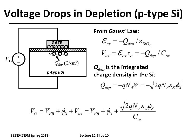
Voltage Drops in Depletion (p-type Si) From Gauss’ Law: GATE + + + VG - - - + _ Qdep (C/cm 2) p-type Si EE 130/230 M Spring 2013 Qdep is the integrated charge density in the Si: Lecture 16, Slide 10

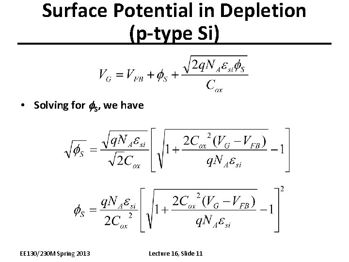
Surface Potential in Depletion (p-type Si) • Solving for f. S, we have EE 130/230 M Spring 2013 Lecture 16, Slide 11

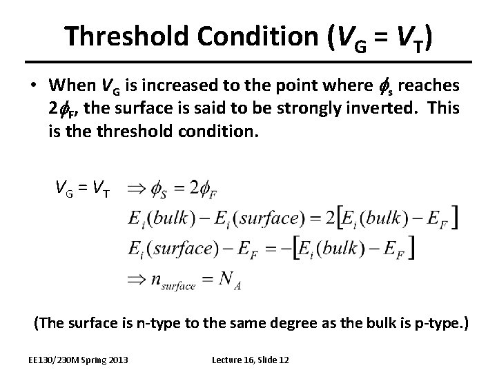
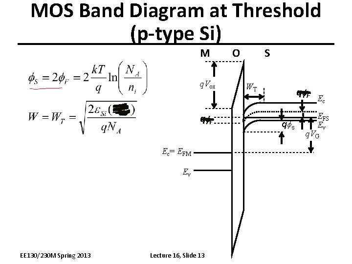
Threshold Condition (VG = VT) • When VG is increased to the point where fs reaches 2 f. F, the surface is said to be strongly inverted. This is the threshold condition. VG = VT (The surface is n-type to the same degree as the bulk is p-type. ) EE 130/230 M Spring 2013 Lecture 16, Slide 12

MOS Band Diagram at Threshold (p-type Si) M q. Vox qf. F Ec= EFM Ev EE 130/230 M Spring 2013 Lecture 16, Slide 13 O S WT qf. F qf s Ec EFS Ev q. VG

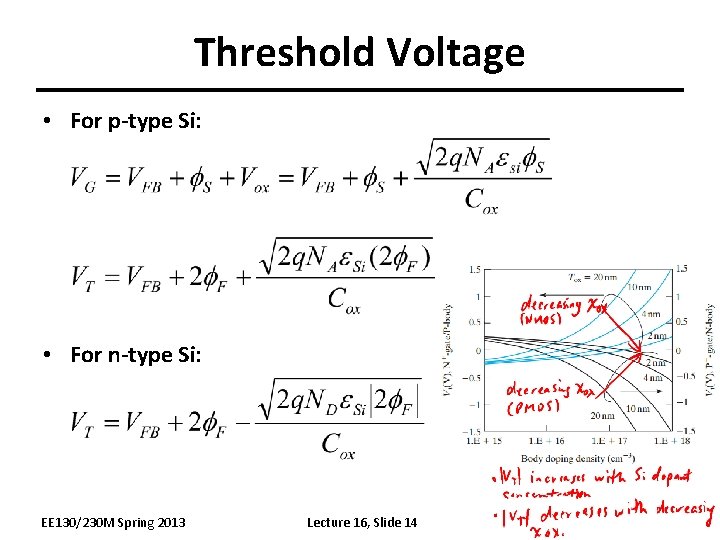
Threshold Voltage • For p-type Si: • For n-type Si: EE 130/230 M Spring 2013 Lecture 16, Slide 14

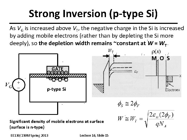
Strong Inversion (p-type Si) As VG is increased above VT, the negative charge in the Si is increased by adding mobile electrons (rather than by depleting the Si more deeply), so the depletion width remains ~constant at W = WT WT r(x) M O S GATE + + + VG + _ x - - - p-type Si Significant density of mobile electrons at surface (surface is n-type) EE 130/230 M Spring 2013 Lecture 16, Slide 15

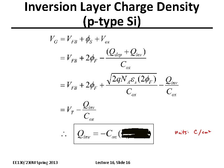
Inversion Layer Charge Density (p-type Si) EE 130/230 M Spring 2013 Lecture 16, Slide 16