
Lecture 16 OUTLINE Diode analysis and applications continued
- Slides: 29
Lecture #16 OUTLINE • Diode analysis and applications continued • The MOSFET – The MOSFET as a controlled resistor – Pinch-off and current saturation – Channel-length modulation – Velocity saturation in a short-channel MOSFET Reading • Rabaey et al. – Chapter 3. 3. 1 -3. 3. 2 • Hambley – Chapter 12. 1 EECS 40, Fall 2004 Lecture 16, Slide 1 Prof. White
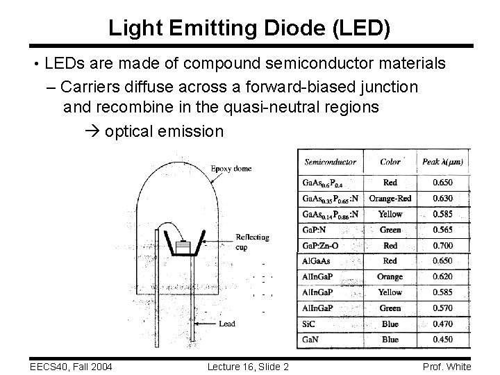
Light Emitting Diode (LED) • LEDs are made of compound semiconductor materials – Carriers diffuse across a forward-biased junction and recombine in the quasi-neutral regions optical emission EECS 40, Fall 2004 Lecture 16, Slide 2 Prof. White
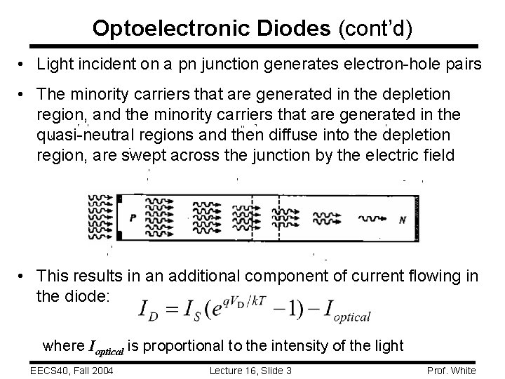
Optoelectronic Diodes (cont’d) • Light incident on a pn junction generates electron-hole pairs • The minority carriers that are generated in the depletion region, and the minority carriers that are generated in the quasi-neutral regions and then diffuse into the depletion region, are swept across the junction by the electric field • This results in an additional component of current flowing in the diode: where Ioptical is proportional to the intensity of the light EECS 40, Fall 2004 Lecture 16, Slide 3 Prof. White
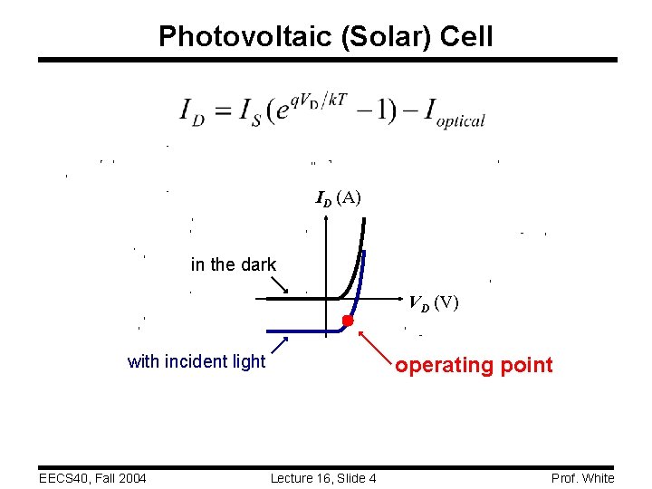
Photovoltaic (Solar) Cell ID (A) in the dark VD (V) with incident light EECS 40, Fall 2004 operating point Lecture 16, Slide 4 Prof. White
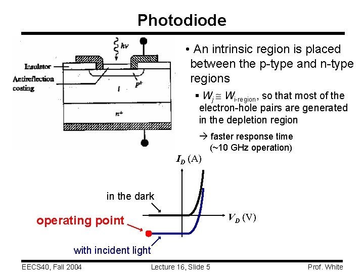
Photodiode • An intrinsic region is placed between the p-type and n-type regions § Wj Wi-region, so that most of the electron-hole pairs are generated in the depletion region faster response time (~10 GHz operation) ID (A) in the dark VD (V) operating point with incident light EECS 40, Fall 2004 Lecture 16, Slide 5 Prof. White
Why are pn Junctions Important for ICs? • The basic building block in digital ICs is the MOS transistor, whose structure contains reverse-biased diodes. – pn junctions are important for electrical isolation of transistors located next to each other at the surface of a Si wafer. – The junction capacitance of these diodes can limit the performance (operating speed) of digital circuits EECS 40, Fall 2004 Lecture 16, Slide 6 Prof. White
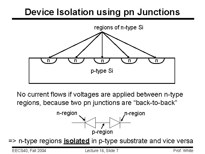
Device Isolation using pn Junctions regions of n-type Si n n n p-type Si No current flows if voltages are applied between n-type regions, because two pn junctions are “back-to-back” n-region p-region => n-type regions isolated in p-type substrate and vice versa EECS 40, Fall 2004 Lecture 16, Slide 7 Prof. White
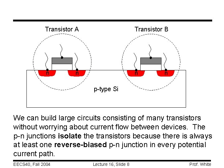
Transistor A Transistor B n n p-type Si We can build large circuits consisting of many transistors without worrying about current flow between devices. The p-n junctions isolate the transistors because there is always at least one reverse-biased p-n junction in every potential current path. EECS 40, Fall 2004 Lecture 16, Slide 8 Prof. White
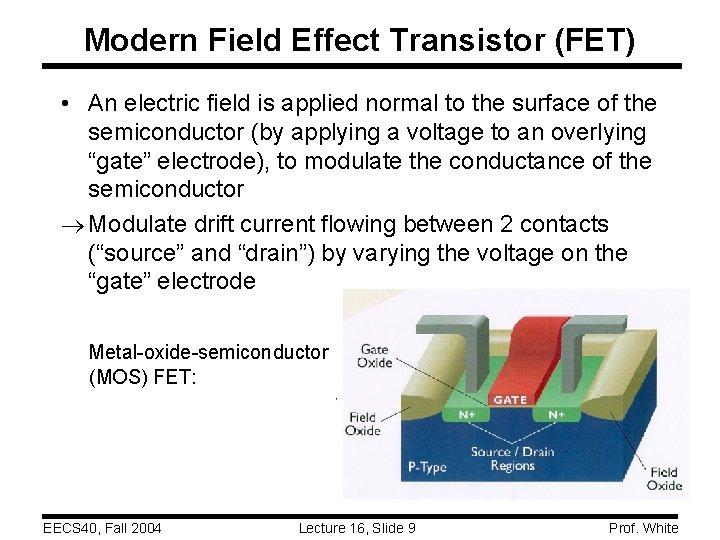
Modern Field Effect Transistor (FET) • An electric field is applied normal to the surface of the semiconductor (by applying a voltage to an overlying “gate” electrode), to modulate the conductance of the semiconductor ® Modulate drift current flowing between 2 contacts (“source” and “drain”) by varying the voltage on the “gate” electrode Metal-oxide-semiconductor (MOS) FET: EECS 40, Fall 2004 Lecture 16, Slide 9 Prof. White
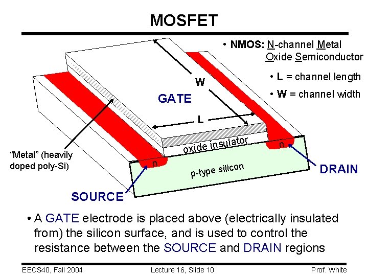
MOSFET • NMOS: N-channel Metal Oxide Semiconductor • L = channel length W • W = channel width GATE L lator “Metal” (heavily doped poly-Si) su oxide in n con ili p-type s n DRAIN SOURCE • A GATE electrode is placed above (electrically insulated from) the silicon surface, and is used to control the resistance between the SOURCE and DRAIN regions EECS 40, Fall 2004 Lecture 16, Slide 10 Prof. White
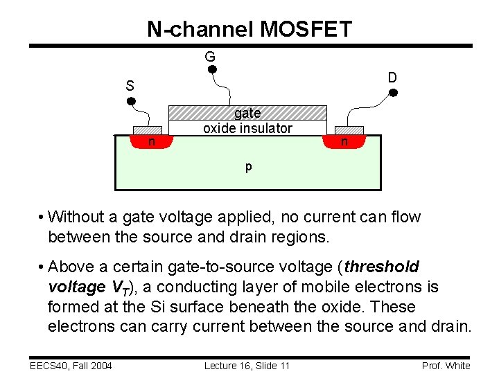
N-channel MOSFET G D S n gate oxide insulator n p • Without a gate voltage applied, no current can flow between the source and drain regions. • Above a certain gate-to-source voltage (threshold voltage VT), a conducting layer of mobile electrons is formed at the Si surface beneath the oxide. These electrons can carry current between the source and drain. EECS 40, Fall 2004 Lecture 16, Slide 11 Prof. White
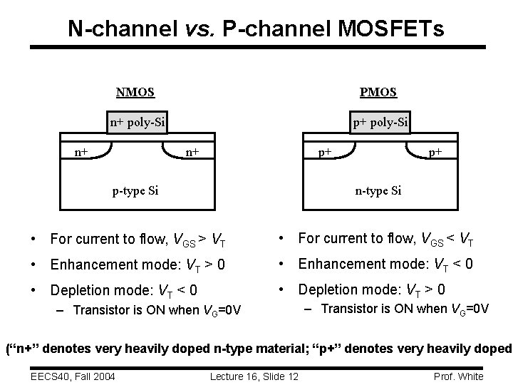
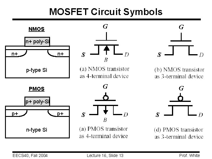
N-channel vs. P-channel MOSFETs NMOS PMOS n+ poly-Si p+ poly-Si n+ n+ p+ p-type Si p+ n-type Si • For current to flow, VGS > VT • For current to flow, VGS < VT • Enhancement mode: VT > 0 • Enhancement mode: VT < 0 • Depletion mode: VT > 0 – Transistor is ON when VG=0 V (“n+” denotes very heavily doped n-type material; “p+” denotes very heavily doped EECS 40, Fall 2004 Lecture 16, Slide 12 Prof. White
MOSFET Circuit Symbols G NMOS G n+ poly-Si n+ n+ S S p-type Si G PMOS G p+ poly-Si p+ p+ S S n-type Si EECS 40, Fall 2004 Lecture 16, Slide 13 Prof. White
Water Model for P-channel MOSFET EECS 40, Fall 2004 Lecture 16, Slide 14 Prof. White
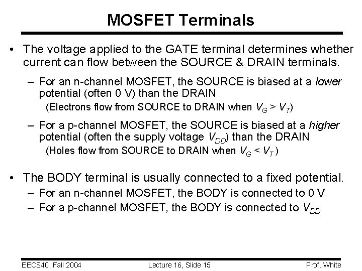
MOSFET Terminals • The voltage applied to the GATE terminal determines whether current can flow between the SOURCE & DRAIN terminals. – For an n-channel MOSFET, the SOURCE is biased at a lower potential (often 0 V) than the DRAIN (Electrons flow from SOURCE to DRAIN when VG > VT) – For a p-channel MOSFET, the SOURCE is biased at a higher potential (often the supply voltage VDD) than the DRAIN (Holes flow from SOURCE to DRAIN when VG < VT ) • The BODY terminal is usually connected to a fixed potential. – For an n-channel MOSFET, the BODY is connected to 0 V – For a p-channel MOSFET, the BODY is connected to VDD EECS 40, Fall 2004 Lecture 16, Slide 15 Prof. White
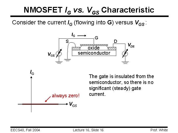
NMOSFET IG vs. VGS Characteristic Consider the current IG (flowing into G) versus VGS : IG G S oxide semiconductor VGS + IG always zero! D VDS + The gate is insulated from the semiconductor, so there is no significant (steady) gate current. VGS EECS 40, Fall 2004 Lecture 16, Slide 16 Prof. White
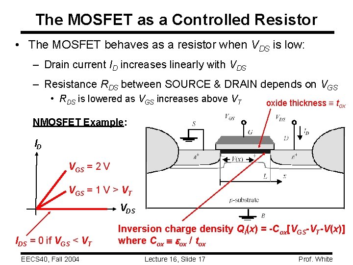
The MOSFET as a Controlled Resistor • The MOSFET behaves as a resistor when VDS is low: – Drain current ID increases linearly with VDS – Resistance RDS between SOURCE & DRAIN depends on VGS • RDS is lowered as VGS increases above VT oxide thickness tox NMOSFET Example: ID VGS = 2 V VGS = 1 V > VT VDS IDS = 0 if VGS < VT EECS 40, Fall 2004 Inversion charge density Qi(x) = -Cox[VGS-VT-V(x)] where Cox eox / tox Lecture 16, Slide 17 Prof. White
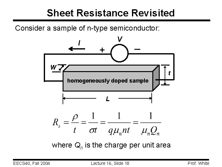
Sheet Resistance Revisited Consider a sample of n-type semiconductor: V I _ + W t homogeneously doped sample L where Qn is the charge per unit area EECS 40, Fall 2004 Lecture 16, Slide 18 Prof. White
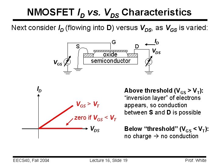
NMOSFET ID vs. VDS Characteristics Next consider ID (flowing into D) versus VDS, as VGS is varied: G S VGS + VGS > VT zero if VGS < VT VDS EECS 40, Fall 2004 D oxide semiconductor ID ID VDS + Above threshold (VGS > VT): “inversion layer” of electrons appears, so conduction between S and D is possible Below “threshold” (VGS < VT): no charge no conduction Lecture 16, Slide 19 Prof. White
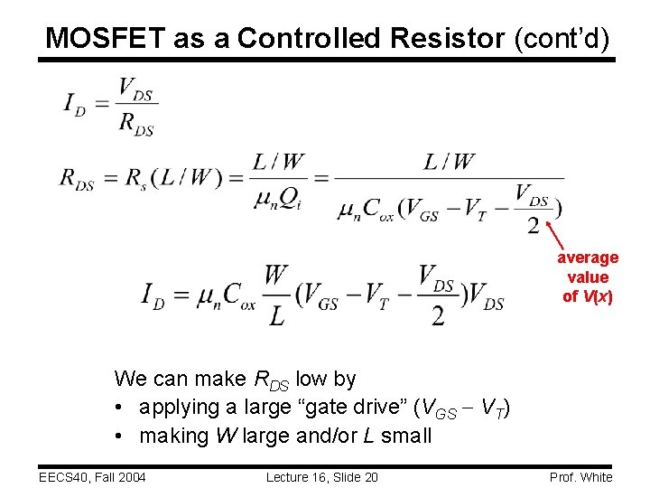
MOSFET as a Controlled Resistor (cont’d) average value of V(x) We can make RDS low by • applying a large “gate drive” (VGS VT) • making W large and/or L small EECS 40, Fall 2004 Lecture 16, Slide 20 Prof. White
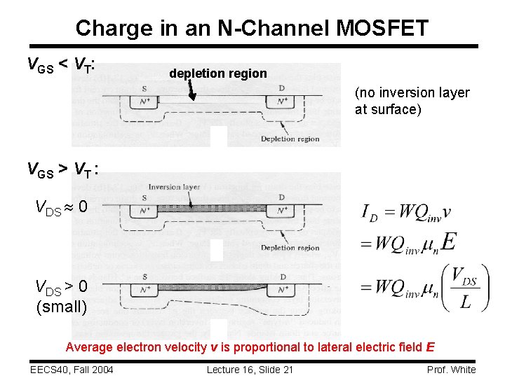
Charge in an N-Channel MOSFET VGS < VT: depletion region (no inversion layer at surface) VGS > VT : VDS 0 VDS > 0 (small) Average electron velocity v is proportional to lateral electric field E EECS 40, Fall 2004 Lecture 16, Slide 21 Prof. White
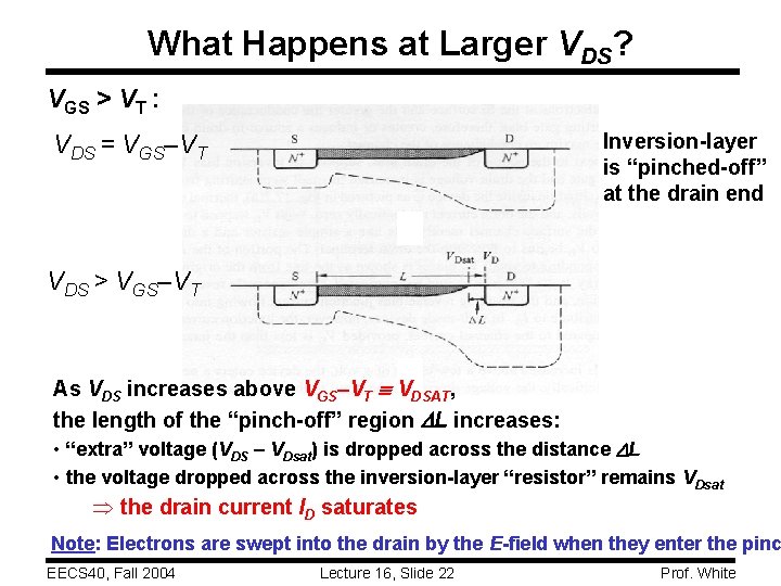
What Happens at Larger VDS? VGS > VT : Inversion-layer is “pinched-off” at the drain end VDS = VGS–VT VDS > VGS–VT As VDS increases above VGS–VT VDSAT, the length of the “pinch-off” region DL increases: • “extra” voltage (VDS – VDsat) is dropped across the distance DL • the voltage dropped across the inversion-layer “resistor” remains VDsat Þ the drain current ID saturates Note: Electrons are swept into the drain by the E-field when they enter the pinc EECS 40, Fall 2004 Lecture 16, Slide 22 Prof. White
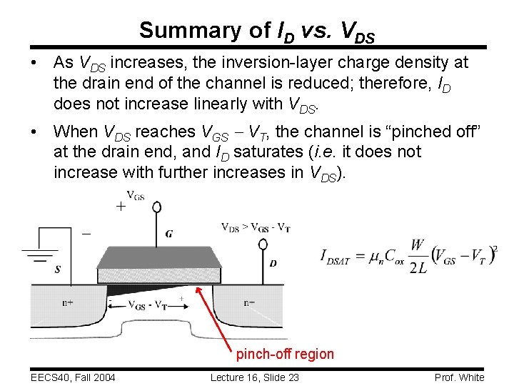
Summary of ID vs. VDS • As VDS increases, the inversion-layer charge density at the drain end of the channel is reduced; therefore, ID does not increase linearly with VDS. • When VDS reaches VGS VT, the channel is “pinched off” at the drain end, and ID saturates (i. e. it does not increase with further increases in VDS). + – pinch-off region EECS 40, Fall 2004 Lecture 16, Slide 23 Prof. White
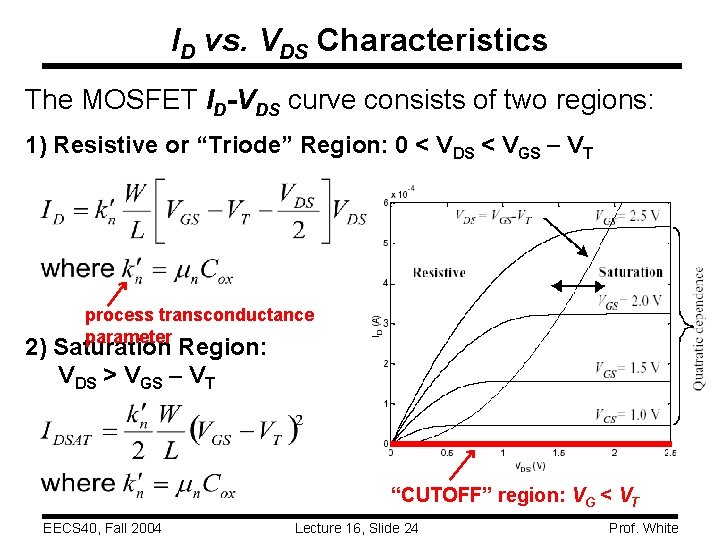
ID vs. VDS Characteristics The MOSFET ID-VDS curve consists of two regions: 1) Resistive or “Triode” Region: 0 < VDS < VGS VT process transconductance parameter 2) Saturation Region: VDS > VGS VT “CUTOFF” region: VG < VT EECS 40, Fall 2004 Lecture 16, Slide 24 Prof. White
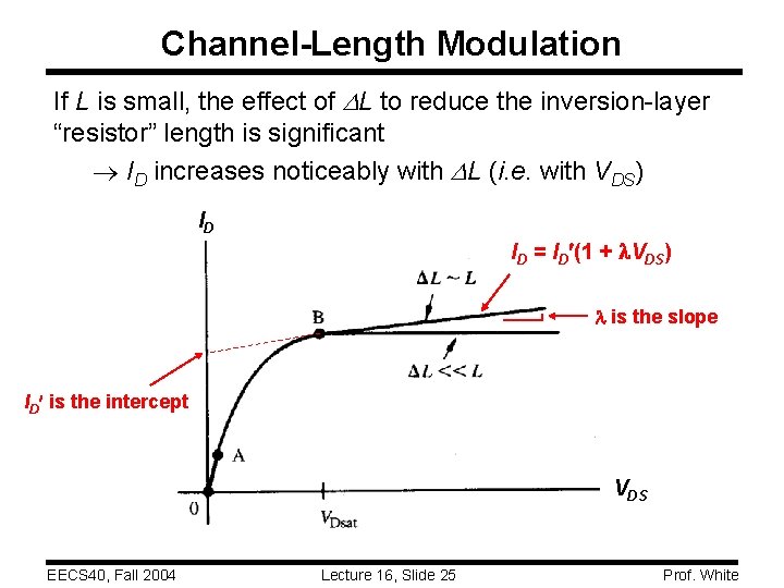
Channel-Length Modulation If L is small, the effect of DL to reduce the inversion-layer “resistor” length is significant ® ID increases noticeably with DL (i. e. with VDS) ID ID = ID (1 + l. VDS) l is the slope ID is the intercept VDS EECS 40, Fall 2004 Lecture 16, Slide 25 Prof. White
Velocity Saturation At high electric fields, the average velocity of carriers is NOT proportional to the field; it saturates at ~107 cm/sec for both electrons and holes: EECS 40, Fall 2004 Lecture 16, Slide 26 Prof. White
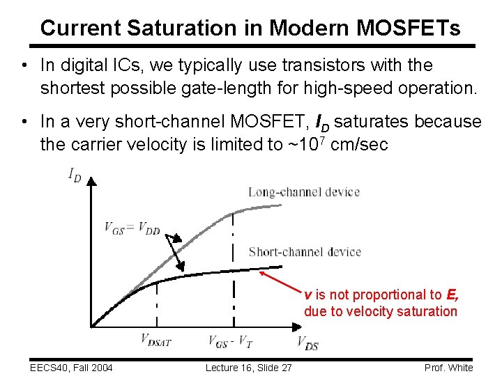
Current Saturation in Modern MOSFETs • In digital ICs, we typically use transistors with the shortest possible gate-length for high-speed operation. • In a very short-channel MOSFET, ID saturates because the carrier velocity is limited to ~107 cm/sec v is not proportional to E, due to velocity saturation EECS 40, Fall 2004 Lecture 16, Slide 27 Prof. White
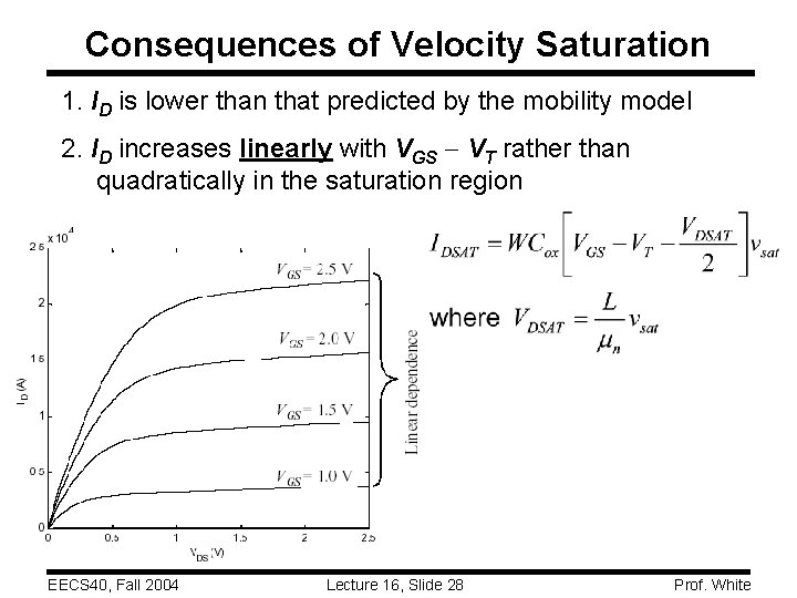
Consequences of Velocity Saturation 1. ID is lower than that predicted by the mobility model 2. ID increases linearly with VGS VT rather than quadratically in the saturation region EECS 40, Fall 2004 Lecture 16, Slide 28 Prof. White
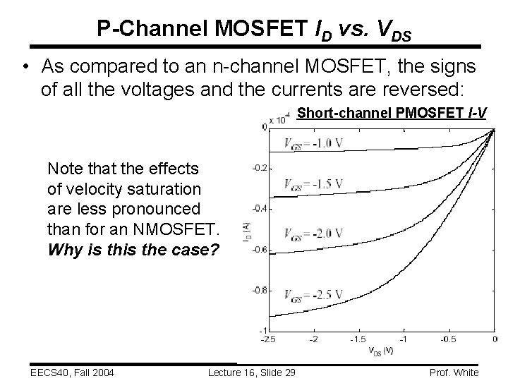
P-Channel MOSFET ID vs. VDS • As compared to an n-channel MOSFET, the signs of all the voltages and the currents are reversed: Short-channel PMOSFET I-V Note that the effects of velocity saturation are less pronounced than for an NMOSFET. Why is the case? EECS 40, Fall 2004 Lecture 16, Slide 29 Prof. White