LECTURE 16 Clocks Sequential circuit design The basic
LECTURE 16: • Clocks • Sequential circuit design • The basic memory element: a latch • Flip Flops
Clocks • Just about like everything else in this world, many digital logic designs “run on the clock” • Digital circuit designs that use a clock are called synchronous circuits • The clock synchronizes when things happen in the digital circuit
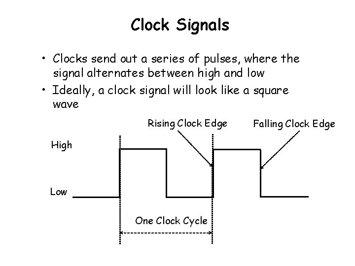
Clock Signals • Clocks send out a series of pulses, where the signal alternates between high and low • Ideally, a clock signal will look like a square wave Rising Clock Edge High Low One Clock Cycle Falling Clock Edge
Synchronous Digital Circuits • Synchronous digital circuits operation can be thought of as a series of discrete events • The clock is used to trigger these discrete events • Clock “triggers” can be: – Rising clock edge – Falling clock edge – Clock low – Clock high
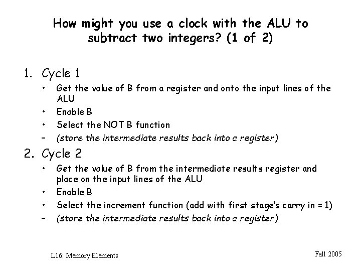
How might you use a clock with the ALU to subtract two integers? (1 of 2) 1. Cycle 1 • • • – Get the value of B from a register and onto the input lines of the ALU Enable B Select the NOT B function (store the intermediate results back into a register) 2. Cycle 2 • • • – Get the value of B from the intermediate results register and place on the input lines of the ALU Enable B Select the increment function (add with first stage’s carry in = 1) (store the intermediate results back into a register) L 16: Memory Elements Fall 2005
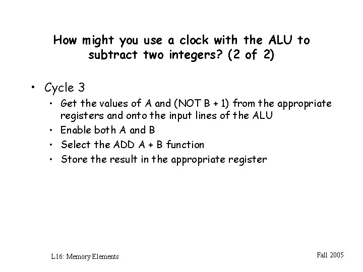
How might you use a clock with the ALU to subtract two integers? (2 of 2) • Cycle 3 • Get the values of A and (NOT B + 1) from the appropriate registers and onto the input lines of the ALU • Enable both A and B • Select the ADD A + B function • Store the result in the appropriate register L 16: Memory Elements Fall 2005
Memory and Sequential Logic • Memory allows us to store information so that we can use that information in the future • When we include memory in a circuit design, we call that type of circuit SEQUENTIAL LOGIC • In digital electronic circuits, a memory element can store a single value, either a “ 0” or a “ 1” • To enter a value into an memory element is called “writing” to memory • Retrieving a value that is stored in memory is called “reading” memory
Memory, Sequential Logic and Clocks • Memory functions and sequential logic have a sense of time (they remember what has happened before) • Memory functions and sequential logic are generally associated with the use of clocks • To enter a value into an memory element is called “writing” to memory • Retrieving a value that is stored in memory is called “reading” memory
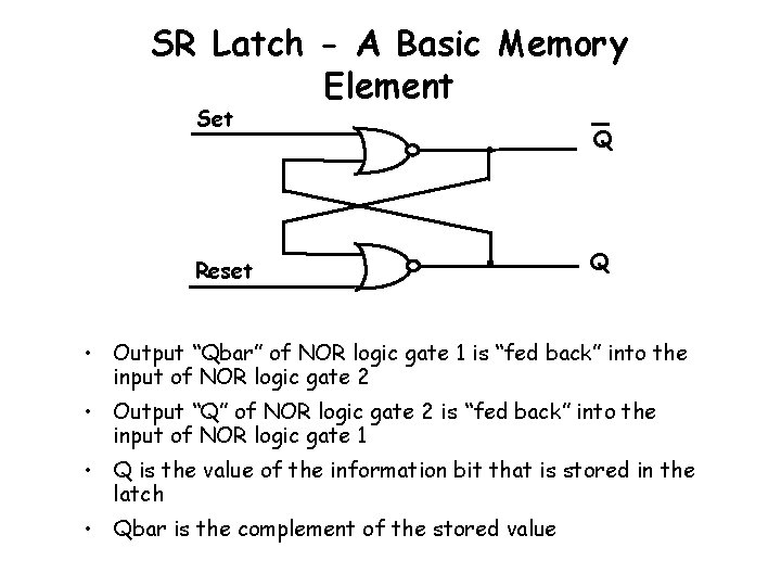
SR Latch - A Basic Memory Element Set Reset Q Q • Output “Qbar” of NOR logic gate 1 is “fed back” into the input of NOR logic gate 2 • Output “Q” of NOR logic gate 2 is “fed back” into the input of NOR logic gate 1 • Q is the value of the information bit that is stored in the latch • Qbar is the complement of the stored value
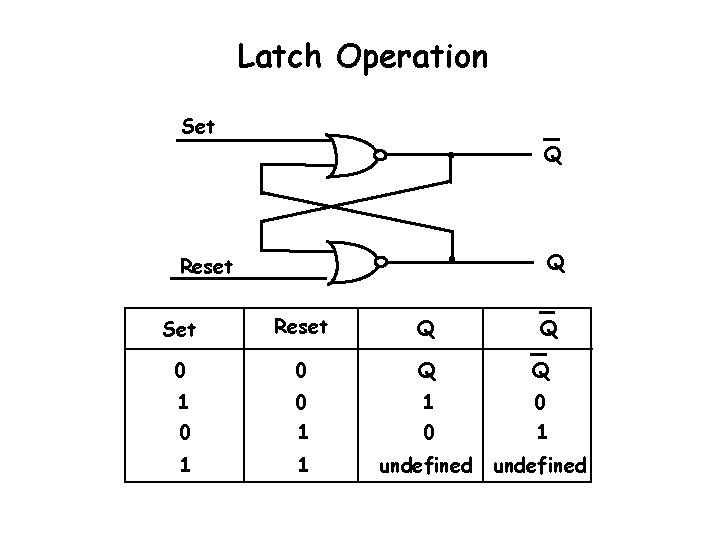
Latch Operation Set Q Q Reset Set Reset Q 0 0 Q Q 1 0 0 1 1 1 undefined Q
Storing Data in a Latch • The SR latch will keep the data (Q and Qbar) in its “last known” state for as long as set and reset are both zero • When a latch is first powered up, you don’t know which of its two stable states it will initialize to (with set=reset=0) One of the reasons why we initialize variables when we develop software
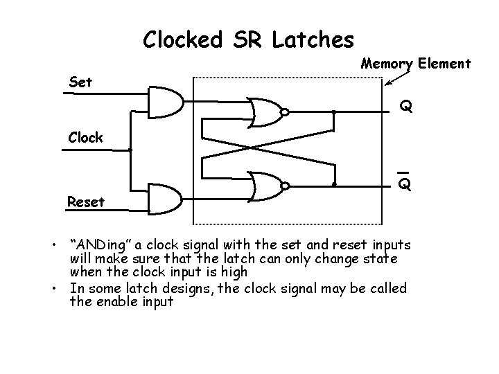
Clocked SR Latches Set Memory Element Q Clock Reset Q • “ANDing” a clock signal with the set and reset inputs will make sure that the latch can only change state when the clock input is high • In some latch designs, the clock signal may be called the enable input
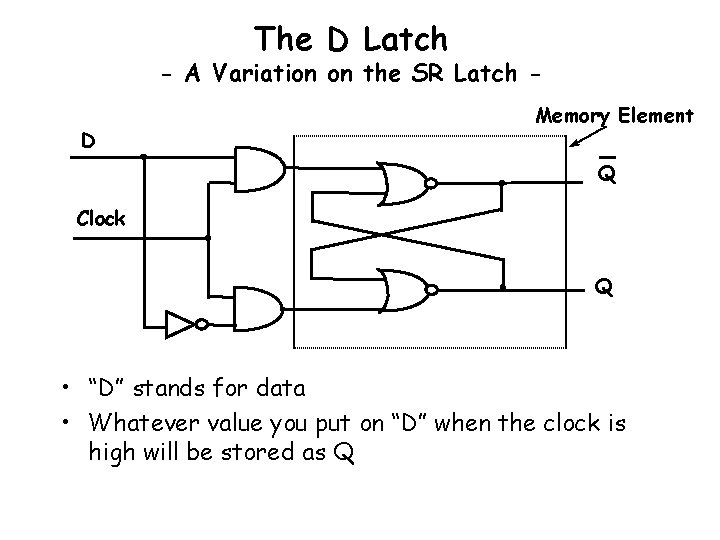
The D Latch - A Variation on the SR Latch D Memory Element Q Clock Q • “D” stands for data • Whatever value you put on “D” when the clock is high will be stored as Q
Latches vs. Flip-Flops • Latches are LEVEL-TRIGGERED The data (D) input to the latch is entered only when the clock input is “ 1” (“HIGH”) • Flip-flops are EDGE-TRIGGERED The data (D) input to the flip-flop is entered during a clock transition from either highto-low or low-to-high (i. e. , a clock edge)
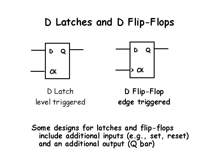
D Latches and D Flip-Flops D Q CK D Latch level triggered D > Q CK D Flip-Flop edge triggered Some designs for latches and flip-flops include additional inputs (e. g. , set, reset) and an additional output (Q bar)
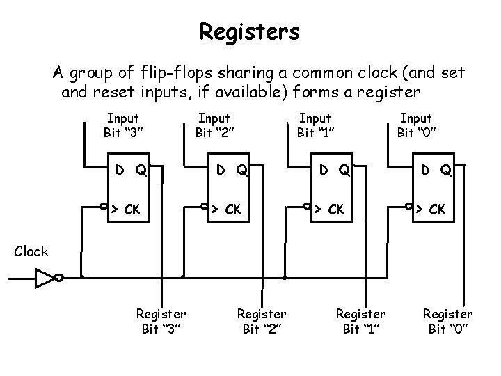
Registers A group of flip-flops sharing a common clock (and set and reset inputs, if available) forms a register Input Bit “ 3” D Q > CK Input Bit “ 2” Input Bit “ 1” D Q > CK Input Bit “ 0” D Q > CK Clock Register Bit “ 3” Register Bit “ 2” Register Bit “ 1” Register Bit “ 0”
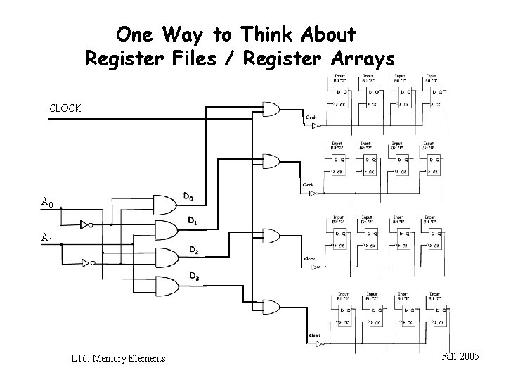
One Way to Think About Register Files / Register Arrays CLOCK A 0 A 1 L 16: Memory Elements Fall 2005
An Example of How Registers Might Work with an ALU • Assume that we want to add the values of two variables stored in registers (register 0 and register 1) and place the result in register 2 ADD R 0, R 1, R 2 • Assume that we have four, four-bit registers and a 4 bit ALU • Assume that Register 0 contains 0011 and that Register 1 contains 0010 • Process - synchronized by the clock signal: – Take the contents of the registers (R 0 and R 1) and load them into the ALU – Have the ALU add them (result = 0101) – Store the result back in the register (R 2)
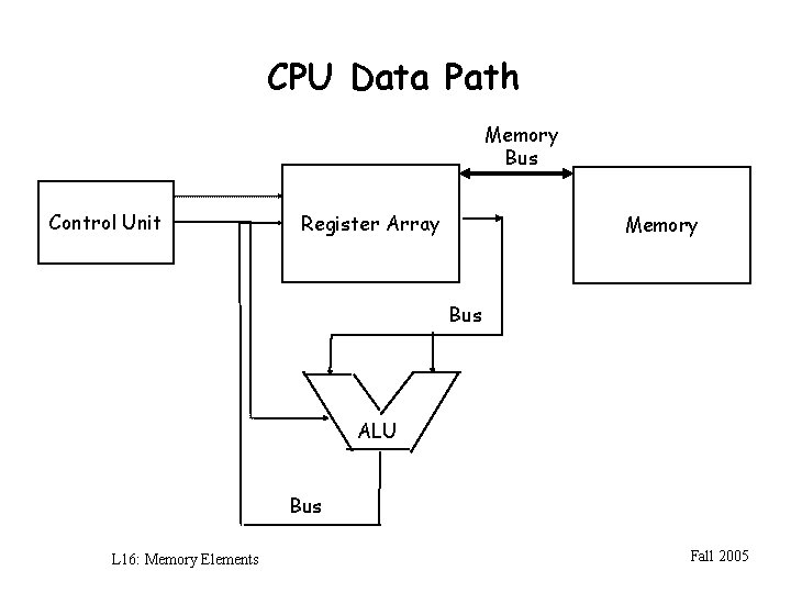
CPU Data Path Memory Bus Control Unit Register Array Memory Bus ALU Bus L 16: Memory Elements Fall 2005
- Slides: 19