Lecture 16 ANNOUNCEMENTS Wed discussion section Eudean Sun
- Slides: 20

Lecture 16 ANNOUNCEMENTS • Wed. discussion section (Eudean Sun) moved to 2 -3 PM in 293 Cory • HW#9 is posted online. OUTLINE • MOS capacitor (cont’d) – Effect of channel-to-body bias – Small-signal capacitance – PMOS capacitor • NMOSFET in ON state – Derivation of I-V characteristics – Regions of operation Reading: Chapter 6. 2. 2 EE 105 Fall 2007 Lecture 16, Slide 1 Prof. Liu, UC Berkeley

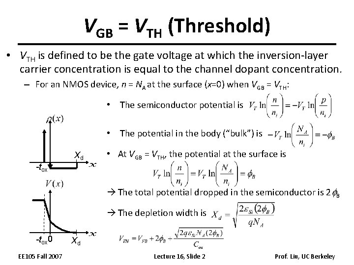
VGB = VTH (Threshold) • VTH is defined to be the gate voltage at which the inversion-layer carrier concentration is equal to the channel dopant concentration. – For an NMOS device, n = NA at the surface (x=0) when VGB = VTH: • The semiconductor potential is • The potential in the body (“bulk”) is Xd • At VGB = VTH, the potential at the surface is -tox The total potential dropped in the semiconductor is 2 f. B The depletion width is -tox 0 EE 105 Fall 2007 Xd Lecture 16, Slide 2 Prof. Liu, UC Berkeley

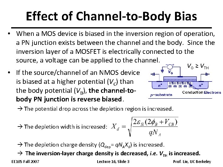
Effect of Channel-to-Body Bias • When a MOS device is biased in the inversion region of operation, a PN junction exists between the channel and the body. Since the inversion layer of a MOSFET is electrically connected to the source, a voltage can be applied to the channel. VG ≥ VTH • If the source/channel of an NMOS device is biased at a higher potential (VC) than the body potential (VB), the channel-tobody PN junction is reverse biased. The potential drop across the depletion region is increased. The depletion width is increased: The depletion charge density (Qdep= q. NAXd) is increased. The inversion-layer charge density is decreased, i. e. VTH is increased. EE 105 Fall 2007 Lecture 16, Slide 3 Prof. Liu, UC Berkeley

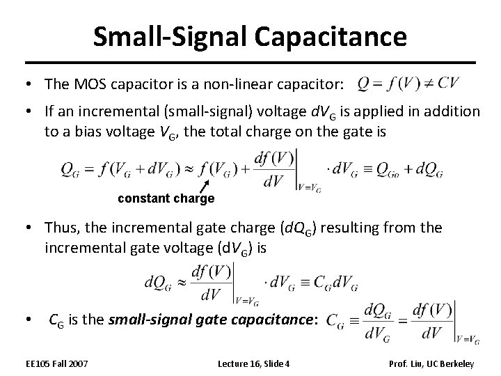
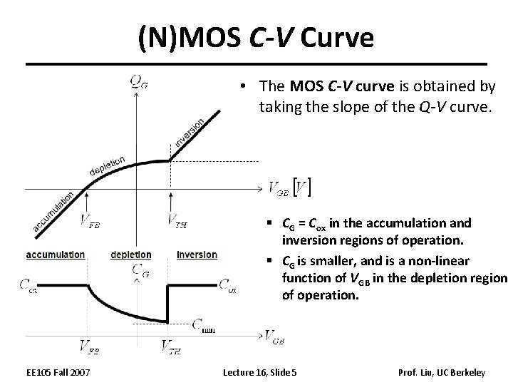
Small-Signal Capacitance • The MOS capacitor is a non-linear capacitor: • If an incremental (small-signal) voltage d. VG is applied in addition to a bias voltage VG, the total charge on the gate is constant charge • Thus, the incremental gate charge (d. QG) resulting from the incremental gate voltage (d. VG) is • CG is the small-signal gate capacitance: EE 105 Fall 2007 Lecture 16, Slide 4 Prof. Liu, UC Berkeley

(N)MOS C-V Curve • The MOS C-V curve is obtained by taking the slope of the Q-V curve. § CG = Cox in the accumulation and inversion regions of operation. § CG is smaller, and is a non-linear function of VGB in the depletion region of operation. EE 105 Fall 2007 Lecture 16, Slide 5 Prof. Liu, UC Berkeley

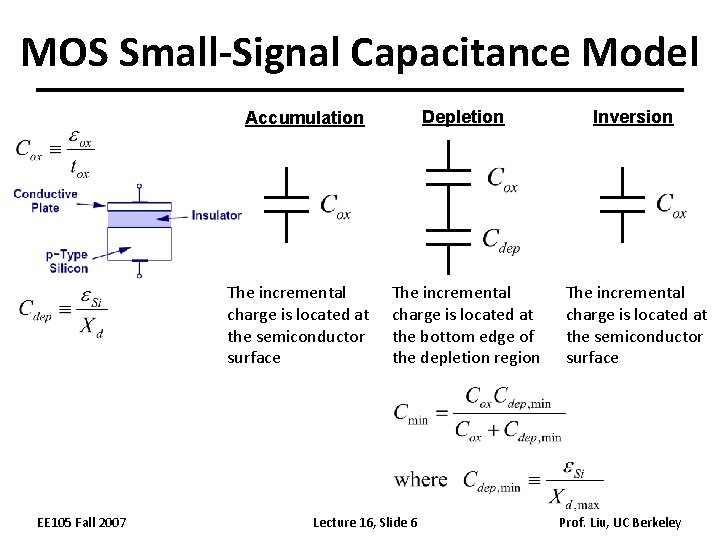
MOS Small-Signal Capacitance Model Depletion Inversion The incremental charge is located at the bottom edge of the depletion region The incremental charge is located at the semiconductor surface Accumulation The incremental charge is located at the semiconductor surface EE 105 Fall 2007 Lecture 16, Slide 6 Prof. Liu, UC Berkeley

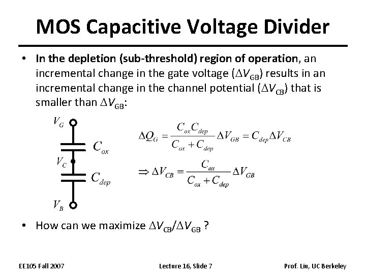
MOS Capacitive Voltage Divider • In the depletion (sub-threshold) region of operation, an incremental change in the gate voltage (DVGB) results in an incremental change in the channel potential (DVCB) that is smaller than DVGB: • How can we maximize DVCB/DVGB ? EE 105 Fall 2007 Lecture 16, Slide 7 Prof. Liu, UC Berkeley

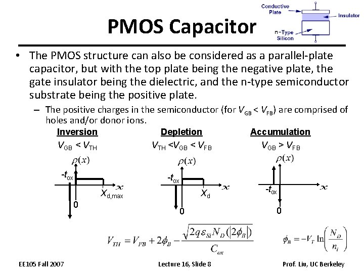
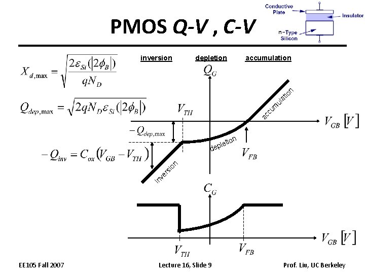
PMOS Capacitor • The PMOS structure can also be considered as a parallel-plate capacitor, but with the top plate being the negative plate, the gate insulator being the dielectric, and the n-type semiconductor substrate being the positive plate. – The positive charges in the semiconductor (for VGB < VFB) are comprised of holes and/or donor ions. Inversion VGB < VTH Depletion VTH <VGB < VFB -tox 0 EE 105 Fall 2007 Xd, max Xd 0 Lecture 16, Slide 8 Accumulation VGB > VFB -tox 0 Prof. Liu, UC Berkeley

PMOS Q-V , C-V depletion accumulation ac cu m ul at io n inversion eti l p e on in v er si o n d EE 105 Fall 2007 Lecture 16, Slide 9 Prof. Liu, UC Berkeley

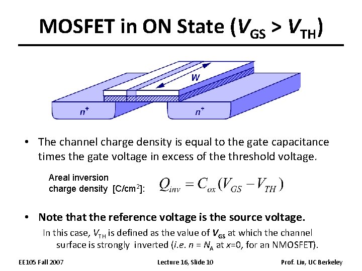
MOSFET in ON State (VGS > VTH) • The channel charge density is equal to the gate capacitance times the gate voltage in excess of the threshold voltage. Areal inversion charge density [C/cm 2]: • Note that the reference voltage is the source voltage. In this case, VTH is defined as the value of VGS at which the channel surface is strongly inverted (i. e. n = NA at x=0, for an NMOSFET). EE 105 Fall 2007 Lecture 16, Slide 10 Prof. Liu, UC Berkeley

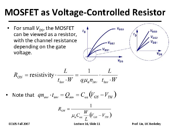
MOSFET as Voltage-Controlled Resistor • For small VDS, the MOSFET can be viewed as a resistor, with the channel resistance depending on the gate voltage. • Note that EE 105 Fall 2007 Lecture 16, Slide 11 Prof. Liu, UC Berkeley

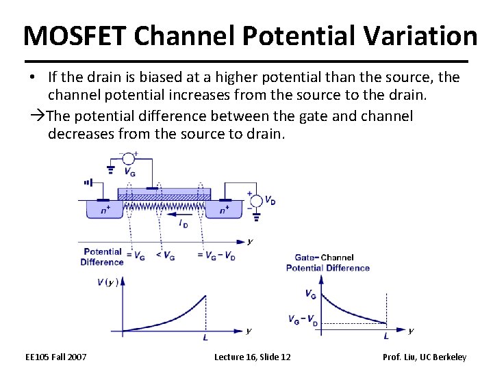
MOSFET Channel Potential Variation • If the drain is biased at a higher potential than the source, the channel potential increases from the source to the drain. The potential difference between the gate and channel decreases from the source to drain. EE 105 Fall 2007 Lecture 16, Slide 12 Prof. Liu, UC Berkeley

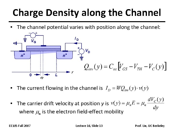
Charge Density along the Channel • The channel potential varies with position along the channel: • The current flowing in the channel is • The carrier drift velocity at position y is where mn is the electron field-effect mobility EE 105 Fall 2007 Lecture 16, Slide 13 Prof. Liu, UC Berkeley

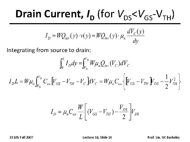
Drain Current, ID (for VDS<VGS-VTH) Integrating from source to drain: EE 105 Fall 2007 Lecture 16, Slide 14 Prof. Liu, UC Berkeley

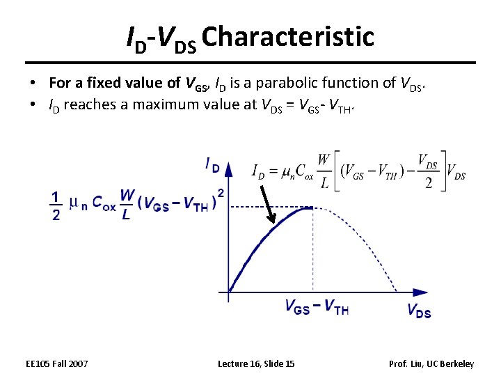
ID-VDS Characteristic • For a fixed value of VGS, ID is a parabolic function of VDS. • ID reaches a maximum value at VDS = VGS- VTH. EE 105 Fall 2007 Lecture 16, Slide 15 Prof. Liu, UC Berkeley

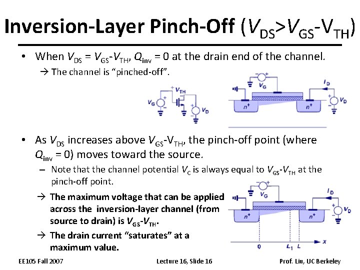
Inversion-Layer Pinch-Off (VDS>VGS-VTH) • When VDS = VGS-VTH, Qinv = 0 at the drain end of the channel. The channel is “pinched-off”. • As VDS increases above VGS-VTH, the pinch-off point (where Qinv = 0) moves toward the source. – Note that the channel potential VC is always equal to VGS-VTH at the pinch-off point. The maximum voltage that can be applied across the inversion-layer channel (from source to drain) is VGS-VTH. The drain current “saturates” at a maximum value. EE 105 Fall 2007 Lecture 16, Slide 16 Prof. Liu, UC Berkeley

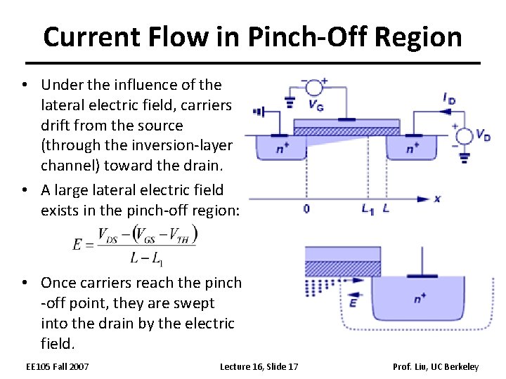
Current Flow in Pinch-Off Region • Under the influence of the lateral electric field, carriers drift from the source (through the inversion-layer channel) toward the drain. • A large lateral electric field exists in the pinch-off region: • Once carriers reach the pinch -off point, they are swept into the drain by the electric field. EE 105 Fall 2007 Lecture 16, Slide 17 Prof. Liu, UC Berkeley

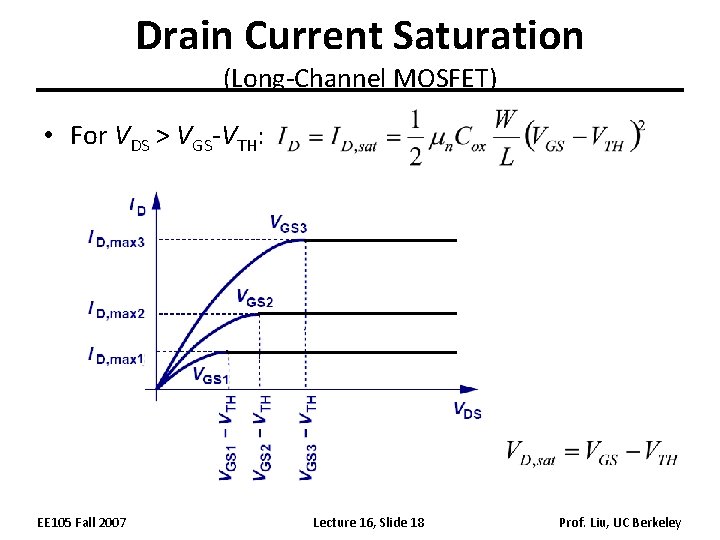
Drain Current Saturation (Long-Channel MOSFET) • For VDS > VGS-VTH: EE 105 Fall 2007 Lecture 16, Slide 18 Prof. Liu, UC Berkeley

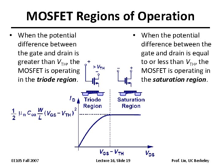
MOSFET Regions of Operation • When the potential difference between the gate and drain is greater than VTH, the MOSFET is operating in the triode region. EE 105 Fall 2007 • When the potential difference between the gate and drain is equal to or less than VTH, the MOSFET is operating in the saturation region. Lecture 16, Slide 19 Prof. Liu, UC Berkeley

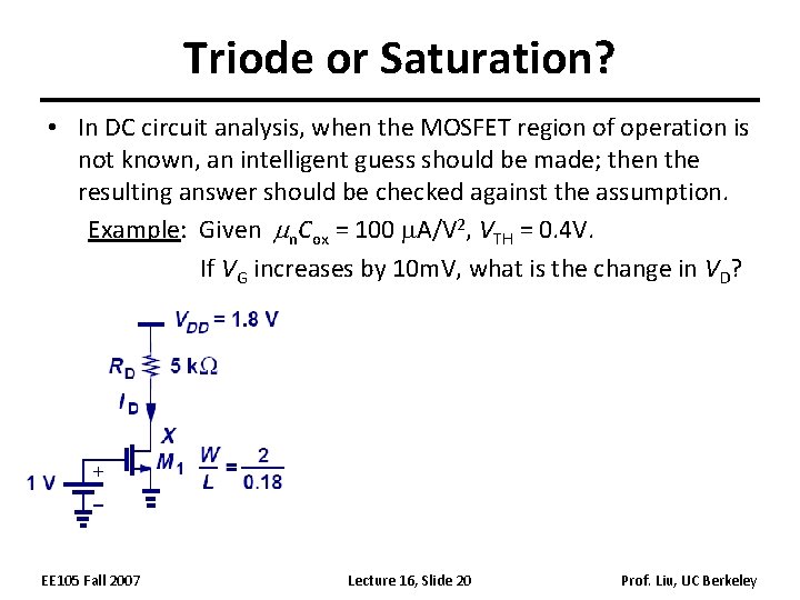
Triode or Saturation? • In DC circuit analysis, when the MOSFET region of operation is not known, an intelligent guess should be made; then the resulting answer should be checked against the assumption. Example: Given mn. Cox = 100 m. A/V 2, VTH = 0. 4 V. If VG increases by 10 m. V, what is the change in VD? EE 105 Fall 2007 Lecture 16, Slide 20 Prof. Liu, UC Berkeley