Lecture 14 alt Memory Test Alternative for Lecture
- Slides: 25

Lecture 14 alt Memory Test (Alternative for Lecture 15) § § § § Memory organization Memory test complexity Faults and fault models MATS+ march test Address Decoder faults Summary References Copyright 2005, Agrawal & Bushnell VLSI Test: Lecture 14 alt 1

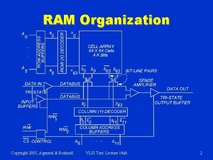
RAM Organization Copyright 2005, Agrawal & Bushnell VLSI Test: Lecture 14 alt 2

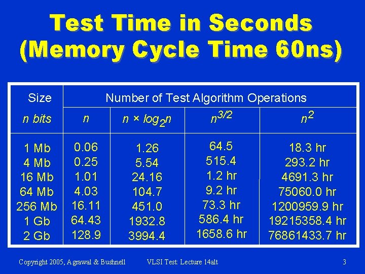
Test Time in Seconds (Memory Cycle Time 60 ns) Size Number of Test Algorithm Operations n bits n n × log 2 n n 3/2 n 2 1 Mb 4 Mb 16 Mb 64 Mb 256 Mb 1 Gb 2 Gb 0. 06 0. 25 1. 01 4. 03 16. 11 64. 43 128. 9 1. 26 5. 54 24. 16 104. 7 451. 0 1932. 8 3994. 4 64. 5 515. 4 1. 2 hr 9. 2 hr 73. 3 hr 586. 4 hr 1658. 6 hr 18. 3 hr 293. 2 hr 4691. 3 hr 75060. 0 hr 1200959. 9 hr 19215358. 4 hr 76861433. 7 hr Copyright 2005, Agrawal & Bushnell VLSI Test: Lecture 14 alt 3

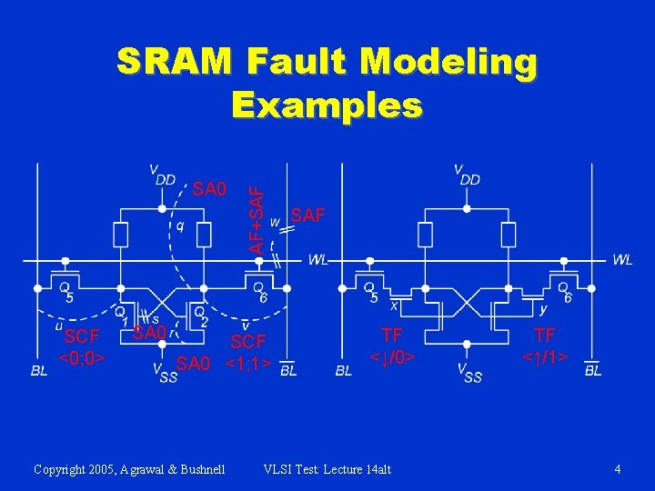
SA 0 SCF <0; 0> SA 0 AF+SAF SRAM Fault Modeling Examples SCF SA 0 <1; 1> Copyright 2005, Agrawal & Bushnell SAF TF <↓/0> VLSI Test: Lecture 14 alt TF <↑/1> 4

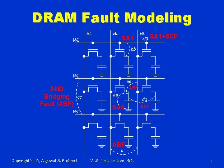
DRAM Fault Modeling SA 1+SCF SA 1 AND Bridging Fault (ABF) ABF SA 0 SCF ABF Copyright 2005, Agrawal & Bushnell VLSI Test: Lecture 14 alt 5

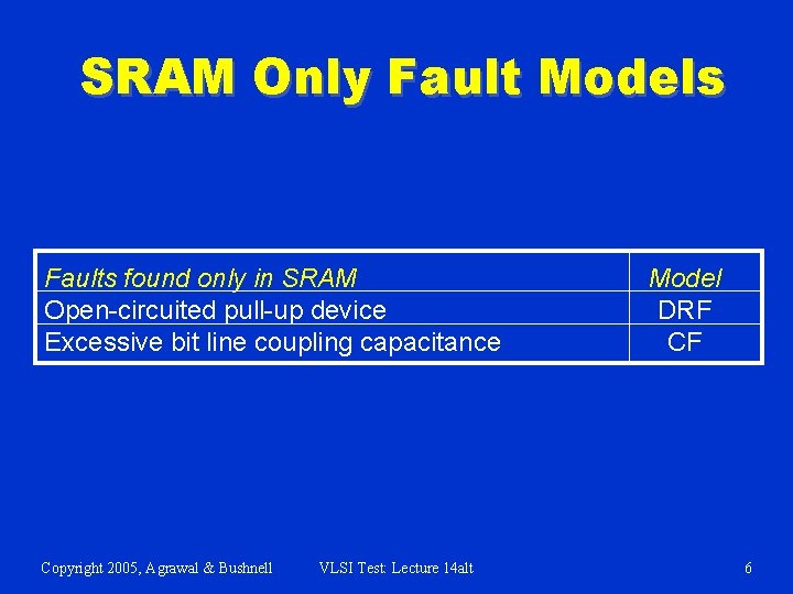
SRAM Only Fault Models Faults found only in SRAM Open-circuited pull-up device Excessive bit line coupling capacitance Copyright 2005, Agrawal & Bushnell VLSI Test: Lecture 14 alt Model DRF CF 6

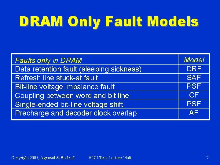
DRAM Only Fault Models Faults only in DRAM Data retention fault (sleeping sickness) Refresh line stuck-at fault Bit-line voltage imbalance fault Coupling between word and bit line Single-ended bit-line voltage shift Precharge and decoder clock overlap Copyright 2005, Agrawal & Bushnell VLSI Test: Lecture 14 alt Model DRF SAF PSF CF PSF AF 7

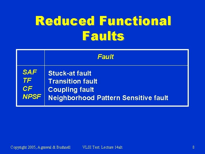
Reduced Functional Faults Fault SAF TF CF NPSF Stuck-at fault Transition fault Coupling fault Neighborhood Pattern Sensitive fault Copyright 2005, Agrawal & Bushnell VLSI Test: Lecture 14 alt 8

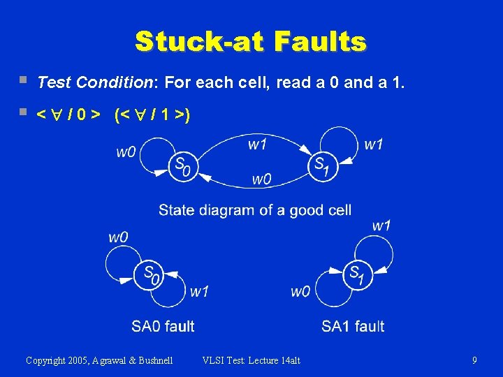
Stuck-at Faults § § Test Condition: For each cell, read a 0 and a 1. < / 0 > (< / 1 >) Copyright 2005, Agrawal & Bushnell VLSI Test: Lecture 14 alt 9

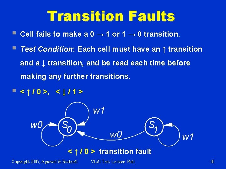
Transition Faults § § Cell fails to make a 0 → 1 or 1 → 0 transition. Test Condition: Each cell must have an ↑ transition and a ↓ transition, and be read each time before making any further transitions. § < ↑ / 0 >, < ↓ / 1 > < ↑ / 0 > transition fault Copyright 2005, Agrawal & Bushnell VLSI Test: Lecture 14 alt 10

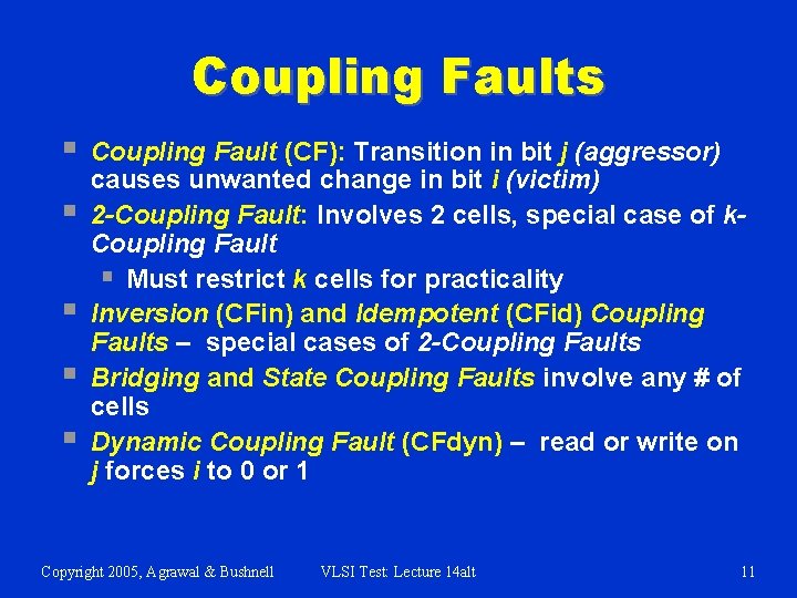
Coupling Faults § § § Coupling Fault (CF): Transition in bit j (aggressor) causes unwanted change in bit i (victim) 2 -Coupling Fault: Involves 2 cells, special case of k. Coupling Fault § Must restrict k cells for practicality Inversion (CFin) and Idempotent (CFid) Coupling Faults – special cases of 2 -Coupling Faults Bridging and State Coupling Faults involve any # of cells Dynamic Coupling Fault (CFdyn) – read or write on j forces i to 0 or 1 Copyright 2005, Agrawal & Bushnell VLSI Test: Lecture 14 alt 11

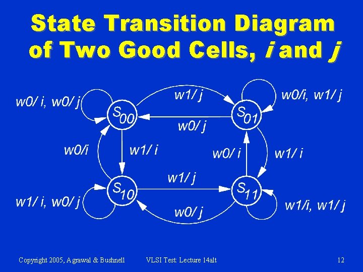
State Transition Diagram of Two Good Cells, i and j Copyright 2005, Agrawal & Bushnell VLSI Test: Lecture 14 alt 12

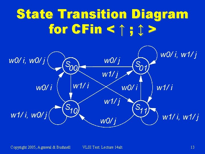
State Transition Diagram for CFin < ↑ ; ↕ > Copyright 2005, Agrawal & Bushnell VLSI Test: Lecture 14 alt 13

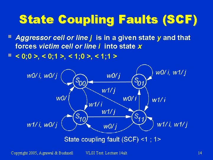
State Coupling Faults (SCF) § § Aggressor cell or line j is in a given state y and that forces victim cell or line i into state x < 0; 0 >, < 0; 1 >, < 1; 0 >, < 1; 1 > Copyright 2005, Agrawal & Bushnell VLSI Test: Lecture 14 alt 14

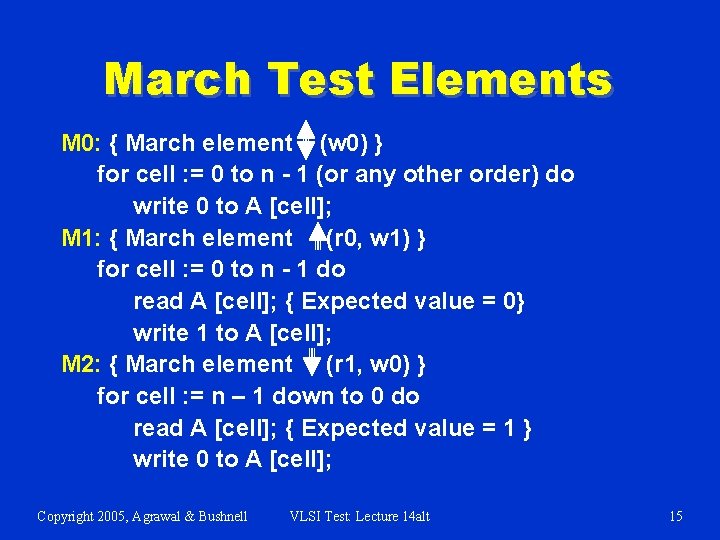
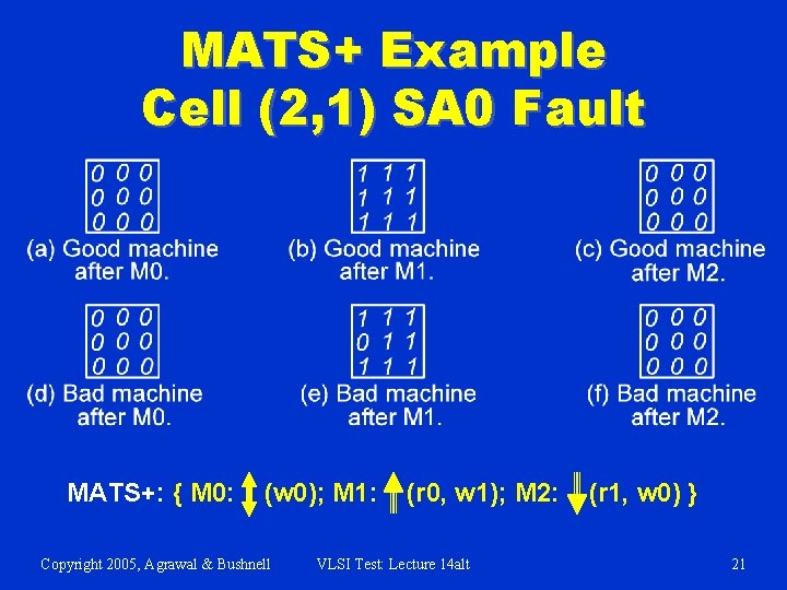
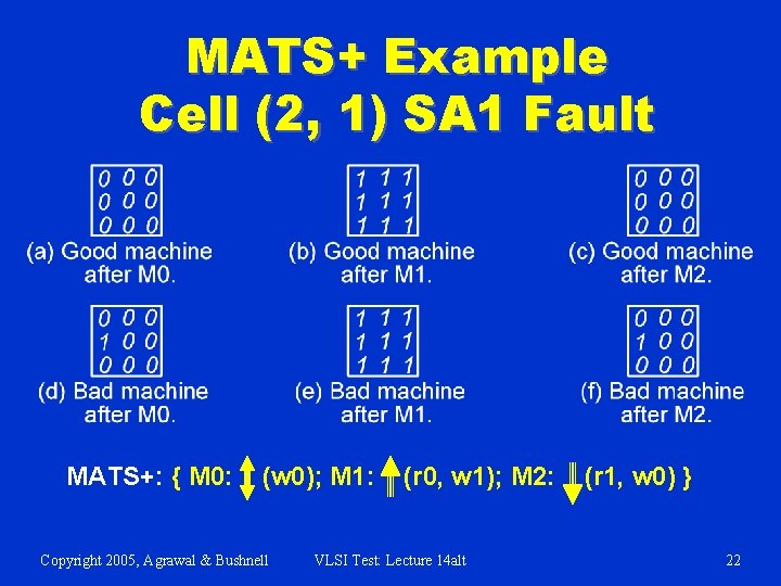
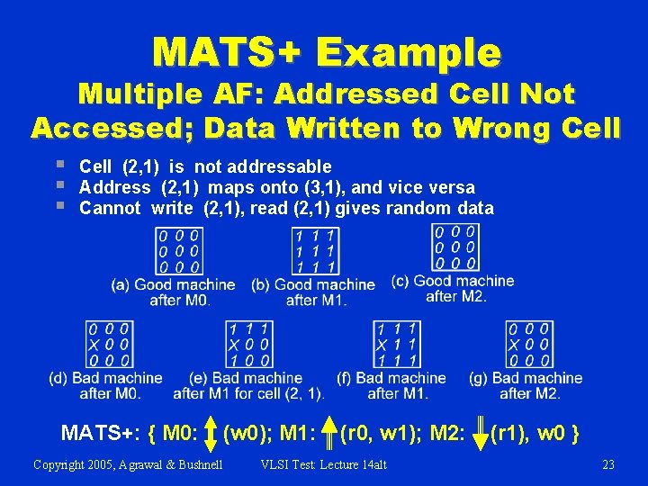
March Test Elements M 0: { March element (w 0) } for cell : = 0 to n - 1 (or any other order) do write 0 to A [cell]; M 1: { March element (r 0, w 1) } for cell : = 0 to n - 1 do read A [cell]; { Expected value = 0} write 1 to A [cell]; M 2: { March element (r 1, w 0) } for cell : = n – 1 down to 0 do read A [cell]; { Expected value = 1 } write 0 to A [cell]; Copyright 2005, Agrawal & Bushnell VLSI Test: Lecture 14 alt 15

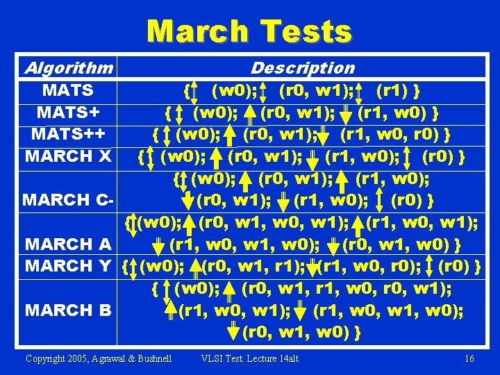
March Tests Algorithm MATS++ MARCH X (w 0); (r 0, w 1); (r 1) } { (w 0); (r 0, w 1); (r 1, w 0, r 0) } { (w 0); (r 0, w 1); (r 1, w 0); (r 0) } { (w 0); (r 0, w 1); (r 1, w 0); MARCH C(r 0, w 1); (r 1, w 0); (r 0) } { (w 0); (r 0, w 1, w 0, w 1); (r 1, w 0, w 1); MARCH A (r 1, w 0, w 1, w 0); (r 0, w 1, w 0) } MARCH Y { (w 0); (r 0, w 1, r 1); (r 1, w 0, r 0); (r 0) } { (w 0); (r 0, w 1, r 1, w 0, r 0, w 1); MARCH B (r 1, w 0, w 1); (r 1, w 0, w 1, w 0); (r 0, w 1, w 0) } Copyright 2005, Agrawal & Bushnell { Description VLSI Test: Lecture 14 alt 16

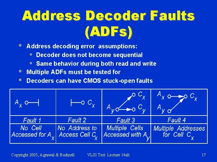
Address Decoder Faults (ADFs) § § § Address decoding error assumptions: § Decoder does not become sequential § Same behavior during both read and write Multiple ADFs must be tested for Decoders can have CMOS stuck-open faults Copyright 2005, Agrawal & Bushnell VLSI Test: Lecture 14 alt 17

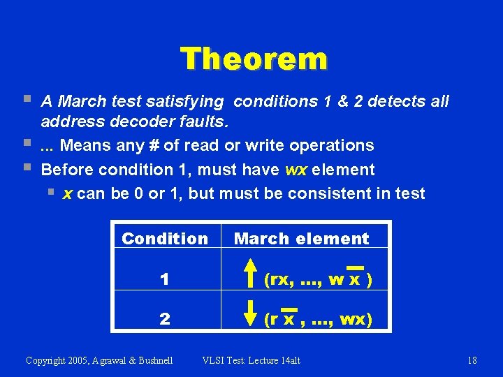
Theorem § § § A March test satisfying conditions 1 & 2 detects all address decoder faults. . Means any # of read or write operations Before condition 1, must have wx element § x can be 0 or 1, but must be consistent in test Condition March element 1 (rx, …, w x ) 2 (r x , …, wx) Copyright 2005, Agrawal & Bushnell VLSI Test: Lecture 14 alt 18

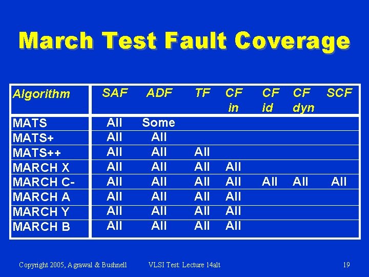
March Test Fault Coverage Algorithm SAF ADF TF MATS++ MARCH X MARCH CMARCH A MARCH Y MARCH B All All Some All All All All Copyright 2005, Agrawal & Bushnell VLSI Test: Lecture 14 alt CF in All All All CF id CF SCF dyn All All 19

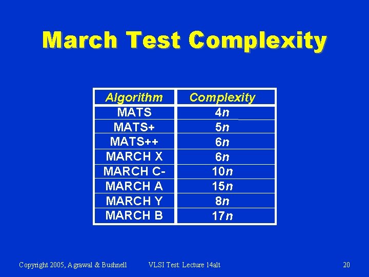
March Test Complexity Algorithm MATS++ MARCH X MARCH CMARCH A MARCH Y MARCH B Copyright 2005, Agrawal & Bushnell Complexity 4 n 5 n 6 n 6 n 10 n 15 n 8 n 17 n VLSI Test: Lecture 14 alt 20

MATS+ Example Cell (2, 1) SA 0 Fault MATS+: { M 0: (w 0); M 1: Copyright 2005, Agrawal & Bushnell (r 0, w 1); M 2: VLSI Test: Lecture 14 alt (r 1, w 0) } 21

MATS+ Example Cell (2, 1) SA 1 Fault MATS+: { M 0: (w 0); M 1: Copyright 2005, Agrawal & Bushnell (r 0, w 1); M 2: VLSI Test: Lecture 14 alt (r 1, w 0) } 22

MATS+ Example Multiple AF: Addressed Cell Not Accessed; Data Written to Wrong Cell § § § Cell (2, 1) is not addressable Address (2, 1) maps onto (3, 1), and vice versa Cannot write (2, 1), read (2, 1) gives random data MATS+: { M 0: (w 0); M 1: Copyright 2005, Agrawal & Bushnell (r 0, w 1); M 2: VLSI Test: Lecture 14 alt (r 1), w 0 } 23

Memory Test Summary § § § Multiple fault models are essential Combination of tests is essential: § March – SRAM and DRAM § NPSF – DRAM § DC Parametric – Both § AC Parametric – Both Related areas of memory test § BIST – standard practice for embedded memories § Repairable memories – redundancy to enhance yield Copyright 2005, Agrawal & Bushnell VLSI Test: Lecture 14 alt 24

References on Memory Test § § § § § R. D. Adams, High Performance Memory Testing, Boston: Springer, 2002. M. L. Bushnell and V. D. Agrawal, Essentials of Electronic Testing for Digital, Memory and Mixed-Signal VLSI Circuits, Boston: Springer, 2000. K. Chakraborty and P. Mazumder, Fault Tolerance and Reliability Techniques for High-Density Random-Access Memories, Upper Saddle River, New Jersey: Prentice Hall PTR, 2002. K. Chakraborty and P. Mazumder, Testing and Testable Design of High. Density Random-Access Memories, Boston: Springer, 1996. D. Gizopoulos, editor, Advances in Electronic Testing Challenges and Methodologies, Springer, 2006. S. Hamdioui, Testing Static Random Access Memories: Defects, Fault Models and Test Patterns, Springer, 2004. B. Prince, High Performance Memories, Revised Edition, Wiley, 1999. A. K. Sharma, Semiconductor Memories: Testing Technology, and Reliability, Piscataway, New Jersey: IEEE Press, 1997. A. J. van de Goor, Testing Semiconductor Memories, Chichester, UK: Wiley Interscience, 1991, reprinted by Com. Tex, Gouda, The Netherlands (http: //ce. et. tudelft. nl/vdgoor/). Copyright 2005, Agrawal & Bushnell VLSI Test: Lecture 14 alt 25