Lecture 12 Analog to Digital Converters Analog to






- Slides: 47

Lecture 12 Analog to Digital Converters

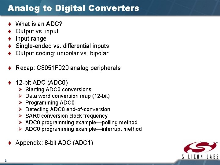
Analog to Digital Converters ¨ ¨ ¨ What is an ADC? Output vs. input Input range Single-ended vs. differential inputs Output coding: unipolar vs. bipolar ¨ Recap: C 8051 F 020 analog peripherals ¨ 12 -bit ADC (ADC 0) Ø Ø Ø Ø Starting ADC 0 conversions Data word conversion map (12 -bit) Programming ADC 0 Detecting ADC 0 end-of-conversion SAR 0 conversion clock frequency ADC 0 programming example—polling method ADC 0 programming example—interrupt method ¨ Appendix: 8 -bit ADC (ADC 1) 2

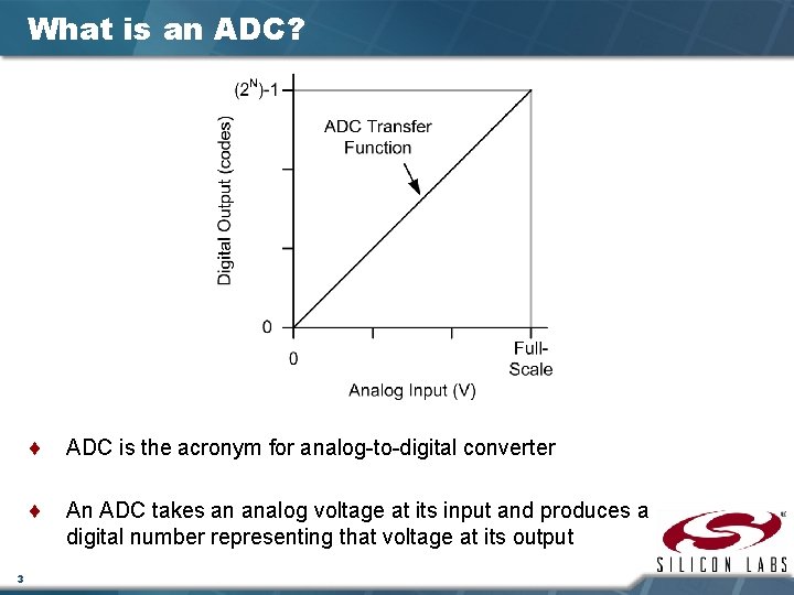
What is an ADC? 3 ¨ ADC is the acronym for analog-to-digital converter ¨ An ADC takes an analog voltage at its input and produces a digital number representing that voltage at its output

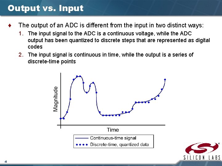
Output vs. Input ¨ The output of an ADC is different from the input in two distinct ways: 1. The input signal to the ADC is a continuous voltage, while the ADC output has been quantized to discrete steps that are represented as digital codes 2. The input signal is continuous in time, while the output is a series of discrete-time points 4

ADC—Input Range ¨ An ADC’s input range is defined by the reference voltage (VREF) provided to the ADC ¨ The power supplies to the ADC are also important in determining the absolute input voltage Ø In most ADC architectures, input voltages outside the supply rails cannot be measured and may cause damage to the device 5

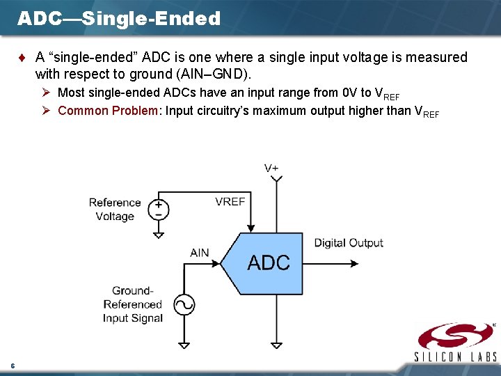
ADC—Single-Ended ¨ A “single-ended” ADC is one where a single input voltage is measured with respect to ground (AIN–GND). Ø Most single-ended ADCs have an input range from 0 V to VREF Ø Common Problem: Input circuitry’s maximum output higher than VREF 6

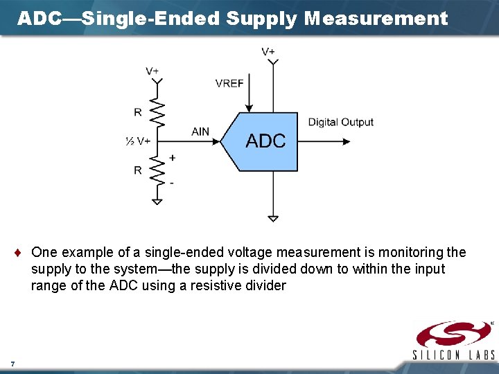
ADC—Single-Ended Supply Measurement ¨ One example of a single-ended voltage measurement is monitoring the supply to the system—the supply is divided down to within the input range of the ADC using a resistive divider 7

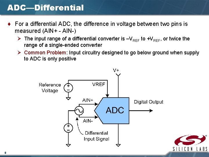
ADC—Differential ¨ For a differential ADC, the difference in voltage between two pins is measured (AIN+ - AIN-) Ø The input range of a differential converter is –VREF to +VREF, or twice the range of a single-ended converter Ø Common Problem: Input circuitry designed to go below ground when supply to ADC is only positive 8

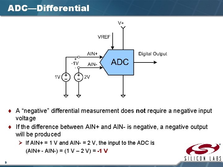
ADC—Differential ¨ A “negative” differential measurement does not require a negative input voltage ¨ If the difference between AIN+ and AIN- is negative, a negative output will be produced Ø If AIN+ = 1 V and AIN- = 2 V, the input to the ADC is (AIN+ - AIN-) = (1 V – 2 V) = -1 V 9

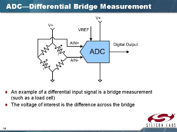
ADC—Differential Bridge Measurement ¨ An example of a differential input signal is a bridge measurement (such as a load cell) ¨ The voltage of interest is the difference across the bridge 10

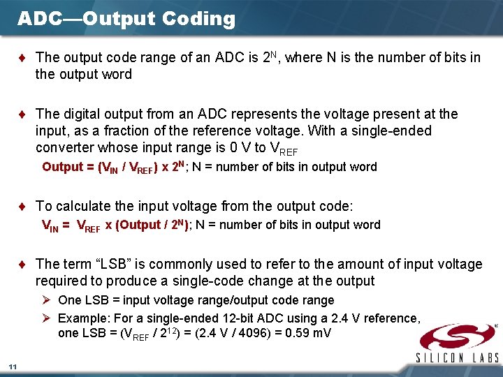
ADC—Output Coding ¨ The output code range of an ADC is 2 N, where N is the number of bits in the output word ¨ The digital output from an ADC represents the voltage present at the input, as a fraction of the reference voltage. With a single-ended converter whose input range is 0 V to VREF Output = (VIN / VREF) x 2 N; N = number of bits in output word ¨ To calculate the input voltage from the output code: VIN = VREF x (Output / 2 N); N = number of bits in output word ¨ The term “LSB” is commonly used to refer to the amount of input voltage required to produce a single-code change at the output Ø One LSB = input voltage range/output code range Ø Example: For a single-ended 12 -bit ADC using a 2. 4 V reference, one LSB = (VREF / 212) = (2. 4 V / 4096) = 0. 59 m. V 11

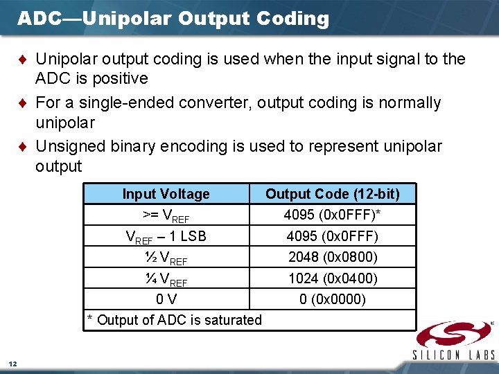
ADC—Unipolar Output Coding ¨ Unipolar output coding is used when the input signal to the ADC is positive ¨ For a single-ended converter, output coding is normally unipolar ¨ Unsigned binary encoding is used to represent unipolar output Input Voltage Output Code (12 -bit) >= VREF 4095 (0 x 0 FFF)* VREF – 1 LSB 4095 (0 x 0 FFF) ½ VREF 2048 (0 x 0800) ¼ VREF 1024 (0 x 0400) 0 V 0 (0 x 0000) * Output of ADC is saturated 12

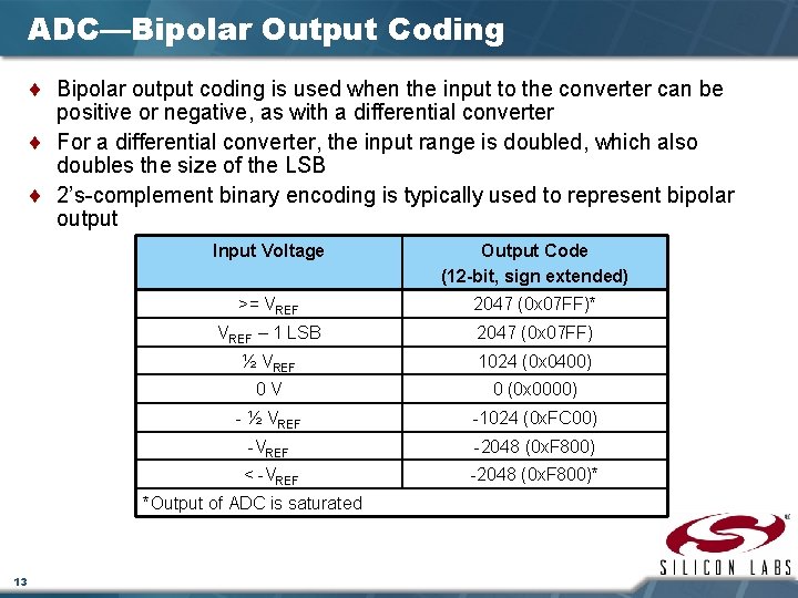
ADC—Bipolar Output Coding ¨ Bipolar output coding is used when the input to the converter can be positive or negative, as with a differential converter ¨ For a differential converter, the input range is doubled, which also doubles the size of the LSB ¨ 2’s-complement binary encoding is typically used to represent bipolar output Input Voltage Output Code (12 -bit, sign extended) >= VREF 2047 (0 x 07 FF)* VREF – 1 LSB 2047 (0 x 07 FF) ½ VREF 1024 (0 x 0400) 0 V 0 (0 x 0000) - ½ VREF -1024 (0 x. FC 00) -VREF -2048 (0 x. F 800) < -VREF -2048 (0 x. F 800)* *Output of ADC is saturated 13

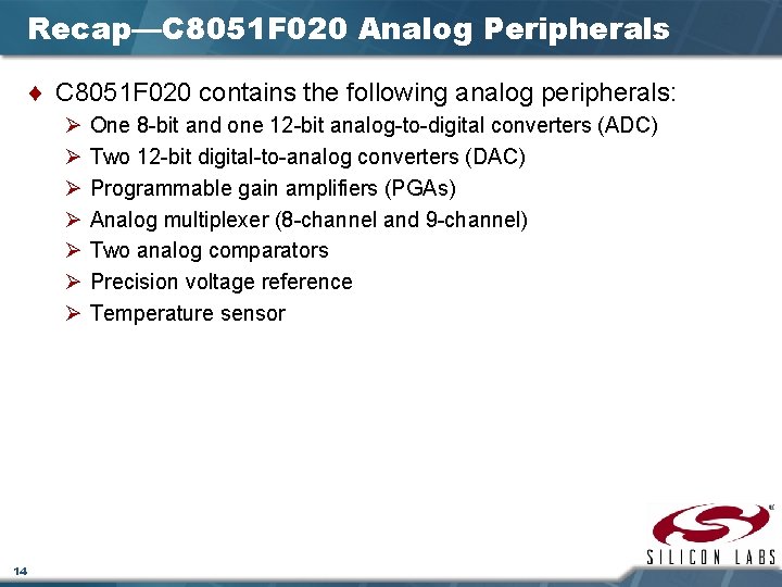
Recap—C 8051 F 020 Analog Peripherals ¨ C 8051 F 020 contains the following analog peripherals: Ø Ø Ø Ø 14 One 8 -bit and one 12 -bit analog-to-digital converters (ADC) Two 12 -bit digital-to-analog converters (DAC) Programmable gain amplifiers (PGAs) Analog multiplexer (8 -channel and 9 -channel) Two analog comparators Precision voltage reference Temperature sensor

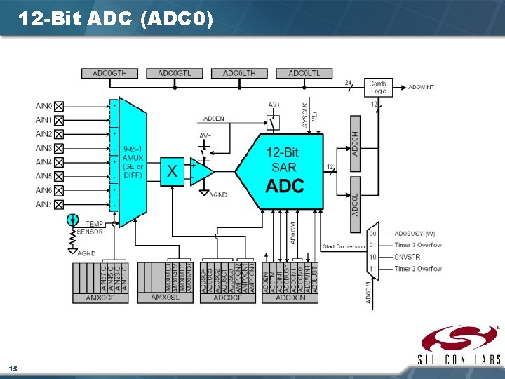
12 -Bit ADC (ADC 0) 15

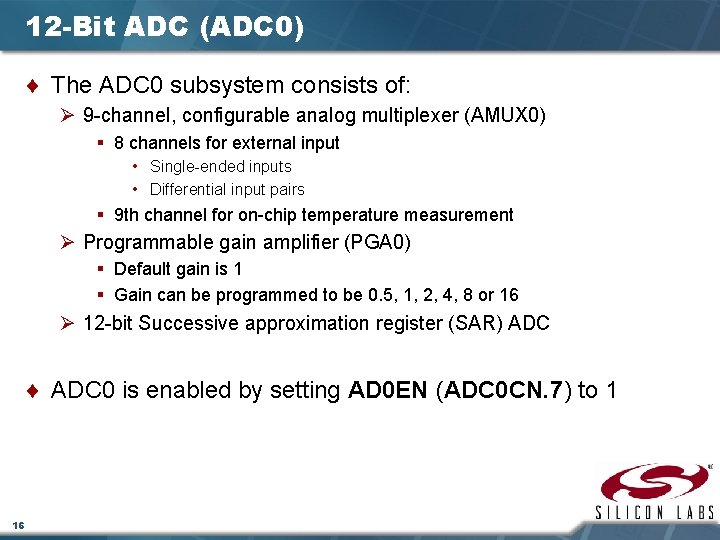
12 -Bit ADC (ADC 0) ¨ The ADC 0 subsystem consists of: Ø 9 -channel, configurable analog multiplexer (AMUX 0) § 8 channels for external input • Single-ended inputs • Differential input pairs § 9 th channel for on-chip temperature measurement Ø Programmable gain amplifier (PGA 0) § Default gain is 1 § Gain can be programmed to be 0. 5, 1, 2, 4, 8 or 16 Ø 12 -bit Successive approximation register (SAR) ADC ¨ ADC 0 is enabled by setting AD 0 EN (ADC 0 CN. 7) to 1 16

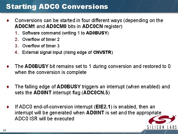
Starting ADC 0 Conversions ¨ Conversions can be started in four different ways (depending on the AD 0 CM 1 and AD 0 CM 0 bits in ADC 0 CN register) 1. 2. 3. 4. Software command (writing 1 to AD 0 BUSY) Overflow of timer 2 Overflow of timer 3 External signal input (rising edge of CNVSTR) ¨ The AD 0 BUSY bit remains set to 1 during conversion and restored to 0 when the conversion is complete ¨ The falling edge of AD 0 BUSY triggers an interrupt (when enabled) and sets the AD 0 INT interrupt flag (ADC 0 CN. 5) ¨ If ADC 0 end-of-conversion interrupt (EIE 2. 1) is enabled, then an interrupt will be generated when AD 0 INT is set and the appropriate ADC 0 ISR will be executed 17

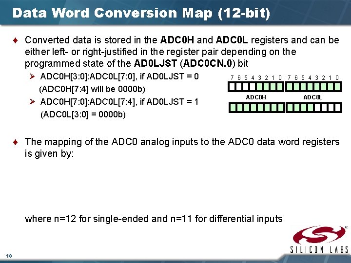
Data Word Conversion Map (12 -bit) ¨ Converted data is stored in the ADC 0 H and ADC 0 L registers and can be either left- or right-justified in the register pair depending on the programmed state of the AD 0 LJST (ADC 0 CN. 0) bit Ø ADC 0 H[3: 0]: ADC 0 L[7: 0], if AD 0 LJST = 0 (ADC 0 H[7: 4] will be 0000 b) Ø ADC 0 H[7: 0]: ADC 0 L[7: 4], if AD 0 LJST = 1 (ADC 0 L[3: 0] = 0000 b) 7 6 5 4 3 2 1 0 ADC 0 H ADC 0 L ¨ The mapping of the ADC 0 analog inputs to the ADC 0 data word registers is given by: where n=12 for single-ended and n=11 for differential inputs 18

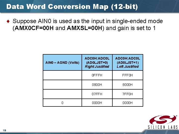
Data Word Conversion Map (12 -bit) ¨ Suppose AIN 0 is used as the input in single-ended mode (AMX 0 CF=00 H and AMXSL=00 H) and gain is set to 1 AIN 0 – AGND (Volts) 0 19 ADC 0 H: ADC 0 L (AD 0 LJST=0) Right Justified ADC 0 H: ADC 0 L (AD 0 LJST=1) Left Justified 0 FFFH FFF 0 H 0800 H 8000 H 07 FFH 7 FF 0 H 0000 H

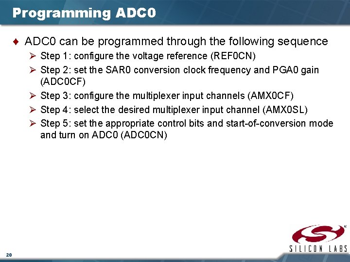
Programming ADC 0 ¨ ADC 0 can be programmed through the following sequence Ø Step 1: configure the voltage reference (REF 0 CN) Ø Step 2: set the SAR 0 conversion clock frequency and PGA 0 gain (ADC 0 CF) Ø Step 3: configure the multiplexer input channels (AMX 0 CF) Ø Step 4: select the desired multiplexer input channel (AMX 0 SL) Ø Step 5: set the appropriate control bits and start-of-conversion mode and turn on ADC 0 (ADC 0 CN) 20

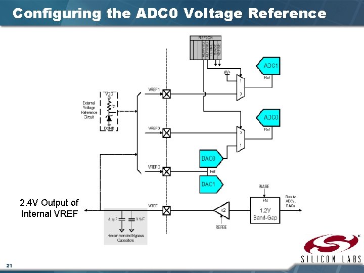
Configuring the ADC 0 Voltage Reference 2. 4 V Output of Internal VREF 21

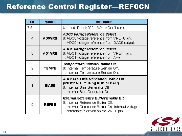
Reference Control Register—REF 0 CN Bit 7 -5 4 3 2 1 0 22 Symbol - Description Unused. Read=000 b; Write=Don’t care. AD 0 VRS ADC 0 Voltage Reference Select 0: ADC 0 voltage reference from VREF 0 pin. 1: ADC 0 voltage reference from DAC 0 output. AD 1 VRS ADC 1 Voltage Reference Select 0: ADC 1 voltage reference from VREF 1 pin. 1: ADC 1 voltage reference from AV+ TEMPE Temperature Sensor Enable Bit 0: Internal Temperature Sensor Off. 1: Internal Temperature Sensor On. BIASE ADC/DAC Bias Generator Enable Bit. (Must be ‘ 1’ if using ADC or DAC) 0: Internal Bias Generator Off. 1: Internal Bias Generator On. REFBE Internal Reference Buffer Enable Bit. 0: Internal Reference Buffer Off. 1: Internal Reference Buffer On. Internal voltage reference is driven on the VREF pin.

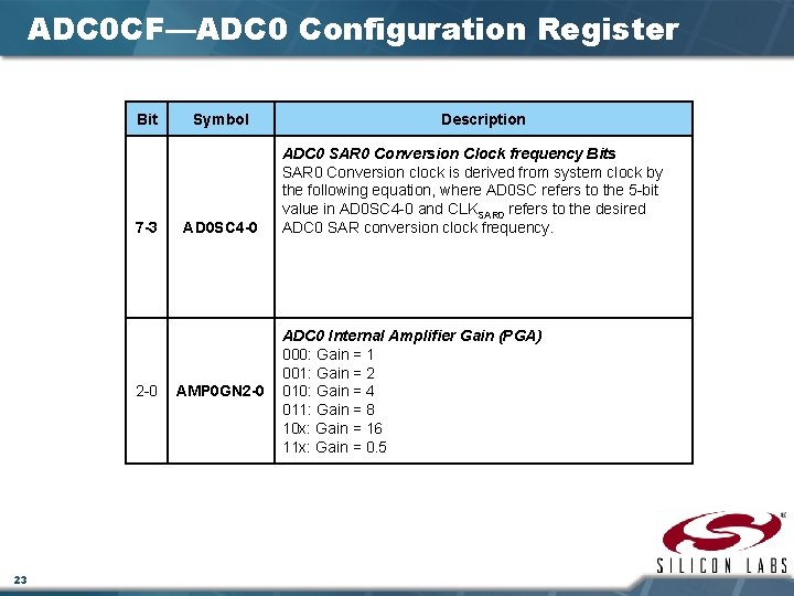
ADC 0 CF—ADC 0 Configuration Register Bit 7 -3 2 -0 23 Symbol AD 0 SC 4 -0 AMP 0 GN 2 -0 Description ADC 0 SAR 0 Conversion Clock frequency Bits SAR 0 Conversion clock is derived from system clock by the following equation, where AD 0 SC refers to the 5 -bit value in AD 0 SC 4 -0 and CLKSAR 0 refers to the desired ADC 0 SAR conversion clock frequency. ADC 0 Internal Amplifier Gain (PGA) 000: Gain = 1 001: Gain = 2 010: Gain = 4 011: Gain = 8 10 x: Gain = 16 11 x: Gain = 0. 5

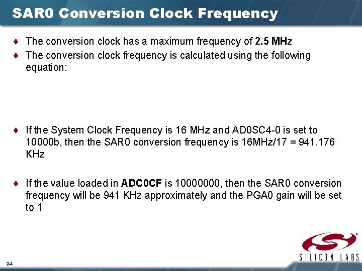
SAR 0 Conversion Clock Frequency ¨ The conversion clock has a maximum frequency of 2. 5 MHz ¨ The conversion clock frequency is calculated using the following equation: ¨ If the System Clock Frequency is 16 MHz and AD 0 SC 4 -0 is set to 10000 b, then the SAR 0 conversion frequency is 16 MHz/17 = 941. 176 KHz ¨ If the value loaded in ADC 0 CF is 10000000, then the SAR 0 conversion frequency will be 941 KHz approximately and the PGA 0 gain will be set to 1 24

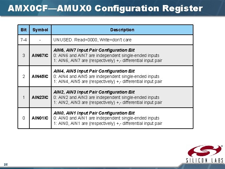
AMX 0 CF—AMUX 0 Configuration Register Bit Symbol 7 -4 - 3 2 1 0 25 Description UNUSED. Read=0000, Write=don’t care AIN 67 IC AIN 6, AIN 7 Input Pair Configuration Bit 0: AIN 6 and AIN 7 are independent single-ended inputs 1: AIN 6, AIN 7 are (respectively) +, - differential input pair AIN 45 IC AIN 4, AIN 5 Input Pair Configuration Bit 0: AIN 4 and AIN 5 are independent single-ended inputs 1: AIN 4, AIN 5 are (respectively) +, - differential input pair AIN 23 IC AIN 2, AIN 3 Input Pair Configuration Bit 0: AIN 2 and AIN 3 are independent single-ended inputs 1: AIN 2, AIN 3 are (respectively) +, - differential input pair AIN 01 IC AIN 0, AIN 1 Input Pair Configuration Bit 0: AIN 0 and AIN 1 are independent single-ended inputs 1: AIN 0, AIN 1 are (respectively) +, - differential input pair

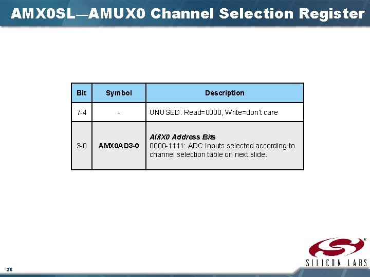
AMX 0 SL—AMUX 0 Channel Selection Register Bit Symbol 7 -4 - 3 -0 26 AMX 0 AD 3 -0 Description UNUSED. Read=0000, Write=don’t care AMX 0 Address Bits 0000 -1111: ADC Inputs selected according to channel selection table on next slide.

AMUX 0 Channel Selection—AMX 0 SL SFR 27

ADC 0 CN—ADC 0 Control Register 28

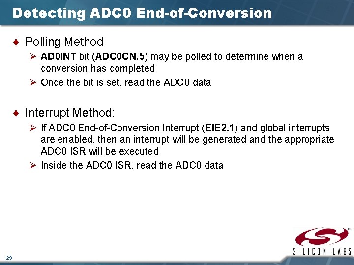
Detecting ADC 0 End-of-Conversion ¨ Polling Method Ø AD 0 INT bit (ADC 0 CN. 5) may be polled to determine when a conversion has completed Ø Once the bit is set, read the ADC 0 data ¨ Interrupt Method: Ø If ADC 0 End-of-Conversion Interrupt (EIE 2. 1) and global interrupts are enabled, then an interrupt will be generated and the appropriate ADC 0 ISR will be executed Ø Inside the ADC 0 ISR, read the ADC 0 data 29

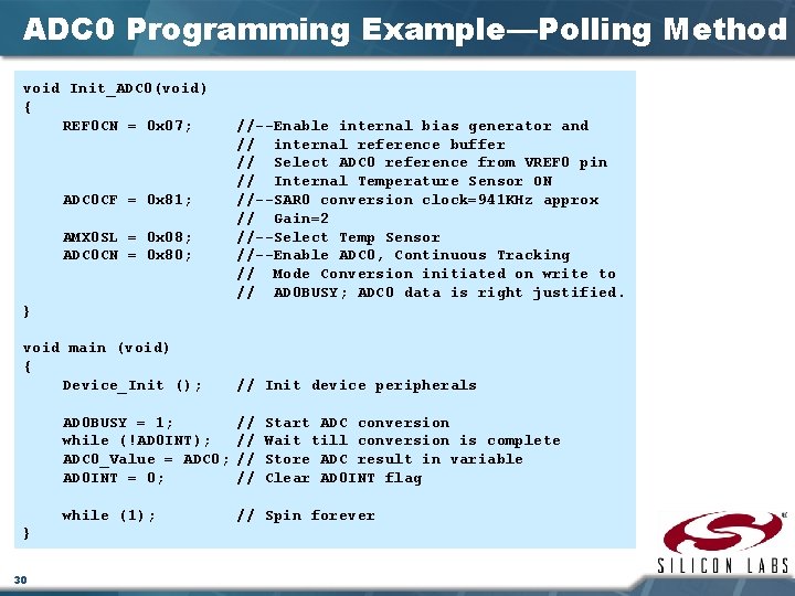
ADC 0 Programming Example—Polling Method void Init_ADC 0(void) { REF 0 CN = 0 x 07; ADC 0 CF = 0 x 81; AMX 0 SL = 0 x 08; ADC 0 CN = 0 x 80; //--Enable internal bias generator and // internal reference buffer // Select ADC 0 reference from VREF 0 pin // Internal Temperature Sensor ON //--SAR 0 conversion clock=941 KHz approx // Gain=2 //--Select Temp Sensor //--Enable ADC 0, Continuous Tracking // Mode Conversion initiated on write to // AD 0 BUSY; ADC 0 data is right justified. } void main (void) { Device_Init (); } 30 // Init device peripherals AD 0 BUSY = 1; while (!AD 0 INT); ADC 0_Value = ADC 0; AD 0 INT = 0; // // Start ADC conversion Wait till conversion is complete Store ADC result in variable Clear AD 0 INT flag while (1); // Spin forever

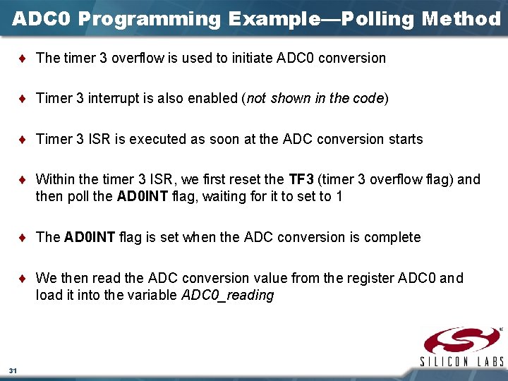
ADC 0 Programming Example—Polling Method ¨ The timer 3 overflow is used to initiate ADC 0 conversion ¨ Timer 3 interrupt is also enabled (not shown in the code) ¨ Timer 3 ISR is executed as soon at the ADC conversion starts ¨ Within the timer 3 ISR, we first reset the TF 3 (timer 3 overflow flag) and then poll the AD 0 INT flag, waiting for it to set to 1 ¨ The AD 0 INT flag is set when the ADC conversion is complete ¨ We then read the ADC conversion value from the register ADC 0 and load it into the variable ADC 0_reading 31

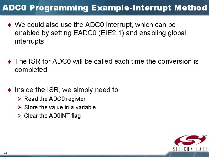
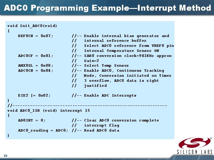
ADC 0 Programming Example-Interrupt Method ¨ We could also use the ADC 0 interrupt, which can be enabled by setting EADC 0 (EIE 2. 1) and enabling global interrupts ¨ The ISR for ADC 0 will be called each time the conversion is completed ¨ Inside the ISR, we simply need to: Ø Read the ADC 0 register Ø Store the value in a variable Ø Clear the AD 0 INT flag 32

ADC 0 Programming Example—Interrupt Method void Init_ADC 0(void) { REF 0 CN = 0 x 07; ADC 0 CF = 0 x 81; AMX 0 SL = 0 x 08; ADC 0 CN = 0 x 84; EIE 2 |= 0 x 02; //-// //-//-// // // Enable internal bias generator and internal reference buffer Select ADC 0 reference from VREF 0 pin Internal Temperature Sensor ON SAR 0 conversion clock=941 KHz approx Gain=2 Select Temp Sensor Enable ADC 0, Continuous Tracking Mode, Conversion initiated on Timer 3 overflow, ADC 0 data is right justified //-- Enable ADC Interrupts } //-------------------------------void ADC 0_ISR (void) interrupt 15 { AD 0 INT = 0; //-- Clear ADC 0 conversion complete // interrupt flag ADC 0_reading = ADC 0; //-- Read ADC 0 data } 33

Appendix

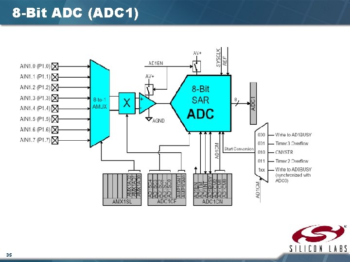
8 -Bit ADC (ADC 1) 35

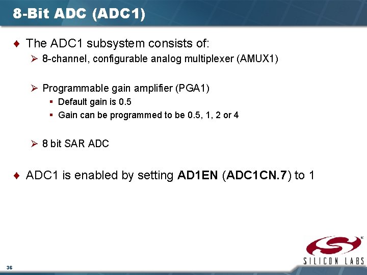
8 -Bit ADC (ADC 1) ¨ The ADC 1 subsystem consists of: Ø 8 -channel, configurable analog multiplexer (AMUX 1) Ø Programmable gain amplifier (PGA 1) § Default gain is 0. 5 § Gain can be programmed to be 0. 5, 1, 2 or 4 Ø 8 bit SAR ADC ¨ ADC 1 is enabled by setting AD 1 EN (ADC 1 CN. 7) to 1 36

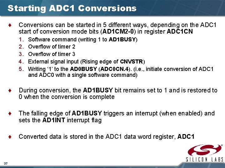
Starting ADC 1 Conversions ¨ Conversions can be started in 5 different ways, depending on the ADC 1 start of conversion mode bits (AD 1 CM 2 -0) in register ADC 1 CN 1. 2. 3. 4. 5. Software command (writing 1 to AD 1 BUSY) Overflow of timer 2 Overflow of timer 3 External signal input (Rising edge of CNVSTR) Writing ‘ 1’ to the AD 0 BUSY (ADC 0 CN. 4). (i. e. , initiate conversion of ADC 1 and ADC 0 with a single software command) ¨ During conversion, the AD 1 BUSY bit remains set to 1 and is restored to 0 when the conversion is complete ¨ The falling edge of AD 1 BUSY triggers an interrupt (when enabled) and sets the AD 1 INT interrupt flag ¨ Converted data is stored in the ADC 1 data word register, ADC 1 37

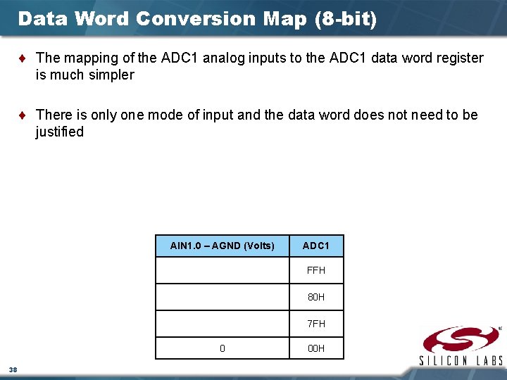
Data Word Conversion Map (8 -bit) ¨ The mapping of the ADC 1 analog inputs to the ADC 1 data word register is much simpler ¨ There is only one mode of input and the data word does not need to be justified AIN 1. 0 – AGND (Volts) ADC 1 FFH 80 H 7 FH 0 38 00 H

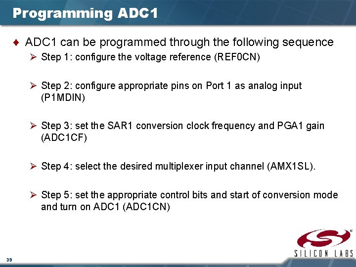
Programming ADC 1 ¨ ADC 1 can be programmed through the following sequence Ø Step 1: configure the voltage reference (REF 0 CN) Ø Step 2: configure appropriate pins on Port 1 as analog input (P 1 MDIN) Ø Step 3: set the SAR 1 conversion clock frequency and PGA 1 gain (ADC 1 CF) Ø Step 4: select the desired multiplexer input channel (AMX 1 SL). Ø Step 5: set the appropriate control bits and start of conversion mode and turn on ADC 1 (ADC 1 CN) 39

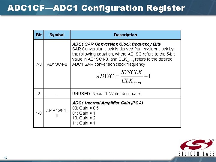
ADC 1 CF—ADC 1 Configuration Register Bit 7 -3 AD 1 SC 4 -0 2 - 1 -0 40 Symbol AMP 1 GN 10 Description ADC 1 SAR Conversion Clock frequency Bits SAR Conversion clock is derived from system clock by the following equation, where AD 1 SC refers to the 5 -bit value in AD 1 SC 4 -0, and CLKSAR 1 refers to the desired ADC 1 SAR conversion clock frequency. UNUSED. Read=0, Write=don’t care ADC 1 Internal Amplifier Gain (PGA) 00: Gain = 0. 5 01: Gain = 1 10: Gain = 2 11: Gain = 4

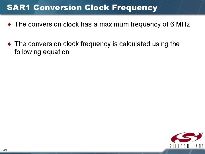
SAR 1 Conversion Clock Frequency ¨ The conversion clock has a maximum frequency of 6 MHz ¨ The conversion clock frequency is calculated using the following equation: 41

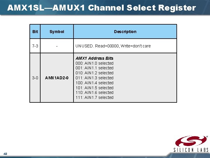
AMX 1 SL—AMUX 1 Channel Select Register Bit Symbol 7 -3 - 3 -0 42 AMX 1 AD 2 -0 Description UNUSED. Read=00000, Write=don’t care AMX 1 Address Bits 000: AIN 1. 0 selected 001: AIN 1. 1 selected 010: AIN 1. 2 selected 011: AIN 1. 3 selected 100: AIN 1. 4 selected 101: AIN 1. 5 selected 110: AIN 1. 6 selected 111: AIN 1. 7 selected

ADC 1 CN—ADC 1 Control Register 43

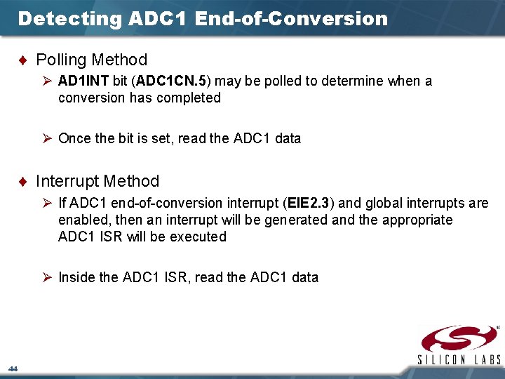
Detecting ADC 1 End-of-Conversion ¨ Polling Method Ø AD 1 INT bit (ADC 1 CN. 5) may be polled to determine when a conversion has completed Ø Once the bit is set, read the ADC 1 data ¨ Interrupt Method Ø If ADC 1 end-of-conversion interrupt (EIE 2. 3) and global interrupts are enabled, then an interrupt will be generated and the appropriate ADC 1 ISR will be executed Ø Inside the ADC 1 ISR, read the ADC 1 data 44

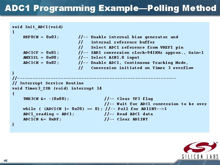
ADC 1 Programming Example—Polling Method void Init_ADC 1(void) { REF 0 CN = 0 x 03; ADC 1 CF = 0 x 81; AMX 1 SL = 0 x 00; ADC 1 CN = 0 x 82; //-// // //-//-//-// Enable internal bias generator and internal reference buffer Select ADC 1 reference from VREF 1 pin SAR 1 conversion clock=941 KHz approx. , Gain=1 Select AIN 1. 0 input Enable ADC 1, Continuous Tracking Mode, Conversion initiated on Timer 3 overflow } //-------------------------------// Interrupt Service Routine void Timer 3_ISR (void) interrupt 14 { TMR 3 CN &= ~(0 x 80); //-- Clear TF 3 flag //-- Wait for ADC 1 conversion to be over while ( (ADC 1 CN |= 0 x 20) == 0); //-- Poll for AD 1 INT-->1 ADC 1_reading = ADC 1; //-- Read ADC 1 data ADC 1 CN &= 0 x. DF; //-- Clear AD 1 INT } 45

ADC 1 Programming—Interrupt Method ¨ Instead of using the polling technique as illustrated in the code on the previous slide, we could also use interrupt method ¨ The ADC 1 interrupt can be enabled by setting EADC 1 (EIE 2. 3) and enabling global interrupts ¨ The ISR for ADC 1 will be called each time the conversion is completed ¨ Inside the ISR, we simply need to: Ø Read the ADC 1 register Ø Store the value in a variable Ø Clear the AD 1 INT flag 46

www. silabs. com/MCU