Lecture 11 Combinational Design Procedure 1 Overview Design
Lecture 11 Combinational Design Procedure 1
Overview ° Design digital circuit from specification ° Digital inputs and outputs known • Need to determine logic that can transform data ° Start in truth table form ° Create K-map for each output based on function of inputs ° Determine minimized sum-of-product representation ° Draw circuit diagram 2

Design Procedure (Mano) Design a circuit from a specification. 1. Determine number of required inputs and outputs. 2. Derive truth table 3. Obtain simplified Boolean functions 4. Draw logic diagram and verify correctness A B C RS 0 0 0 0 1 0 1 0 0 1 S=A+B+C R = ABC 0 1 1 0 0 0 1 1 1 0 0 1 1 1 3

Previously, we have learned… ° Boolean algebra can be used to simplify expressions, but not obvious: • how to proceed at each step, or • if solution reached is minimal. ° Have seen five ways to represent a function: • • • Boolean expression truth table logic circuit minterms/maxterms Karnaugh map 4
Combinational logic design ° Use multiple representations of logic functions ° Use graphical representation to assist in simplification of function. ° Use concept of “don’t care” conditions. ° Example - encoding BCD to seven segment display. ° Similar to approach used by designers in the field. 5

BCD to Seven Segment Display ° Used to display binary coded decimal (BCD) numbers using seven illuminated segments. ° BCD uses 0’s and 1’s to represent decimal digits 0 9. Need four bits to represent required 10 digits. ° Binary coded decimal (BCD) represents each decimal digit with four bits a f g e b c d 6
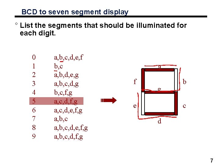
BCD to seven segment display ° List the segments that should be illuminated for each digit. 0 1 2 3 4 5 6 7 8 9 a, b, c, d, e, f b, c a, b, d, e, g a, b, c, d, g b, c, f, g a, c, d, e, f, g a, b, c, d, f, g a f g e b c d 7
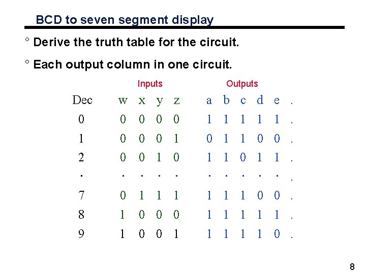
BCD to seven segment display ° Derive the truth table for the circuit. ° Each output column in one circuit. Inputs Outputs Dec w x y z a b c d e. 0 0 0 1 1 1. 1 0 0 0 1 1 0 0. 2 × 0 0 1 0 × × 1 1 0 1 1. × × ×. 7 0 1 1 1 0 0. 8 1 0 0 0 1 1 1. 9 1 0 0 1 1 1 0. 8
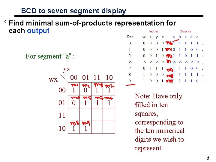
BCD to seven segment display ° Find minimal sum-of-products representation for each output For segment “a” : yz 00 01 11 10 wx 00 1 1 01 0 1 11 10 1 1 Note: Have only filled in ten squares, corresponding to the ten numerical digits we wish to represent. 9

Don’t care conditions (BCD display). . . ° Fill in don’t cares for undefined outputs. • Note that these combinations of inputs should never happen. ° Leads to a reduced implementation For segment “a” : yz 00 01 11 10 wx 00 1 1 01 0 1 11 X X 10 1 1 Put in “X” (don’t care), and interpret as either 1 or 0 as desired …. X X 10

Don’t care conditions (BCD display). . . ° Circle biggest group of 1’s and Don’t Cares. ° Leads to a reduced implementation For segment “a” : yz 00 01 11 10 wx 00 1 1 01 0 1 11 X X 10 1 1 X X 11
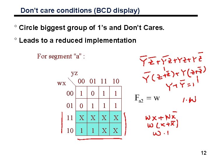
Don’t care conditions (BCD display) ° Circle biggest group of 1’s and Don’t Cares. ° Leads to a reduced implementation For segment “a” : yz wx 00 01 11 10 00 1 1 01 0 1 11 X X 10 1 1 X X 12
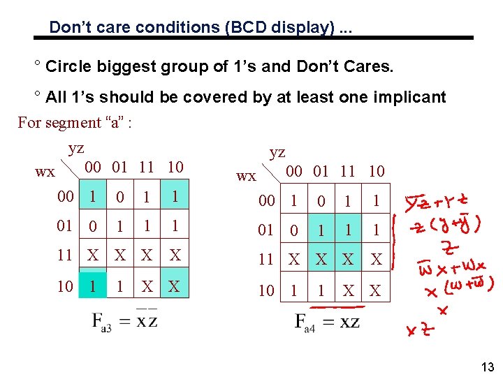
Don’t care conditions (BCD display). . . ° Circle biggest group of 1’s and Don’t Cares. ° All 1’s should be covered by at least one implicant For segment “a” : yz yz 00 01 11 10 wx 00 1 0 1 1 01 0 1 1 1 11 X X X X 10 1 1 X X 13
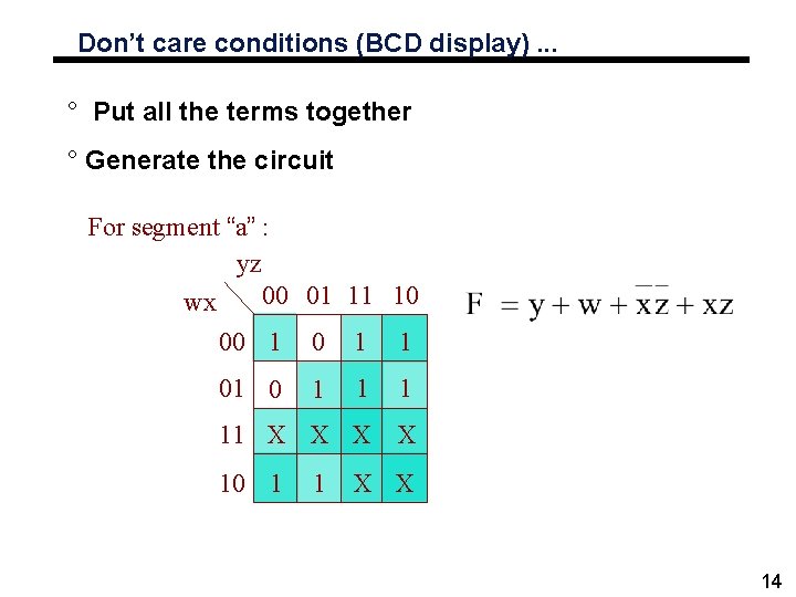
Don’t care conditions (BCD display). . . ° Put all the terms together ° Generate the circuit For segment “a” : yz 00 01 11 10 wx 00 1 1 01 0 1 11 X X 10 1 1 X X 14
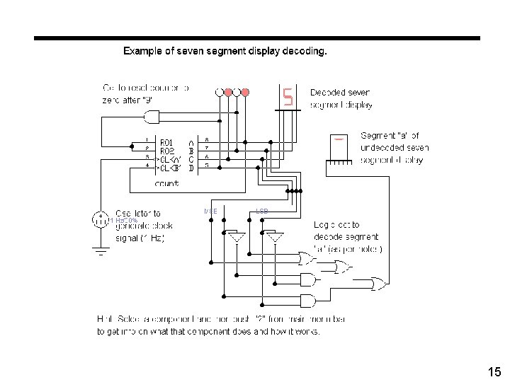
15

BCD to seven segment display ° Derive the truth table for the circuit. ° Each output column in one circuit. Inputs Outputs Dec w x y z a b c d e. 0 0 0 1 1 1. 1 0 0 0 1 1 0 0. 2 × 0 0 1 0 × × 1 1 0 1 1. × × ×. 7 0 1 1 1 0 0. 8 1 0 0 0 1 1 1. 9 1 0 0 1 1 1 0. 16
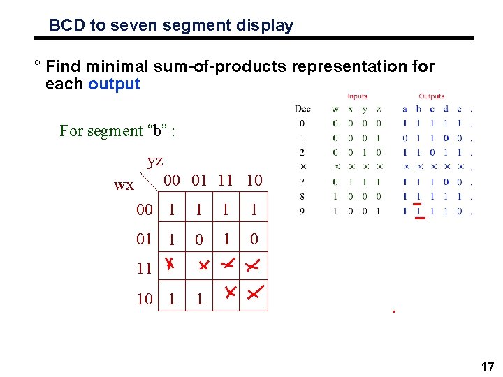
BCD to seven segment display ° Find minimal sum-of-products representation for each output For segment “b” : yz 00 01 11 10 wx 00 1 1 01 1 0 11 10 1 1 17
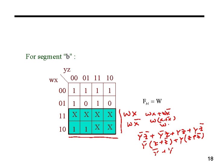
For segment “b” : yz wx 00 01 11 10 00 1 1 01 1 0 11 X X 10 1 18
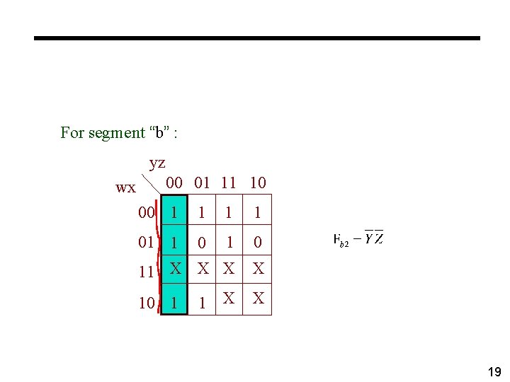
For segment “b” : yz wx 00 01 11 10 00 1 1 01 1 0 11 X X 10 1 19
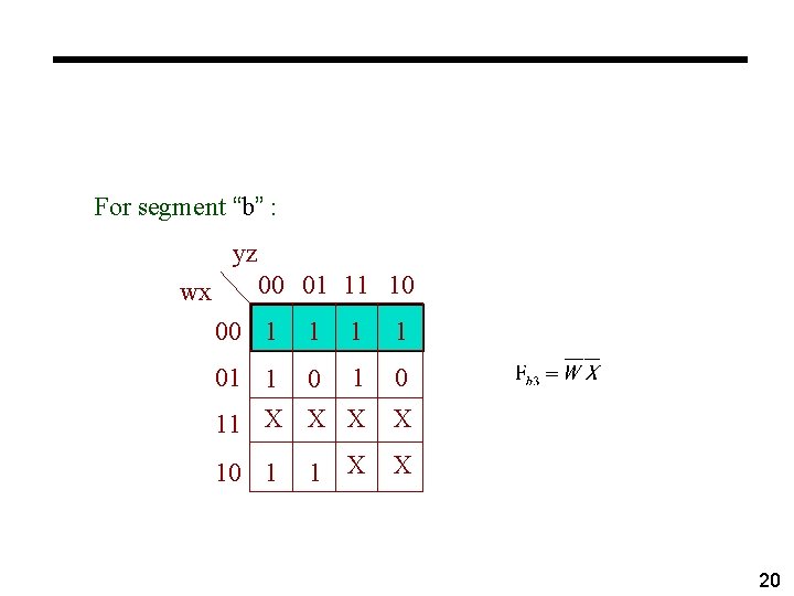
For segment “b” : yz wx 00 01 11 10 00 1 1 01 1 0 11 X X 10 1 20
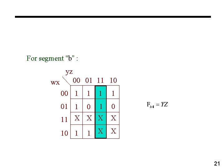
For segment “b” : yz wx 00 01 11 10 00 1 1 01 1 0 11 X X 10 1 21
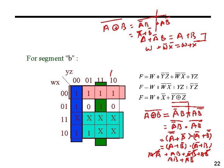
For segment “b” : yz wx 00 01 11 10 00 1 1 01 1 0 11 X X 10 1 22
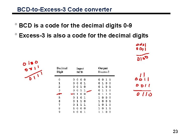
BCD-to-Excess-3 Code converter ° BCD is a code for the decimal digits 0 -9 ° Excess-3 is also a code for the decimal digits 23
Specification of BCD-to-Excess 3 ° Inputs: a BCD input, A, B, C, D with A as the most significant bit and D as the least significant bit. ° Outputs: an Excess-3 output W, X, Y, Z that corresponds to the BCD input. ° Internal operation – circuit to do the conversion in combinational logic. 24

Formulation of BCD-to-Excess-3 ° Excess-3 code is easily formed by adding a binary 3 to the binary or BCD for the digit. ° There are 16 possible inputs for both BCD and Excess-3. ° It can be assumed that only valid BCD inputs will appear so the six combinations not used can be treated as don’t cares. 25
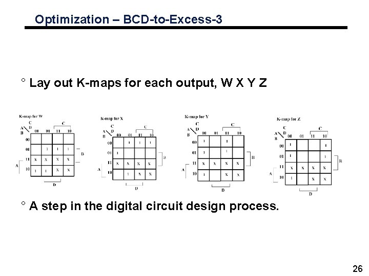
Optimization – BCD-to-Excess-3 ° Lay out K-maps for each output, W X Y Z ° A step in the digital circuit design process. 26
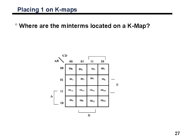
Placing 1 on K-maps ° Where are the minterms located on a K-Map? 27
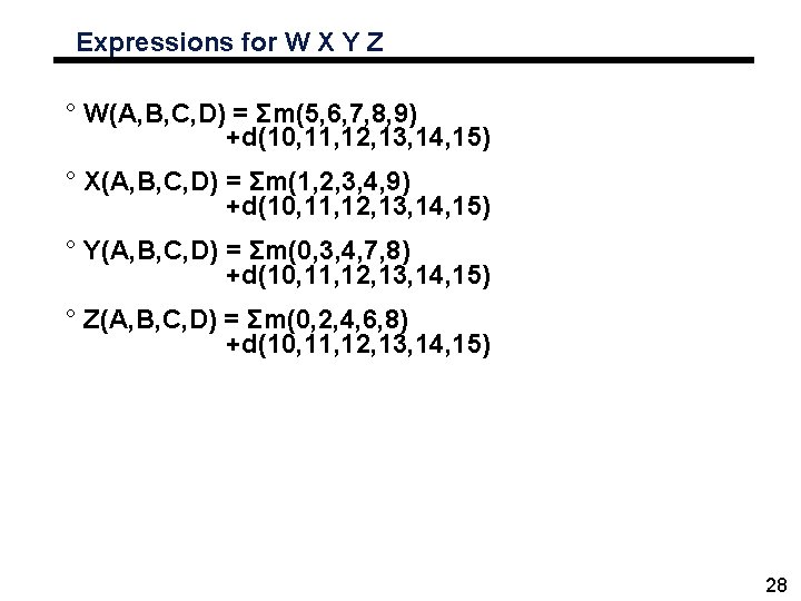
Expressions for W X Y Z ° W(A, B, C, D) = Σm(5, 6, 7, 8, 9) +d(10, 11, 12, 13, 14, 15) ° X(A, B, C, D) = Σm(1, 2, 3, 4, 9) +d(10, 11, 12, 13, 14, 15) ° Y(A, B, C, D) = Σm(0, 3, 4, 7, 8) +d(10, 11, 12, 13, 14, 15) ° Z(A, B, C, D) = Σm(0, 2, 4, 6, 8) +d(10, 11, 12, 13, 14, 15) 28
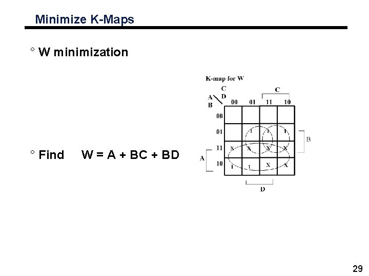
Minimize K-Maps ° W minimization ° Find W = A + BC + BD 29
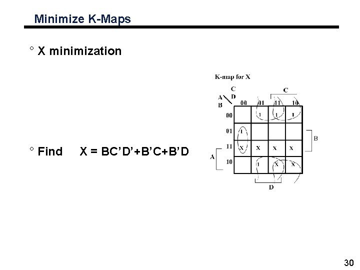
Minimize K-Maps ° X minimization ° Find X = BC’D’+B’C+B’D 30
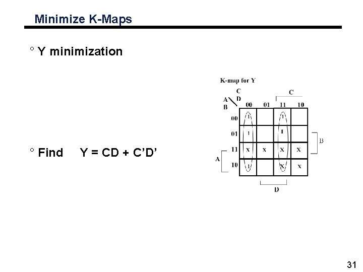
Minimize K-Maps ° Y minimization ° Find Y = CD + C’D’ 31
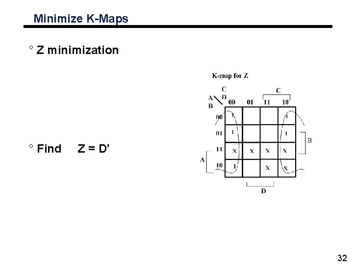
Minimize K-Maps ° Z minimization ° Find Z = D’ 32
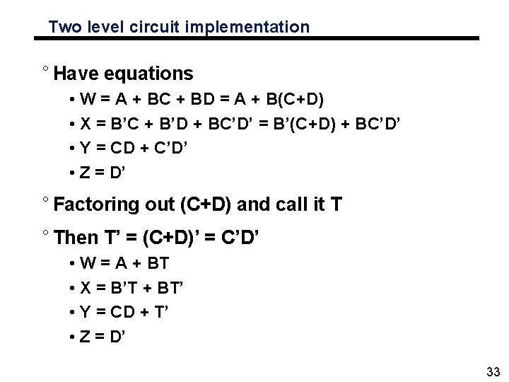
Two level circuit implementation ° Have equations • W = A + BC + BD = A + B(C+D) • X = B’C + B’D + BC’D’ = B’(C+D) + BC’D’ • Y = CD + C’D’ • Z = D’ ° Factoring out (C+D) and call it T ° Then T’ = (C+D)’ = C’D’ • W = A + BT • X = B’T + BT’ • Y = CD + T’ • Z = D’ 33
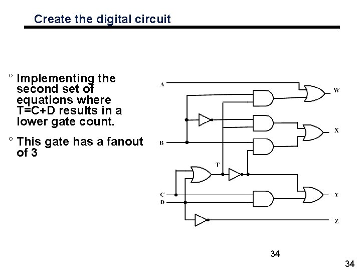
Create the digital circuit ° Implementing the second set of equations where T=C+D results in a lower gate count. ° This gate has a fanout of 3 34 34
Summary ° Need to formulate circuits from problem descriptions 1. 2. 3. 4. Determine number of inputs and outputs Determine truth table format Determine K-map Determine minimal SOP o There may be multiple outputs per design o Solve each output separately o Current approach doesn’t have memory. o This will be covered next week. 35
- Slides: 35