Lecture 10 MetalOxideSemiconductor MOS FieldEffect Transistors FET MOSFET
 Field-Effect Transistors (FET) MOSFET Bias Analysis")

 • Use")


 Also But VDS<VGS-VTN. Hence, saturation region assumption")

 Assumption: Transistor is saturated, IG=IB=0 Analysis: First, simplify")
 (contd. ) Since VGS<VTN for VGS= -2. 71")

 Since VGS<VTN for VGS= -0. 769 V and")

 For Q 1 For Q 2")
1 (W/L)2 In W/L (W/L)n")


 Also Since VGS= -0. 369")
 = 2 m.")


 i. D Variations in K’(W/L) VG Rs")
- Slides: 25
Lecture 10 Metal-Oxide-Semiconductor (MOS) Field-Effect Transistors (FET) MOSFET Bias Analysis
Goals • Investigate circuits that bias transistors into different operating regions. • • Two Supplies Biasing Four Resistor Biasing Two Resistor Biasing using Current Mirror • Understand Bias Point Stability • Investigate DC Analysis for P-Channel Transistor
Bias Analysis Approach • Assume an operation region (generally the saturation region) • Use circuit analysis to find VGS • Use VGS to calculate ID, and ID to find VDS • Check validity of operation region assumptions • Change assumptions and analyze again if required. NOTE : An enhancement-mode device with VDS = VGS is always in saturation
Bias Analysis of n-channel MOSFET we start the analysis by assuming certain operating region VGS< VTN Cutoff region i. D=0 Check VGS> Vt VDS < VGS –VTN Triode region VDS > VGS –VTN Sat. region
Example-1 Biasing using two voltage supplies for gate and drain terminal
Example 2 ( Biasing in Triode Region) Also But VDS<VGS-VTN. Hence, saturation region assumption is incorrect Using triode region equation, Assumption: IG=IB=0, transistor is saturated (since VDS= VGS) Analysis: VGS=VDD=4 V and ID=1. 06 m. A VDS<VGS-VTN, transistor is in triode region Q-pt: (1. 06 m. A, 2. 3 V)
Four-Resistor and Two-Resistor Biasing • Provide excellent bias for transistors in discrete circuits. • Stabilize bias point with respect to device parameter and temperature variations using negative feedback. • Use single voltage source to supply both gate-bias voltage and drain current. • Generally used to bias transistors in saturation region. • Two-resistor biasing uses lesser components that fourresistor biasing and also isolates drain and gate terminals
Bias Analysis: Example 3 (Four-Resistor Biasing) Assumption: Transistor is saturated, IG=IB=0 Analysis: First, simplify circuit, split VDD into two equal-valued sources and apply Thevenin transformation to find VEQ and REQ for gate-bias voltage Problem: Find Q-pt (ID, VDS) Approach: Assume operation region, find Q-point, check to see if result is consistent with operation region
Bias Analysis: Example 3 (Four-Resistor Biasing) (contd. ) Since VGS<VTN for VGS= -2. 71 V and MOSFET will be cut-off, and ID= 34. 4 m. A Also, Since IG=0, VDS>VGS-VTN. Hence saturation region assumption is correct. Q-pt: (34. 4 m. A, 6. 08 V) with VGS= 2. 66 V
Two Resistor Biasing the MOSFET using a large drain-to-gate feedback resistance, RG. VDD> Vt MOS is ON and always in saturation (diode connected transistor)
Bias Analysis: Example 4 (Two-Resistor Biasing) Since VGS<VTN for VGS= -0. 769 V and MOSFET will be cut-off, Assumption: IG=IB=0, transistor is saturated (since VDS= VGS) Analysis: and ID= 130 m. A VDS>VGS-VTN. Hence saturation region assumption is correct. Q-pt: (130 m. A, 2. 00 V)
Additional Biasing Circuits_2 Using constant current source
How to implement a current source (Current mirrors) For Q 1 For Q 2
N-branch current mirror Iref I 1 I 2 (W/L)1 (W/L)2 In W/L (W/L)n
n-channel and P-Channel MOSFETs
DC –Analysis of P-channel MOS Note: The direction of current is out of the drain for a PMOS
Bias Analysis: Example 5 (Two-Resistor biasing for PMOS Transistor) Also Since VGS= -0. 369 V is less than VTP= -2 V, VGS = -3. 45 V Assumption: IG=IB=0, transistor is saturated (since VDS= VGS) ID = 52. 5 m. A and VGS = -3. 45 V Analysis: Hence saturation assumption is correct. Q-pt: (52. 5 m. A, -3. 45 V)
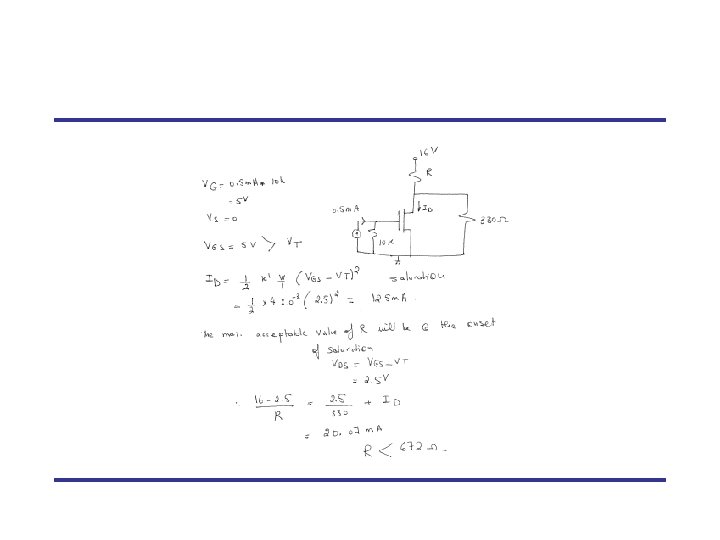
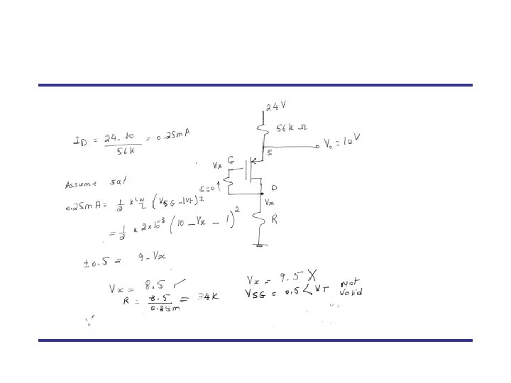
Example The circuit below uses a p-channel enhancement MOSFET with k’(W/L) = 2 m. A/V 2 and Vt = -1 V. Find the value for R that produces V 0 = 10 V.
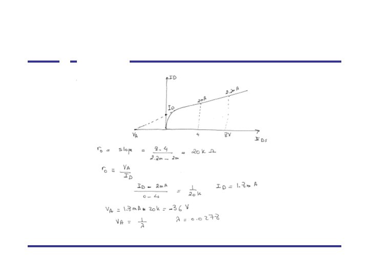
Modifications to Drain Current Equations Channel-Length Modulation Increasing v. DS beyond v. DSsat causes the channel pinch-off point to move slightly away from the drain, thus reducing the effective channel length (by ΔL). Effect of v. DS on i. D in the saturation region. The MOSFET parameter VA depends on the process technology and, for a given process, is proportional to the channel length L. It can be called; channel length modulation (λ), or Early voltage (VA)
Example • A saturated MOSFET is operated with a constant v. GS. The drain current, i. D, is found to be 2 m. A for v. DS = 4 V and 2. 2 m. A for v. DS = 8 V. Find the values of VA, λ and ro.
Including the effect of Channel Length Modulation in the MOSFET model (Valid in the Saturation region) Output resistance
Bias-Point Stability for MOS Amplifiers (source degeneration) i. D Variations in K’(W/L) VG Rs RS Rs VGS=VG-i. DRS Large Rs stable bias point but requires large supply voltage Rs is called degeneration resistance VGS Vt 1 Vt 2 Variation in Vt