Lecture 1 INTRODUCTION TO VERILOG DESIGN 1 The



- Slides: 25

Lecture 1 INTRODUCTION TO VERILOG DESIGN 1

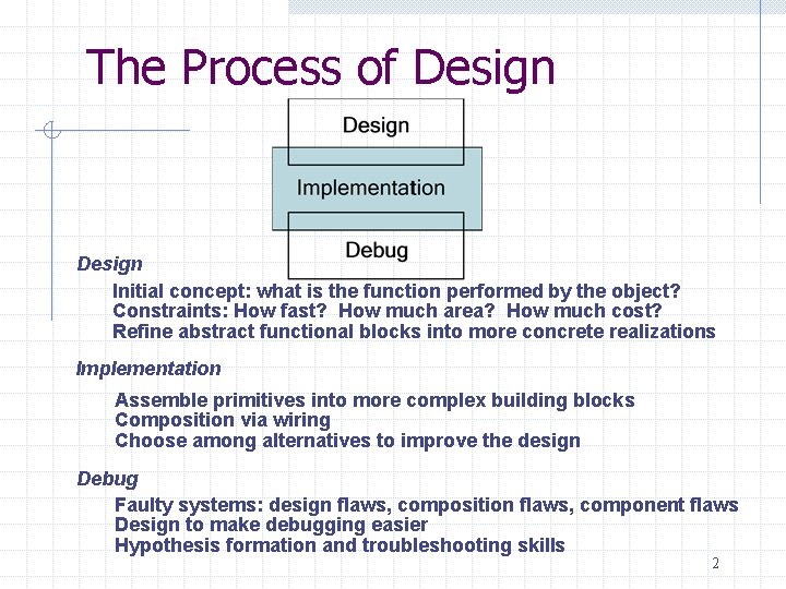
The Process of Design Initial concept: what is the function performed by the object? Constraints: How fast? How much area? How much cost? Refine abstract functional blocks into more concrete realizations Implementation Assemble primitives into more complex building blocks Composition via wiring Choose among alternatives to improve the design Debug Faulty systems: design flaws, composition flaws, component flaws Design to make debugging easier Hypothesis formation and troubleshooting skills 2

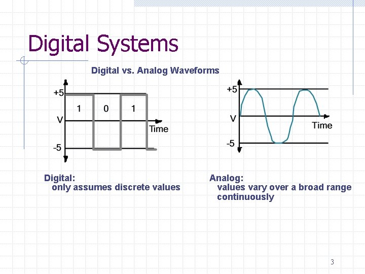
Digital Systems Digital vs. Analog Waveforms Digital: only assumes discrete values Analog: values vary over a broad range continuously 3

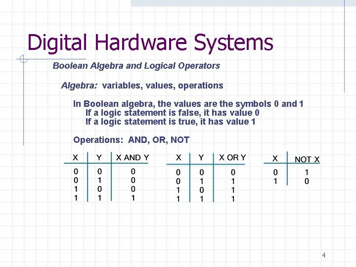
Digital Hardware Systems Boolean Algebra and Logical Operators Algebra: variables, values, operations In Boolean algebra, the values are the symbols 0 and 1 If a logic statement is false, it has value 0 If a logic statement is true, it has value 1 Operations: AND, OR, NOT 4

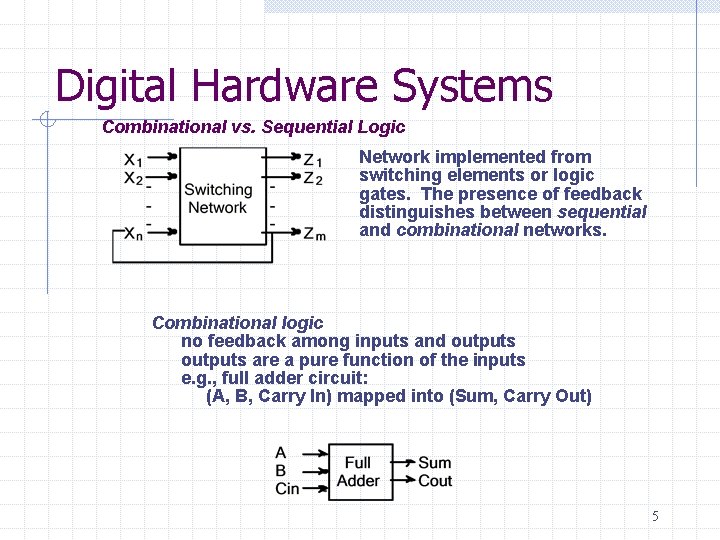
Digital Hardware Systems Combinational vs. Sequential Logic Network implemented from switching elements or logic gates. The presence of feedback distinguishes between sequential and combinational networks. Combinational logic no feedback among inputs and outputs are a pure function of the inputs e. g. , full adder circuit: (A, B, Carry In) mapped into (Sum, Carry Out) 5

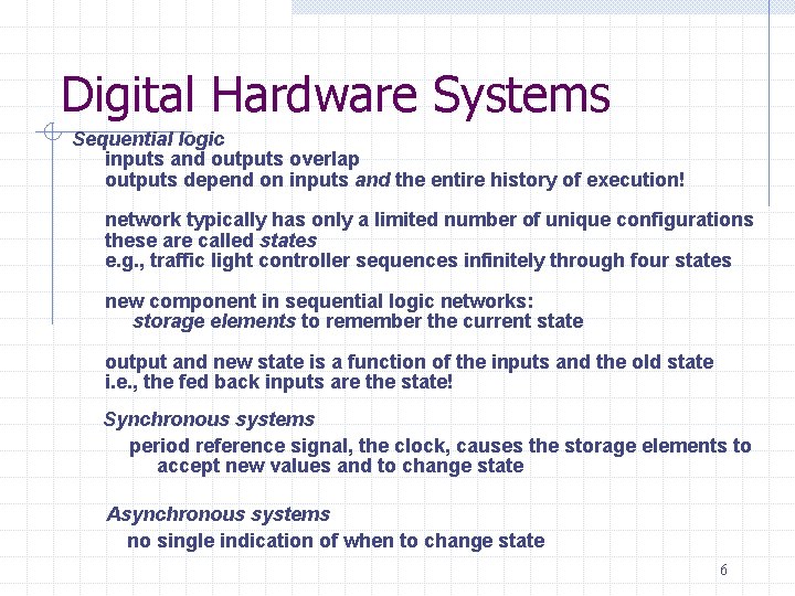
Digital Hardware Systems Sequential logic inputs and outputs overlap outputs depend on inputs and the entire history of execution! network typically has only a limited number of unique configurations these are called states e. g. , traffic light controller sequences infinitely through four states new component in sequential logic networks: storage elements to remember the current state output and new state is a function of the inputs and the old state i. e. , the fed back inputs are the state! Synchronous systems period reference signal, the clock, causes the storage elements to accept new values and to change state Asynchronous systems no single indication of when to change state 6

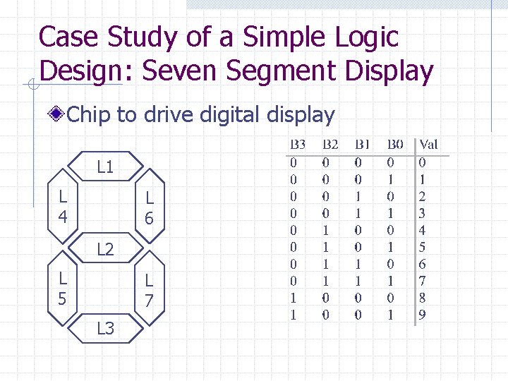
Case Study of a Simple Logic Design: Seven Segment Display Chip to drive digital display L 1 L 4 L 6 L 2 L 5 L 7 L 3

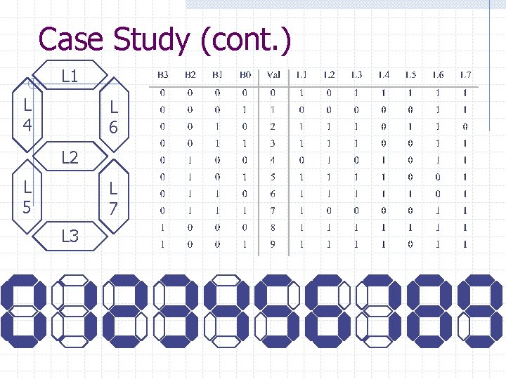
Case Study (cont. ) L 1 L 4 L 6 L 2 L 5 L 7 L 3

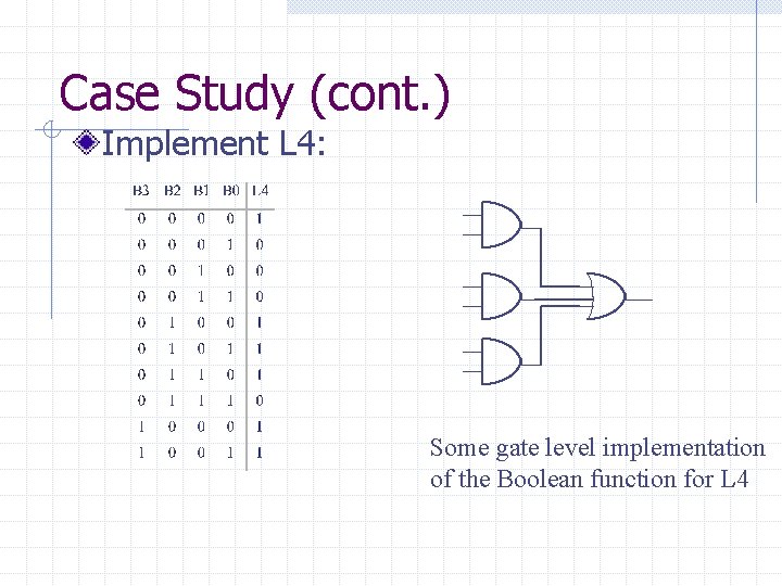
Case Study (cont. ) Implement L 4: Some gate level implementation of the Boolean function for L 4

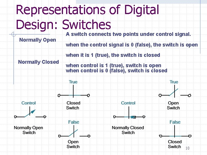
Representations of Digital Design: Switches Normally Open A switch connects two points under control signal. when the control signal is 0 (false), the switch is open when it is 1 (true), the switch is closed Normally Closed when control is 1 (true), switch is open when control is 0 (false), switch is closed 10

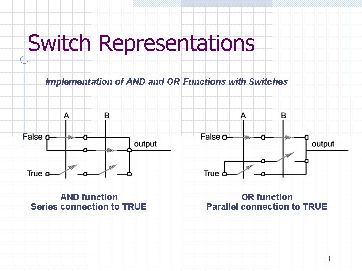
Switch Representations Implementation of AND and OR Functions with Switches AND function Series connection to TRUE OR function Parallel connection to TRUE 11

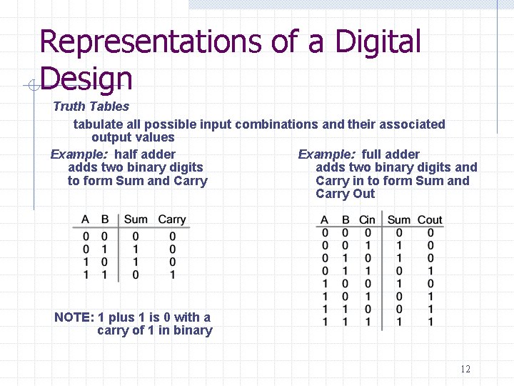
Representations of a Digital Design Truth Tables tabulate all possible input combinations and their associated output values Example: half adder Example: full adder adds two binary digits and to form Sum and Carry in to form Sum and Carry Out NOTE: 1 plus 1 is 0 with a carry of 1 in binary 12

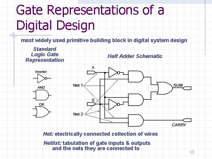
Gate Representations of a Digital Design most widely used primitive building block in digital system design Standard Logic Gate Representation Half Adder Schematic Net: electrically connected collection of wires Netlist: tabulation of gate inputs & outputs and the nets they are connected to 13

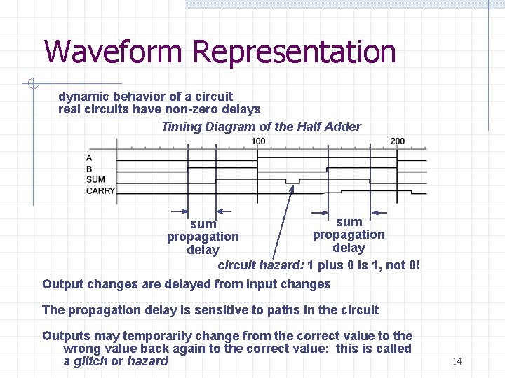
Waveform Representation dynamic behavior of a circuit real circuits have non-zero delays Timing Diagram of the Half Adder sum propagation delay circuit hazard: 1 plus 0 is 1, not 0! Output changes are delayed from input changes The propagation delay is sensitive to paths in the circuit Outputs may temporarily change from the correct value to the wrong value back again to the correct value: this is called a glitch or hazard 14

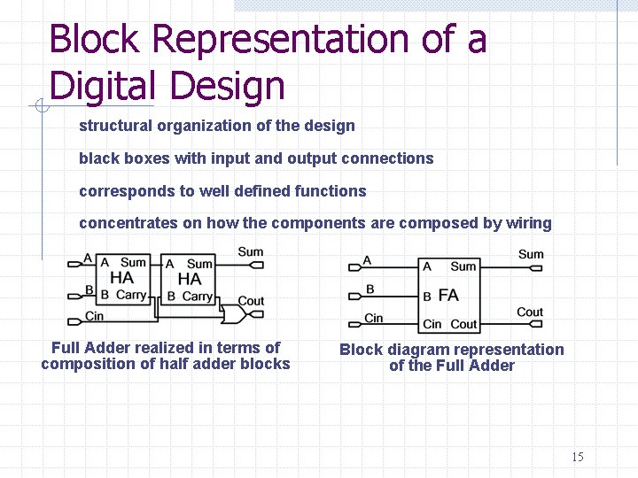
Block Representation of a Digital Design structural organization of the design black boxes with input and output connections corresponds to well defined functions concentrates on how the components are composed by wiring Full Adder realized in terms of composition of half adder blocks Block diagram representation of the Full Adder 15

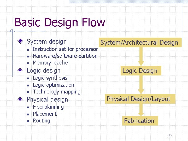
Basic Design Flow System design n Instruction set for processor Hardware/software partition Memory, cache Logic design n System/Architectural Design Logic synthesis Logic optimization Technology mapping Physical design Physical Design/Layout Floorplanning Placement Routing Fabrication n 16

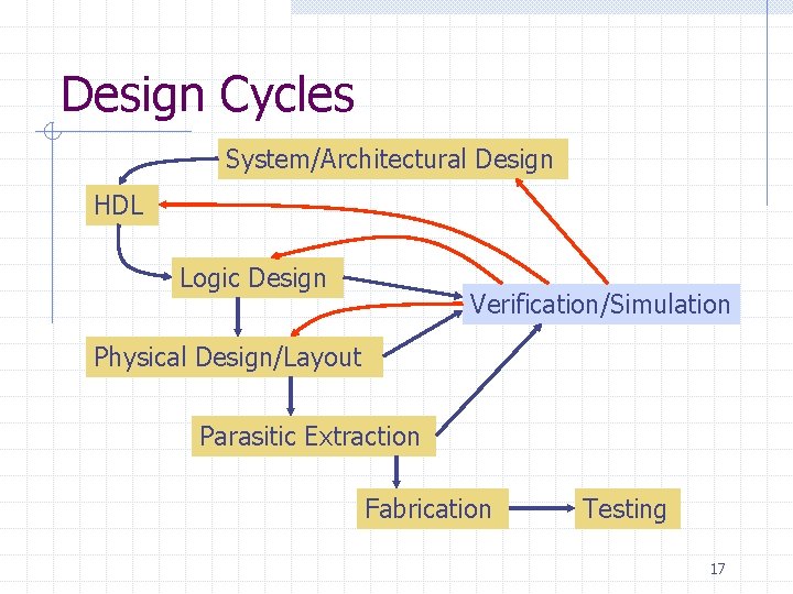
Design Cycles System/Architectural Design HDL Logic Design Verification/Simulation Physical Design/Layout Parasitic Extraction Fabrication Testing 17

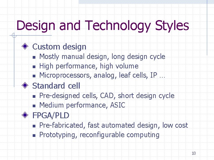
Design and Technology Styles Custom design n Mostly manual design, long design cycle High performance, high volume Microprocessors, analog, leaf cells, IP … Standard cell n n Pre-designed cells, CAD, short design cycle Medium performance, ASIC FPGA/PLD n n Pre-fabricated, fast automated design, low cost Prototyping, reconfigurable computing 18

Why do we need HDLs ? HDL can describe both circuit structure and behavior n n Schematics describe only circuit structure C language describes only behaviors Provide high level abstraction to speed up design High portability and readability Enable rapid prototyping Support different hardware styles 19

What do we need from HDLs ? Describe n n n Combinational logic Level sensitive storage devices Edge-triggered storage devices Provide different levels of abstraction and support hierarchical design n n System level RTL level Gate level Transistor level Physical level Support for hardware concurrency 20

Two major HDLs Verilog n n n Slightly better at gate/transistor level Language style close to C/C++ Pre-defined data type, easy to use VHDL n n n Slightly better at system level Language style close to Pascal User-defined data type, more flexible Equally effective, personal preference 21

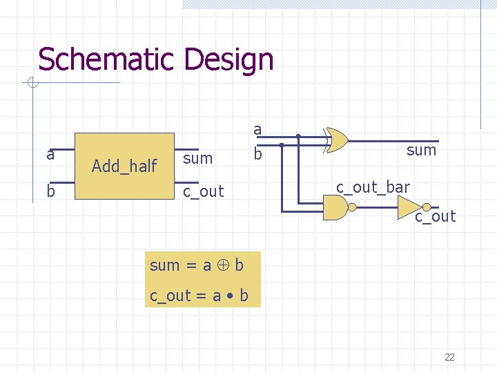
Schematic Design a b Add_half sum c_out a b sum c_out_bar c_out sum = a b c_out = a • b 22

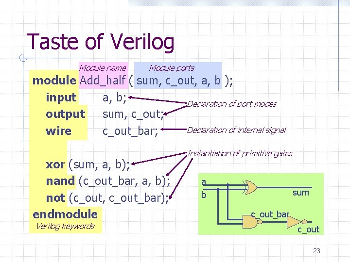
Taste of Verilog Module name Module ports module Add_half ( sum, c_out, a, b ); input a, b; Declaration of port modes output sum, c_out; Declaration of internal signal wire c_out_bar; xor (sum, a, b); nand (c_out_bar, a, b); not (c_out, c_out_bar); endmodule Verilog keywords Instantiation of primitive gates a b sum c_out_bar c_out 23

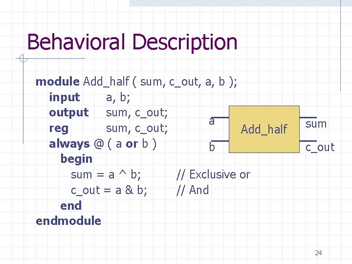
Behavioral Description module Add_half ( sum, c_out, a, b ); input a, b; output sum, c_out; a reg sum, c_out; Add_half always @ ( a or b ) b begin sum = a ^ b; // Exclusive or c_out = a & b; // And endmodule sum c_out 24

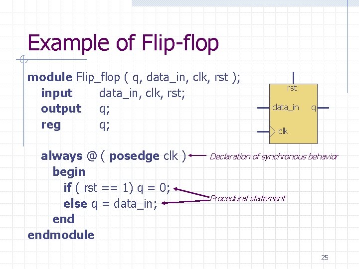
Example of Flip-flop module Flip_flop ( q, data_in, clk, rst ); input data_in, clk, rst; output q; reg q; always @ ( posedge clk ) begin if ( rst == 1) q = 0; else q = data_in; endmodule rst data_in q clk Declaration of synchronous behavior Procedural statement 25