LEC 10 ACTIVE FILTERS PARASITIC OSCILLATIONS Perfect Brickwall
LEC 10 ACTIVE FILTERS & PARASITIC OSCILLATIONS
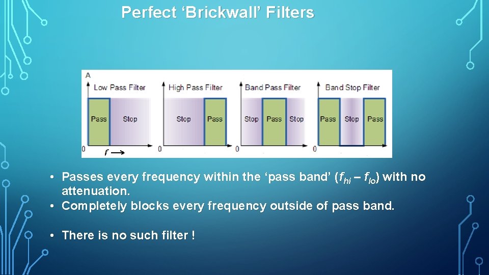
Perfect ‘Brickwall’ Filters • Passes every frequency within the ‘pass band’ (fhi – flo) with no attenuation. • Completely blocks every frequency outside of pass band. • There is no such filter !
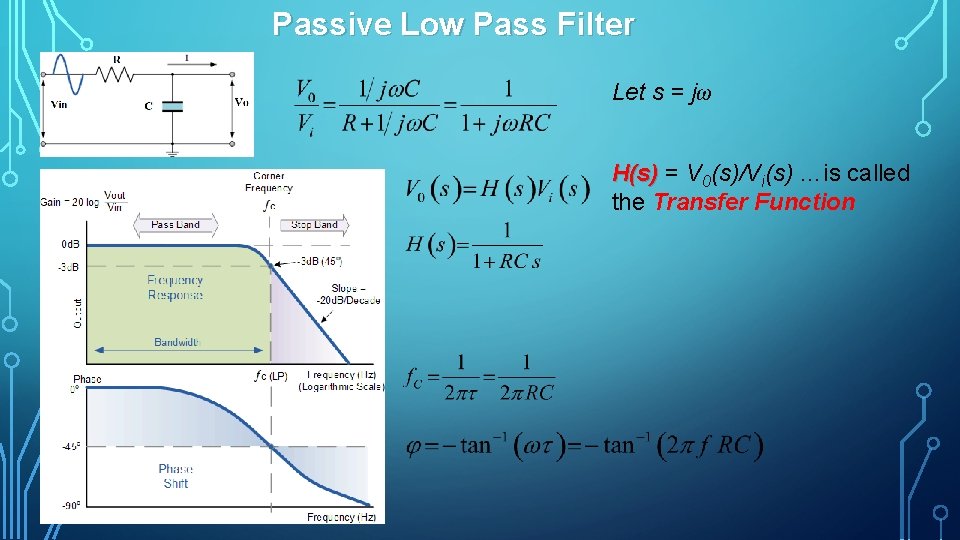
Passive Low Pass Filter Let s = jω H(s) = V H(s) 0(s)/Vi(s) …is called the Transfer Function
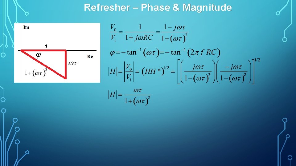
Refresher – Phase & Magnitude 1 φ
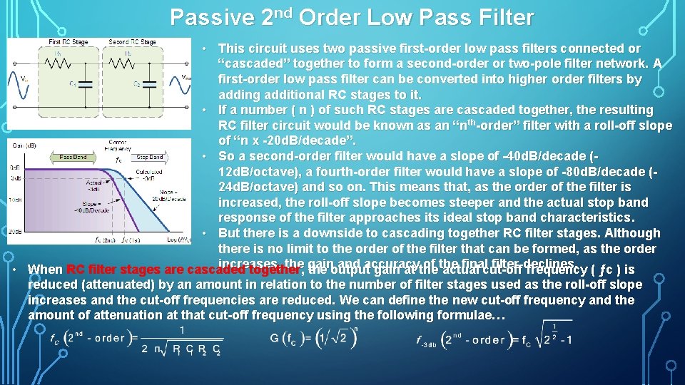
Passive 2 nd Order Low Pass Filter • This circuit uses two passive first order low pass filters connected or “cascaded” together to form a second order or two pole filter network. A first order low pass filter can be converted into higher order filters by adding additional RC stages to it. • If a number ( n ) of such RC stages are cascaded together, the resulting RC filter circuit would be known as an “nth order” filter with a roll off slope of “n x 20 d. B/decade”. • So a second order filter would have a slope of 40 d. B/decade ( 12 d. B/octave), a fourth order filter would have a slope of 80 d. B/decade ( 24 d. B/octave) and so on. This means that, as the order of the filter is increased, the roll off slope becomes steeper and the actual stop band response of the filter approaches its ideal stop band characteristics. • But there is a downside to cascading together RC filter stages. Although there is no limit to the order of the filter that can be formed, as the order increases, the gain and accuracy of the final filter . • When RC filter stages are cascaded together , the output gain at the actual cut off declines frequency ( ƒc ) is reduced (attenuated) by an amount in relation to the number of filter stages used as the roll off slope increases and the cut off frequencies are reduced. We can define the new cut off frequency and the amount of attenuation at that cut off frequency using the following formulae…
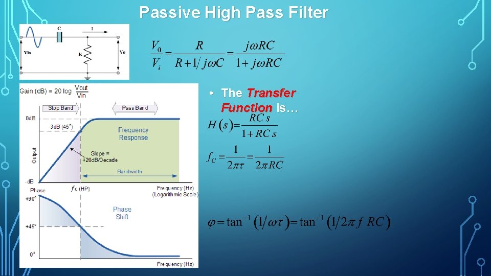
Passive High Pass Filter • The Transfer Function is…
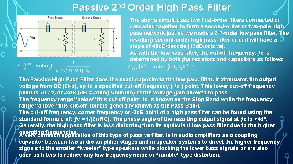
Passive 2 nd Order High Pass Filter The above circuit uses two first order filters connected or cascaded together to form a second order or two pole high pass network just as we made a 2 nd order low pass filter. The resulting second order high pass filter circuit will have a slope of 40 d. B/decade (12 d. B/octave). As with the low pass filter, the cut off frequency, ƒc is determined by both the resistors and capacitors as follows. The Passive High Pass Filter does the exact opposite to the low pass filter. It attenuates the output voltage from DC (0 Hz), up to a specified cut off frequency ( ƒc ) point. This lower cut off frequency point is 70. 7% or 3 d. B (d. B = 20 log Vout/Vin) of the voltage gain allowed to pass. The frequency range “below” this cut off point ƒc is known as the Stop Band while the frequency range “above” this cut off point is generally known as the Pass Band. The cut off frequency, corner frequency or 3 d. B point of a high pass filter can be found using the standard formula of: ƒc = 1/(2πRC). The phase angle of the resulting output signal at ƒc is +45 o. Generally, the high pass filter is less distorting than its equivalent low pass filter due to the higher operating frequencies. A very common application of this type of passive filter, is in audio amplifiers as a coupling capacitor between two audio amplifier stages and in speaker systems to direct the higher frequency signals to the smaller “tweeter” type speakers while blocking the lower bass signals or are also used as filters to reduce any low frequency noise or “rumble” type distortion.
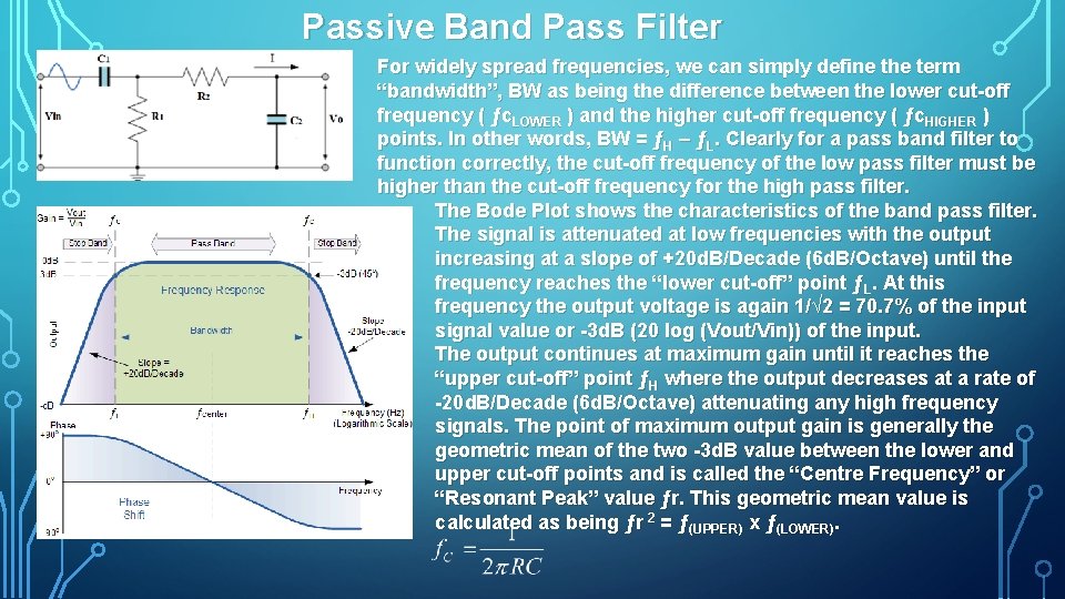
Passive Band Pass Filter For widely spread frequencies, we can simply define the term “bandwidth”, BW as being the difference between the lower cut off frequency ( ƒc. LOWER ) and the higher cut off frequency ( ƒc. HIGHER ) points. In other words, BW = ƒH – ƒL. Clearly for a pass band filter to function correctly, the cut off frequency of the low pass filter must be higher than the cut off frequency for the high pass filter. The Bode Plot shows the characteristics of the band pass filter. The signal is attenuated at low frequencies with the output increasing at a slope of +20 d. B/Decade (6 d. B/Octave) until the frequency reaches the “lower cut off” point ƒL. At this frequency the output voltage is again 1/√ 2 = 70. 7% of the input signal value or 3 d. B (20 log (Vout/Vin)) of the input. The output continues at maximum gain until it reaches the “upper cut off” point ƒH where the output decreases at a rate of 20 d. B/Decade (6 d. B/Octave) attenuating any high frequency signals. The point of maximum output gain is generally the geometric mean of the two 3 d. B value between the lower and upper cut off points and is called the “Centre Frequency” or “Resonant Peak” value ƒr. This geometric mean value is calculated as being ƒr 2 = ƒ(UPPER) x ƒ(LOWER).
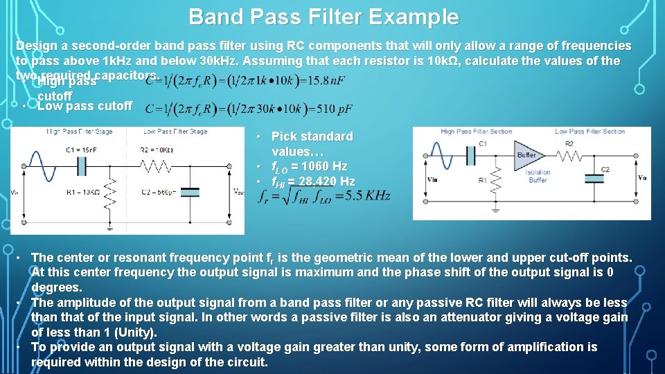
Band Pass Filter Example Design a second order band pass filter using RC components that will only allow a range of frequencies to pass above 1 k. Hz and below 30 k. Hz. Assuming that each resistor is 10 kΩ, calculate the values of the two required capacitors. • High pass cutoff • Low pass cutoff • Pick standard values… • f. LO = 1060 Hz • f. HI = 28, 420 Hz • The center or resonant frequency point fr is the geometric mean of the lower and upper cut off points. At this center frequency the output signal is maximum and the phase shift of the output signal is 0 degrees. • The amplitude of the output signal from a band pass filter or any passive RC filter will always be less than that of the input signal. In other words a passive filter is also an attenuator giving a voltage gain of less than 1 (Unity). • To provide an output signal with a voltage gain greater than unity, some form of amplification is required within the design of the circuit.

Active Low Pass Filter The advantage here is that the op amp’s high input impedance prevents excessive loading on the filter’s output, while its low output impedance prevents any changes in load from affecting the filter’s cut off frequency point. This configuration provides good filter stability, but its it has a maximum voltage gain limited to unity. However, the power gain is very high as its output impedance is much lower than its input impedance. If a voltage gain greater than one is required we can use the following filter circuit… The frequency response of the circuit will be the same as that for the passive RC filter, except that the amplitude of the output is increased by the pass band gain, AV of the amplifier. The transfer function H(s) is identical to that of a passive low pass, except it’s modified by the pass band gain, AF , of the active filter. You should convince yourself that the magnitude of the gain as a function of frequency can be written as…
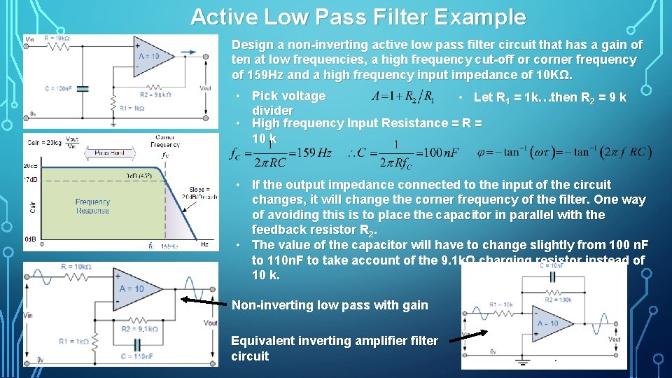
Active Low Pass Filter Example Design a non inverting active low pass filter circuit that has a gain of ten at low frequencies, a high frequency cut off or corner frequency of 159 Hz and a high frequency input impedance of 10 KΩ. • Pick voltage • Let R 1 = 1 k…then R 2 = 9 k divider • High frequency Input Resistance = R = 10 k • If the output impedance connected to the input of the circuit changes, it will change the corner frequency of the filter. One way of avoiding this is to place the capacitor in parallel with the feedback resistor R 2. • The value of the capacitor will have to change slightly from 100 n. F to 110 n. F to take account of the 9. 1 kΩ charging resistor instead of 10 k. Non inverting low pass with gain Equivalent inverting amplifier filter circuit
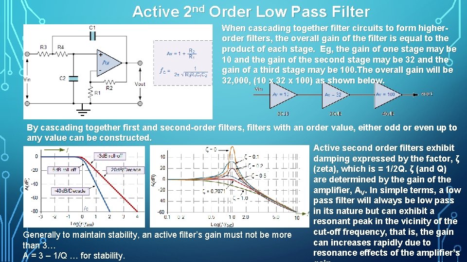
Active 2 nd Order Low Pass Filter When cascading together filter circuits to form higher order filters, the overall gain of the filter is equal to the product of each stage. Eg, the gain of one stage may be 10 and the gain of the second stage may be 32 and the gain of a third stage may be 100. The overall gain will be 32, 000, (10 x 32 x 100) as shown below. By cascading together first and second order filters, filters with an order value, either odd or even up to any value can be constructed. Active second order filters exhibit damping expressed by the factor, ζ (zeta), which is = 1/2 Q. ζ (and Q) are determined by the gain of the amplifier, AV. In simple terms, a low pass filter will always be low pass in its nature but can exhibit a resonant peak in the vicinity of the cut off frequency, that is, the gain Generally to maintain stability, an active filter’s gain must not be more can increases rapidly due to than 3… resonance effects of the amplifier’s A = 3 – 1/Q … for stability.
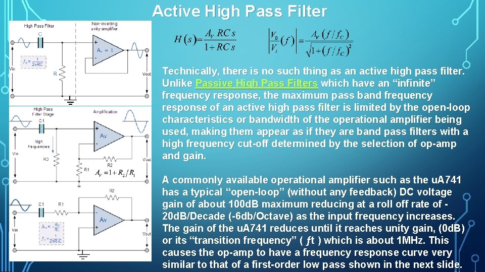
Active High Pass Filter Technically, there is no such thing as an active high pass filter. Unlike Passive High Pass Filters which have an “infinite” frequency response, the maximum pass band frequency response of an active high pass filter is limited by the open loop characteristics or bandwidth of the operational amplifier being used, making them appear as if they are band pass filters with a high frequency cut off determined by the selection of op amp and gain. A commonly available operational amplifier such as the u. A 741 has a typical “open loop” (without any feedback) DC voltage gain of about 100 d. B maximum reducing at a roll off rate of 20 d. B/Decade ( 6 db/Octave) as the input frequency increases. The gain of the u. A 741 reduces until it reaches unity gain, (0 d. B) or its “transition frequency” ( ƒt ) which is about 1 MHz. This causes the op amp to have a frequency response curve very similar to that of a first order low pass shown in the next slide.
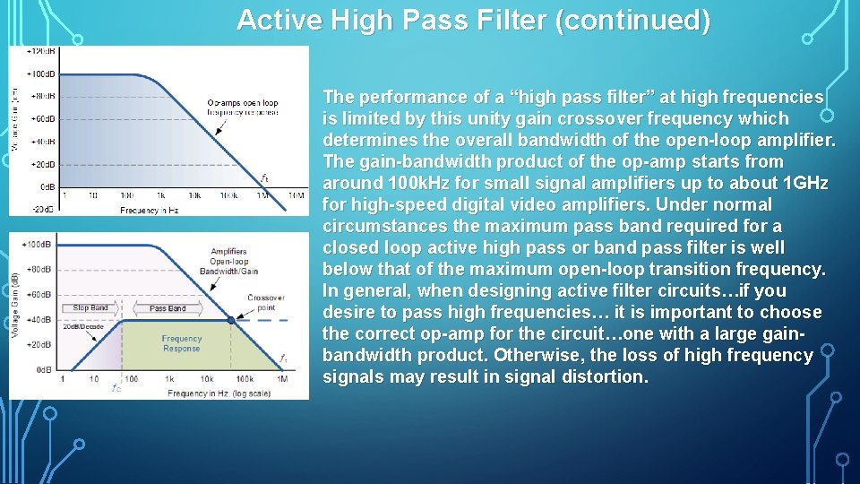
Active High Pass Filter (continued) The performance of a “high pass filter” at high frequencies is limited by this unity gain crossover frequency which determines the overall bandwidth of the open loop amplifier. The gain bandwidth product of the op amp starts from around 100 k. Hz for small signal amplifiers up to about 1 GHz for high speed digital video amplifiers. Under normal circumstances the maximum pass band required for a closed loop active high pass or band pass filter is well below that of the maximum open loop transition frequency. In general, when designing active filter circuits…if you desire to pass high frequencies… it is important to choose the correct op amp for the circuit…one with a large gain bandwidth product. Otherwise, the loss of high frequency signals may result in signal distortion.
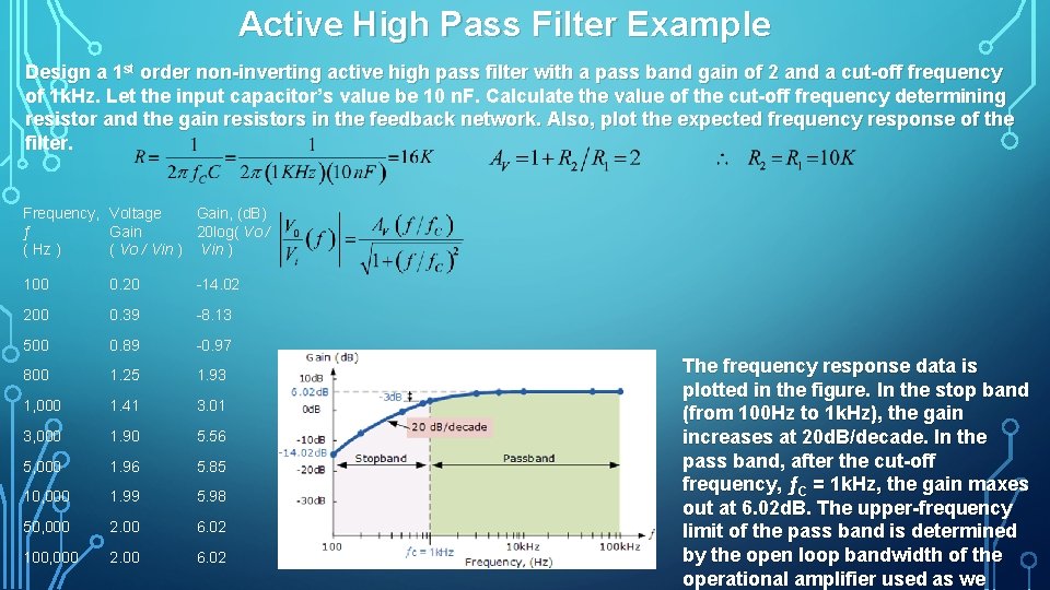
Active High Pass Filter Example Design a 1 st order non inverting active high pass filter with a pass band gain of 2 and a cut off frequency of 1 k. Hz. Let the input capacitor’s value be 10 n. F. Calculate the value of the cut off frequency determining resistor and the gain resistors in the feedback network. Also, plot the expected frequency response of the filter. Frequency, Voltage Gain, (d. B) ƒ Gain 20 log( Vo / ( Hz ) ( Vo / Vin ) 100 0. 20 -14. 02 200 0. 39 -8. 13 500 0. 89 -0. 97 800 1. 25 1. 93 1, 000 1. 41 3. 01 3, 000 1. 90 5. 56 5, 000 1. 96 5. 85 10, 000 1. 99 5. 98 50, 000 2. 00 6. 02 100, 000 2. 00 6. 02 The frequency response data is plotted in the figure. In the stop band (from 100 Hz to 1 k. Hz), the gain increases at 20 d. B/decade. In the pass band, after the cut off frequency, ƒC = 1 k. Hz, the gain maxes out at 6. 02 d. B. The upper frequency limit of the pass band is determined by the open loop bandwidth of the operational amplifier used as we
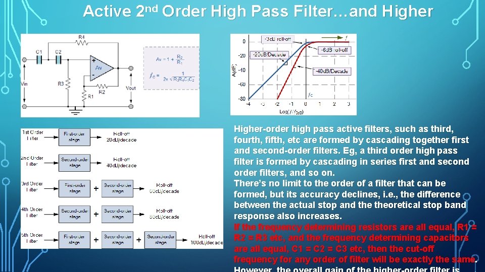
Active 2 nd Order High Pass Filter…and Higher order high pass active filters, such as third, fourth, fifth, etc are formed by cascading together first and second order filters. Eg, a third order high pass filter is formed by cascading in series first and second order filters, and so on. There’s no limit to the order of a filter that can be formed, but its accuracy declines, i. e. , the difference between the actual stop and theoretical stop band response also increases. If the frequency determining resistors are all equal, R 1 = R 2 = R 3 etc, and the frequency determining capacitors are all equal, C 1 = C 2 = C 3 etc, then the cut off frequency for any order of filter will be exactly the same.
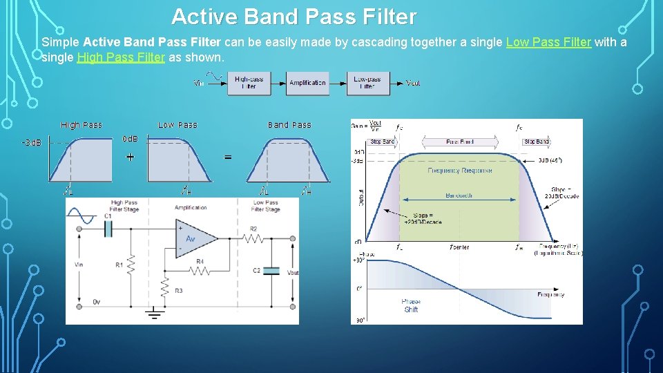
Active Band Pass Filter Simple Active Band Pass Filter can be easily made by cascading together a single Low Pass Filter with a single High Pass Filter as shown.
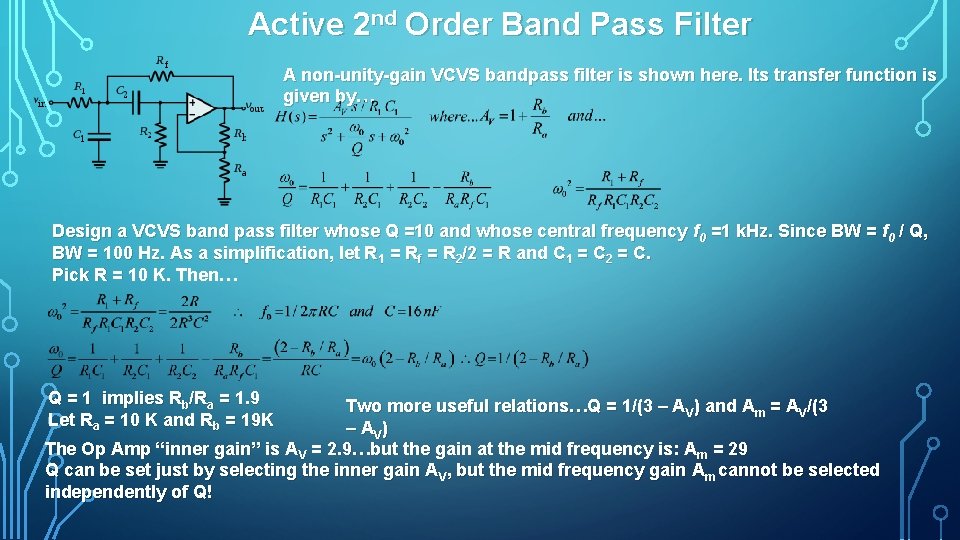
Active 2 nd Order Band Pass Filter A non unity gain VCVS bandpass filter is shown here. Its transfer function is given by… Design a VCVS band pass filter whose Q =10 and whose central frequency f 0 =1 k. Hz. Since BW = f 0 / Q, BW = 100 Hz. As a simplification, let R 1 = Rf = R 2/2 = R and C 1 = C 2 = C. Pick R = 10 K. Then… Q = 1 implies Rb/Ra = 1. 9 Let Ra = 10 K and Rb = 19 K Two more useful relations…Q = 1/(3 – AV) and Am = AV/(3 – AV) The Op Amp “inner gain” is AV = 2. 9…but the gain at the mid frequency is: Am = 29 Q can be set just by selecting the inner gain AV, but the mid frequency gain Am cannot be selected independently of Q!
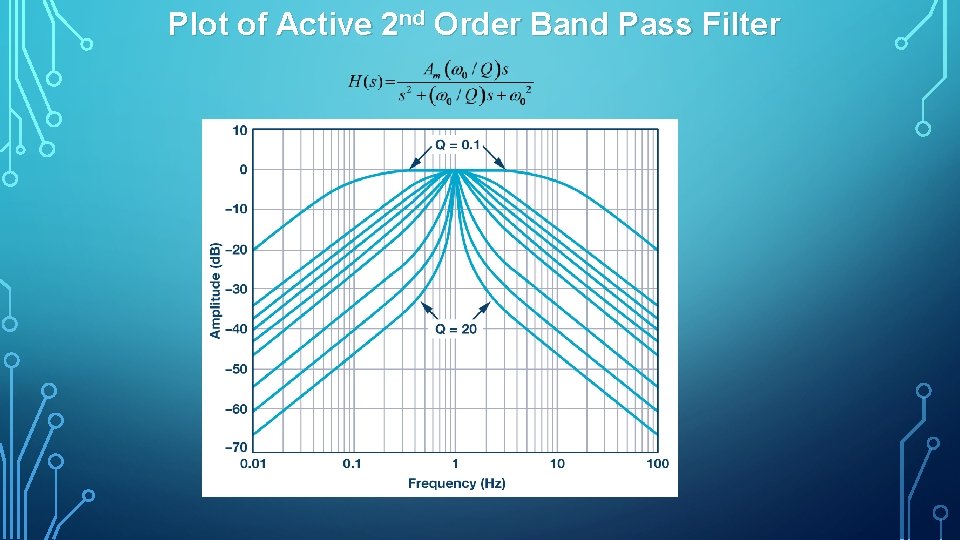
Plot of Active 2 nd Order Band Pass Filter
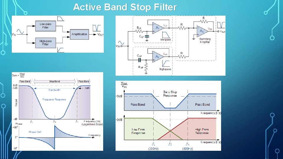
Active Band Stop Filter
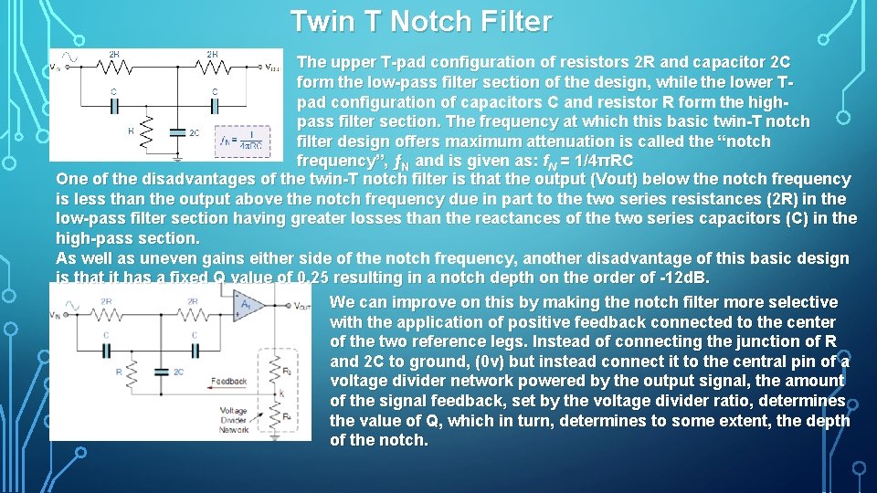
Twin T Notch Filter The upper T pad configuration of resistors 2 R and capacitor 2 C form the low pass filter section of the design, while the lower T pad configuration of capacitors C and resistor R form the high pass filter section. The frequency at which this basic twin T notch filter design offers maximum attenuation is called the “notch frequency”, ƒN and is given as: f. N = 1/4πRC One of the disadvantages of the twin T notch filter is that the output (Vout) below the notch frequency is less than the output above the notch frequency due in part to the two series resistances (2 R) in the low pass filter section having greater losses than the reactances of the two series capacitors (C) in the high pass section. As well as uneven gains either side of the notch frequency, another disadvantage of this basic design is that it has a fixed Q value of 0. 25 resulting in a notch depth on the order of 12 d. B. We can improve on this by making the notch filter more selective with the application of positive feedback connected to the center of the two reference legs. Instead of connecting the junction of R and 2 C to ground, (0 v) but instead connect it to the central pin of a voltage divider network powered by the output signal, the amount of the signal feedback, set by the voltage divider ratio, determines the value of Q, which in turn, determines to some extent, the depth of the notch.

Response of Different Filter Types Transfer function for a 2 nd order low pass and high pass filters… The values of the R’s and C’s used in a second order filter determine the coefficients of the 2 nd order polynomial in the filter’s transfer function. Eg, if the values are selected to generate 2 nd order Butterworth, Chebyshev, Elliptic or Bessel function polynomials then you get that type of filter. • Butterworth: Flattest pass band but a poor roll off rate. • Chebyshev: Some pass band ripple but a better (steeper) roll off rate. • Elliptic: Some pass and stop band ripple but with the steepest roll off rate. • Bessel: Worst roll off rate of all four filters but the best phase response. Filters with a poor phase response will react poorly to a change in signal level.
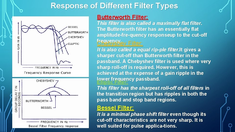
Response of Different Filter Types Butterworth Filter: This filter is also called a maximally flat filter. The Butterworth filter has an essentially flat amplitude fre quency response up to the cut off frequency. Chebyshev Filter: It is also called a equal rip ple filter. It gives a sharper cut off than Butterworth filter in the passband. A Chebyshev filter is used where very sharp roll off is required. However, this is achieved at the expense of a gain ripple in the lower frequency passband. Elliptic Filter: This filter has the sharpest roll off of all filters in the transition region but has ripples in both the pass band stop band regions. Bessel Filter: It is a minimal phase shift filter even though its cut off characteristics are not very sharp. It is well suited for pulse applica tions.
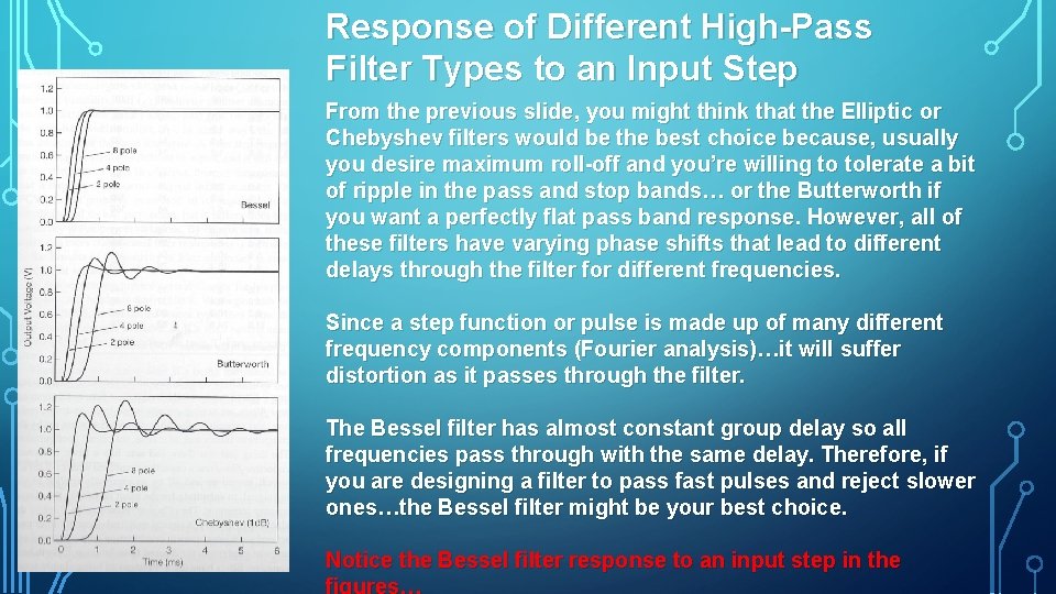
Response of Different High Pass Filter Types to an Input Step From the previous slide, you might think that the Elliptic or Chebyshev filters would be the best choice because, usually you desire maximum roll off and you’re willing to tolerate a bit of ripple in the pass and stop bands… or the Butterworth if you want a perfectly flat pass band response. However, all of these filters have varying phase shifts that lead to different delays through the filter for different frequencies. Since a step function or pulse is made up of many different frequency components (Fourier analysis)…it will suffer distortion as it passes through the filter. The Bessel filter has almost constant group delay so all frequencies pass through with the same delay. Therefore, if you are designing a filter to pass fast pulses and reject slower ones…the Bessel filter might be your best choice. Notice the Bessel filter response to an input step in the figures…
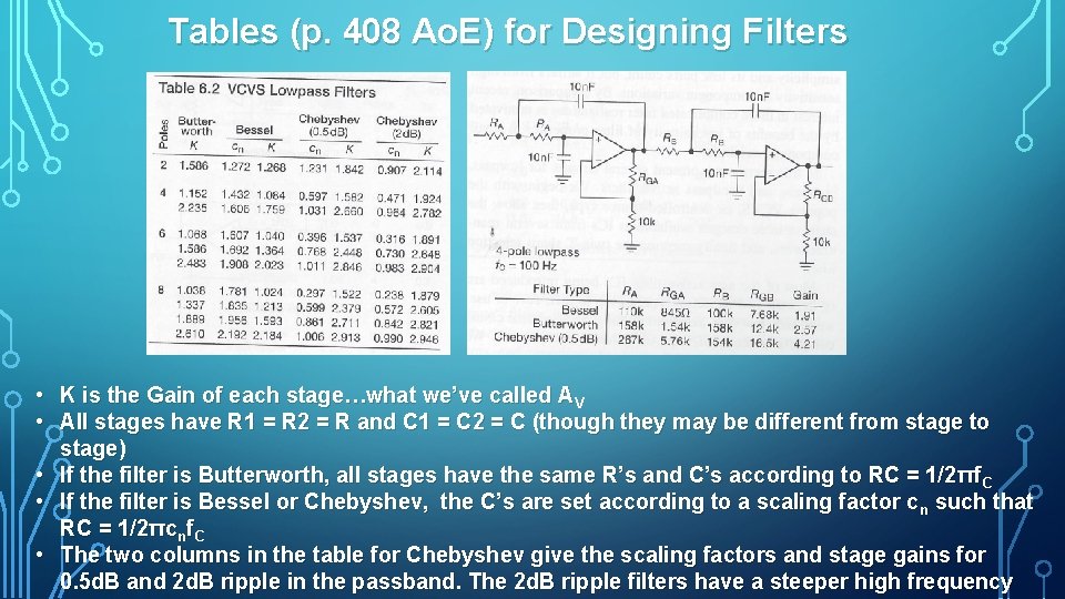
Tables (p. 408 Ao. E) for Designing Filters • K is the Gain of each stage…what we’ve called AV • All stages have R 1 = R 2 = R and C 1 = C 2 = C (though they may be different from stage to stage) • If the filter is Butterworth, all stages have the same R’s and C’s according to RC = 1/2 πf. C • If the filter is Bessel or Chebyshev, the C’s are set according to a scaling factor c n such that RC = 1/2πcnf. C • The two columns in the table for Chebyshev give the scaling factors and stage gains for 0. 5 d. B and 2 d. B ripple in the passband. The 2 d. B ripple filters have a steeper high frequency
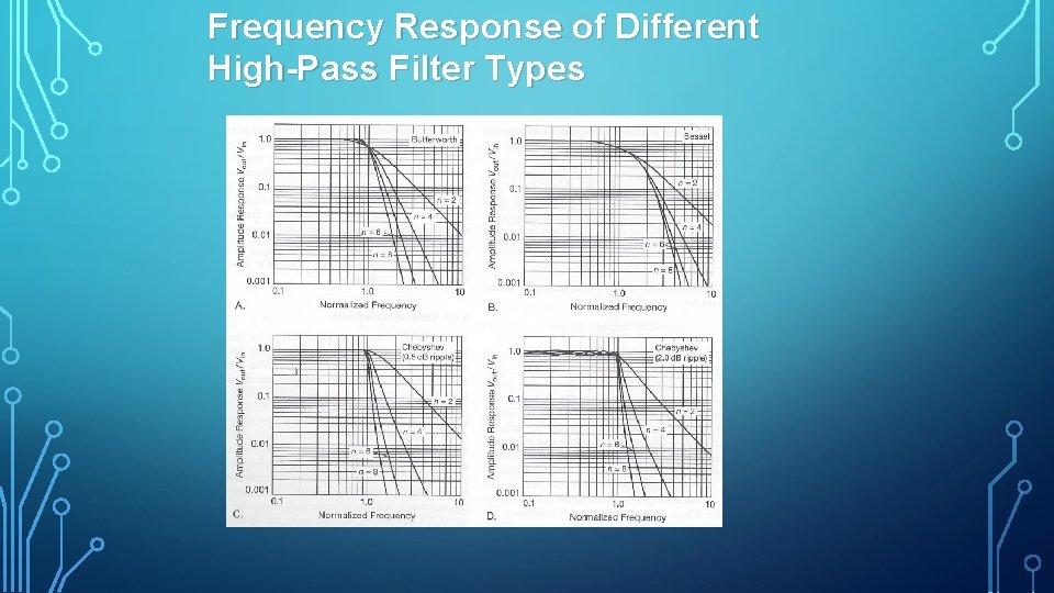
Frequency Response of Different High Pass Filter Types
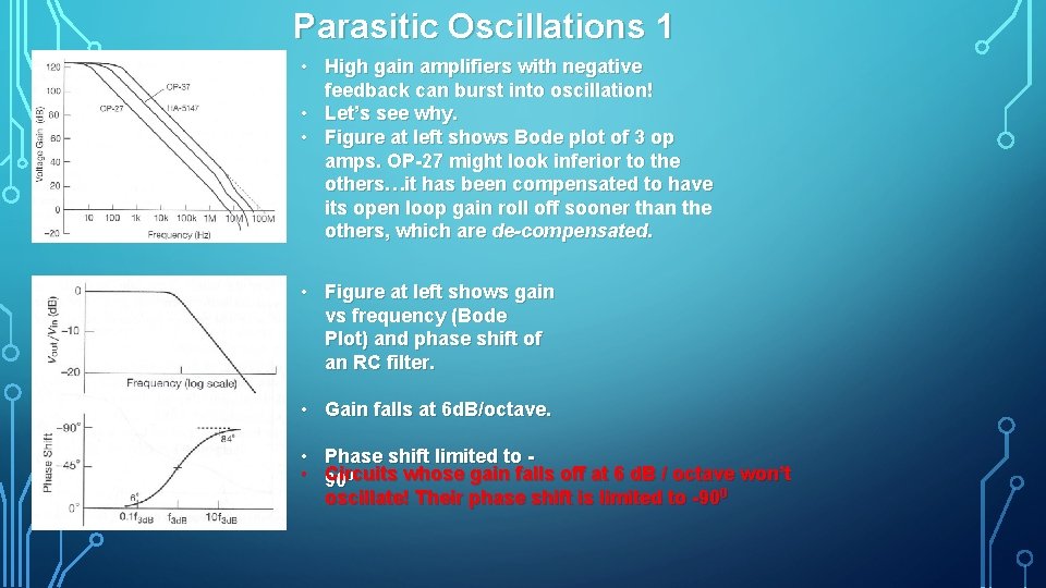
Parasitic Oscillations 1 • High gain amplifiers with negative feedback can burst into oscillation! • Let’s see why. • Figure at left shows Bode plot of 3 op amps. OP 27 might look inferior to the others…it has been compensated to have its open loop gain roll off sooner than the others, which are de compensated. • Figure at left shows gain vs frequency (Bode Plot) and phase shift of an RC filter. • Gain falls at 6 d. B/octave. • Phase shift limited to • Circuits whose gain falls off at 6 d. B / octave won’t 900 oscillate! Their phase shift is limited to 900
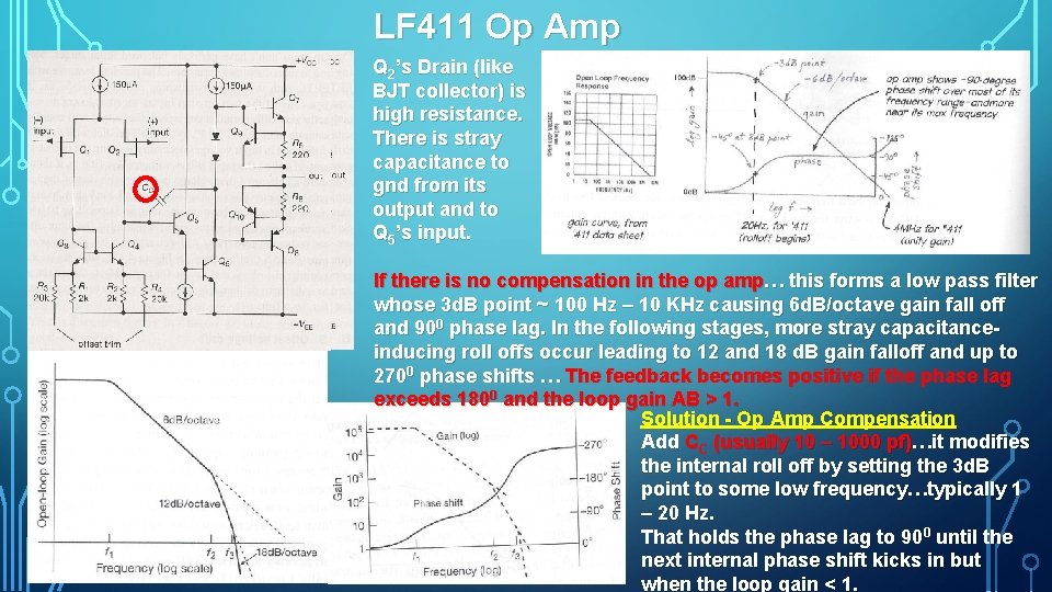
LF 411 Op Amp Q 2’s Drain (like BJT collector) is high resistance. There is stray capacitance to gnd from its output and to Q 5’s input. If there is no compensation in the op amp… this forms a low pass filter whose 3 d. B point ~ 100 Hz – 10 KHz causing 6 d. B/octave gain fall off and 900 phase lag. In the following stages, more stray capacitance inducing roll offs occur leading to 12 and 18 d. B gain falloff and up to 2700 phase shifts … The feedback becomes positive if the phase lag exceeds 1800 and the loop gain AB > 1. Solution Op Amp Compensation Add CC (usually 10 – 1000 pf)…it modifies the internal roll off by setting the 3 d. B point to some low frequency…typically 1 – 20 Hz. That holds the phase lag to 900 until the next internal phase shift kicks in but when the loop gain < 1.
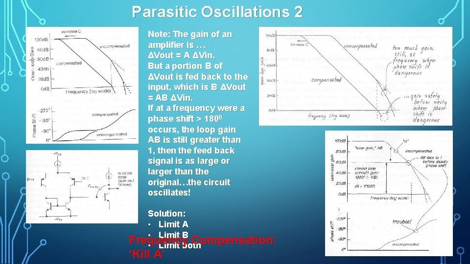
Parasitic Oscillations 2 Note: The gain of an amplifier is … ΔVout = A ΔVin. But a portion B of ΔVout is fed back to the input, which is B ΔVout = AB ΔVin. If at a frequency were a phase shift > 1800 occurs, the loop gain AB is still greater than 1, then the feed back signal is as large or larger than the original…the circuit oscillates! Solution: • Limit A • Limit B Frequency Compensation: • Limit both ‘Kill A’
- Slides: 29