Leakage and Dynamic Glitch Power Minimization Using MIP

- Slides: 19

Leakage and Dynamic Glitch Power Minimization Using MIP for Vth Assignment and Path Balancing Yuanlin Lu and Vishwani D. Agrawal Auburn University ECE Dept. , Auburn, Alabama, USA PATMOS’ 05, Leuven, Belgium, September 21 -23, 2005

Problem Statement § Design a CMOS Circuit : Ø with dual-threshold devices to globally minimize subthreshold leakage Ø with delay elements to eliminate all glitches Ø to maintain specified performance § Allow Performance-Power tradeoff 2

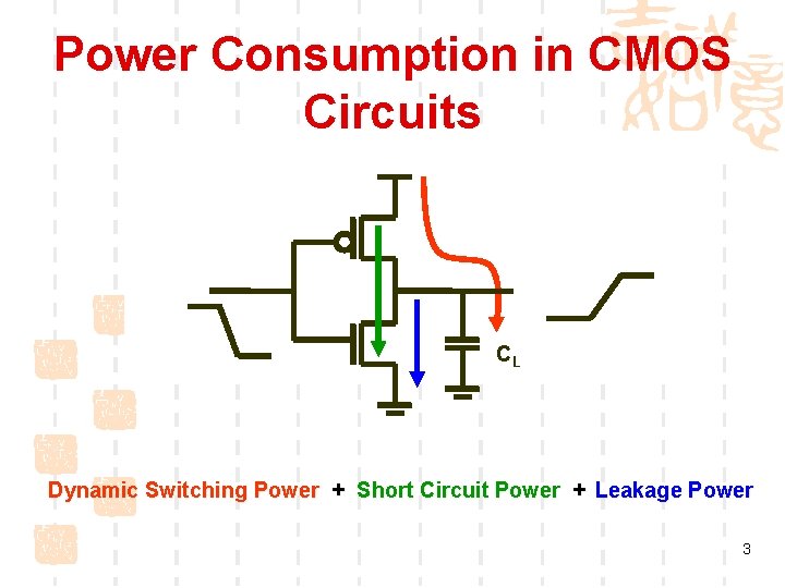
Power Consumption in CMOS Circuits CL Dynamic Switching Power + Short Circuit Power + Leakage Power 3

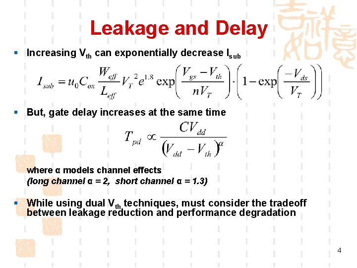
Leakage and Delay § Increasing Vth can exponentially decrease Isub § But, gate delay increases at the same time where α models channel effects (long channel α = 2, short channel α = 1. 3) § While using dual Vth techniques, must consider the tradeoff between leakage reduction and performance degradation 4

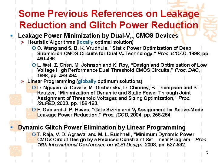
Some Previous References on Leakage Reduction and Glitch Power Reduction § Leakage Power Minimization by Dual-Vth CMOS Devices Ø Heuristic Algorithms (locally optimal solution) ¡ Q. Wang and S. B. K. Vrudhula, "Static Power Optimization of Deep Submicron CMOS Circuits for Dual VT Technology, " Proc. ICCAD, 1998, pp. 490 -496. ¡ L. Wei, Z. Chen, M. Johnson and K. Roy, “Design and Optimization of Low Voltage High Performance Dual Threshold CMOS Circuits, ” Proc. DAC, 1998, pp. 489 -494. Ø Linear Programming (globally optimum solutions) ¡ D. Nguyen, A. Davare, M. Orshansky, D. Chinney, B. Thompson and K. Keutzer, “Minimization of Dynamic and Static Power Through Joint Assignment of Threshold Voltages and Sizing Optimization, ” Proc. ISLPED, 2003, pp. 158 -163. ¡ F. Gao and J. P. Hayes, “Gate Sizing and Vt Assignment for Active-Mode Leakage Power Reduction, ” Proc. ICCD, 2004, pp. 258 -264 § Dynamic Glitch Power Elimination by Linear Programming ¡ T. Raja, V. D. Agrawal and M. L. Bushnell, “Minimum Dynamic Power CMOS Circuit Design by a Reduced Constraint Set Linear Program, ” Proc. 16 th International Conference on VLSI Design, 2003, pp. 527 -532. 5

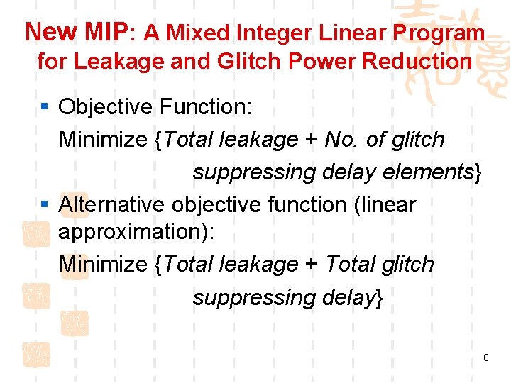
New MIP: A Mixed Integer Linear Program for Leakage and Glitch Power Reduction § Objective Function: Minimize {Total leakage + No. of glitch suppressing delay elements} § Alternative objective function (linear approximation): Minimize {Total leakage + Total glitch suppressing delay} 6

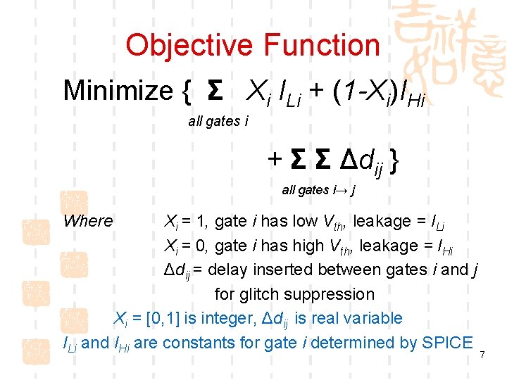
Objective Function Minimize { Σ Xi ILi + (1 -Xi)IHi all gates i + Σ Σ Δdij } all gates i→ j Where Xi = 1, gate i has low Vth, leakage = ILi Xi = 0, gate i has high Vth, leakage = IHi Δdij = delay inserted between gates i and j for glitch suppression Xi = [0, 1] is integer, Δdij is real variable ILi and IHi are constants for gate i determined by SPICE 7

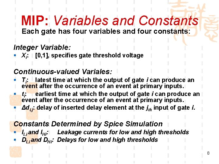
MIP: Variables and Constants Each gate has four variables and four constants: Integer Variable: § Xi: [0, 1], specifies gate threshold voltage Continuous-valued Variales: § Ti: latest time at which the output of gate i can produce an event after the occurrence of an event at primary inputs. § ti: earliest time at which the output of gate i can produce an event after the occurrence of an event at primary inputs. § Δdi, j: delay of inserted delay element at the jth input of gate i. Constants Determined by Spice Simulation § ILi and IHi: Leakage currents for low and high thresholds § DLi and DHi: Delays for low and high thresholds 8

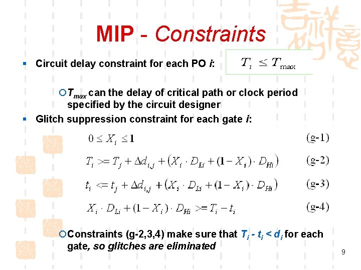
MIP - Constraints § Circuit delay constraint for each PO i: ¡ Tmax can the delay of critical path or clock period specified by the circuit designer § Glitch suppression constraint for each gate i: ¡ Constraints (g-2, 3, 4) make sure that Ti - ti < di for each gate, so glitches are eliminated 9

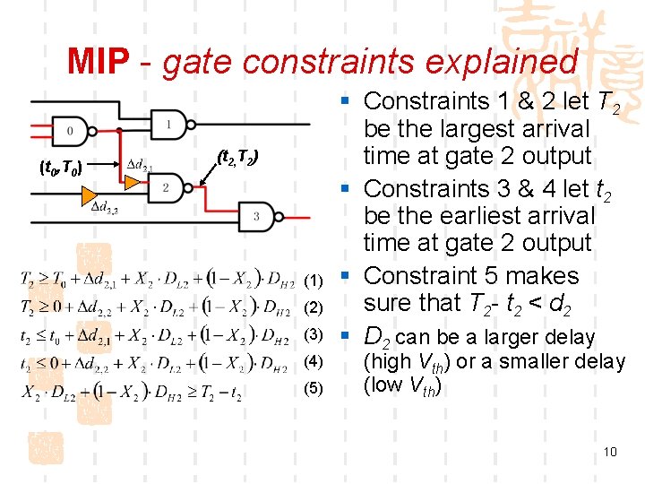
MIP - gate constraints explained (t 0, T 0) (t 2, T 2) (1) (2) (3) (4) (5) § Constraints 1 & 2 let T 2 be the largest arrival time at gate 2 output § Constraints 3 & 4 let t 2 be the earliest arrival time at gate 2 output § Constraint 5 makes sure that T 2 - t 2 < d 2 § D 2 can be a larger delay (high Vth) or a smaller delay (low Vth) 10

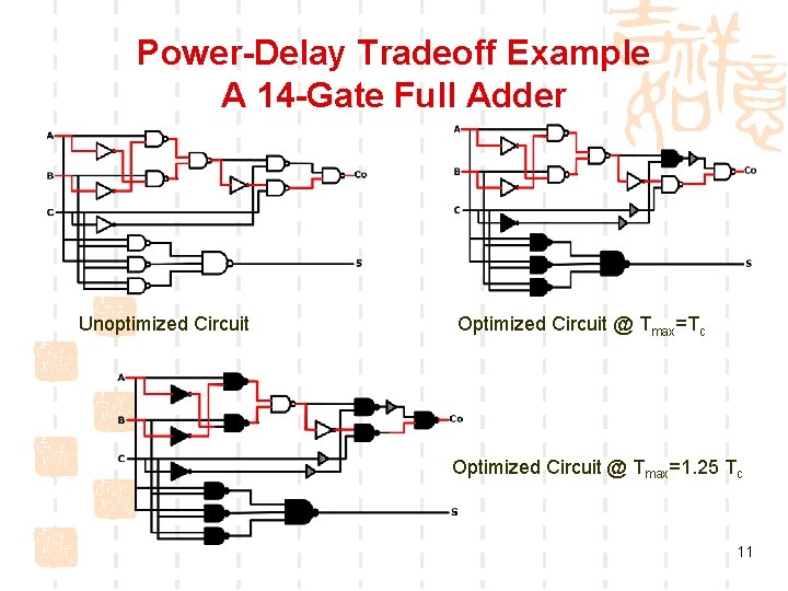
Power-Delay Tradeoff Example A 14 -Gate Full Adder Unoptimized Circuit Optimized Circuit @ Tmax=Tc Optimized Circuit @ Tmax=1. 25 Tc 11

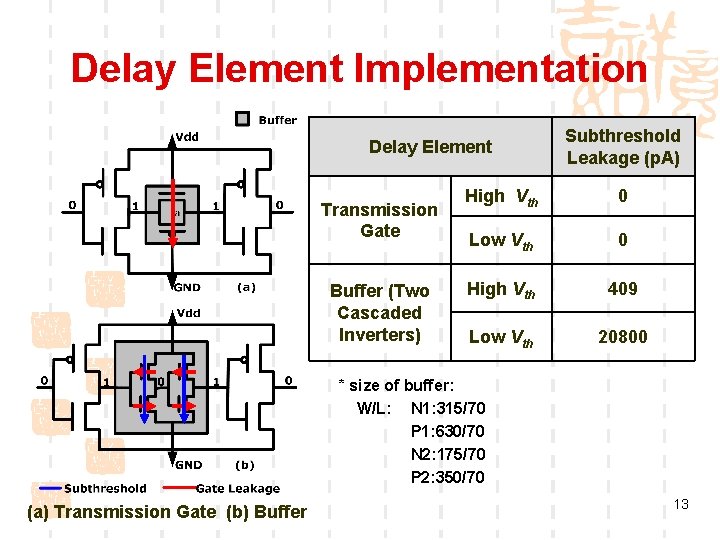
Choices for a Delay Element § Two cascaded-inverter buffer - consumes additional subthreshold leakage and dynamic power: § All delay buffers are on non-critical paths and are assigned high Vth, to reduce leakage overhead § Transmission gate (on state) – increases resistance § Smaller area overhead § No subthreshold leakage § Possible capacitance increase § Used before § T. Raja, V. D. Agrawal and M. L. Bushnell, “Variable Input Delay CMOS Logic for Low Power Design, ” Proc. 18 th International Conference on VLSI Design, January 2005, pp. 598 -605. § T. Raja, V. D. Agrawal and M. L. Bushnell, “Variable Input Delay CMOS Logic Design for Low Dynamic Power Circuits, ” PATMOS’ 05. 12

Delay Element Implementation Delay Element Transmission Gate Buffer (Two Cascaded Inverters) Subthreshold Leakage (p. A) High Vth 0 Low Vth 0 High Vth 409 Low Vth 20800 * size of buffer: W/L: N 1: 315/70 P 1: 630/70 N 2: 175/70 P 2: 350/70 (a) Transmission Gate (b) Buffer 13

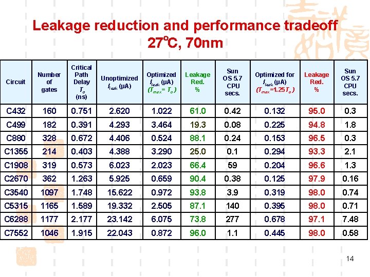
Leakage reduction and performance tradeoff 27℃, 70 nm Circuit Number of gates Critical Path Delay Tc (ns) C 432 160 C 499 Unoptimized Ileak (μA) Optimized Ileak (μA) (Tmax= Tc ) Leakage Red. % Sun OS 5. 7 CPU secs. Optimized for Ileak (μA) (Tmax=1. 25 Tc ) Leakage Red. % Sun OS 5. 7 CPU secs. 0. 751 2. 620 1. 022 61. 0 0. 42 0. 132 95. 0 0. 3 182 0. 391 4. 293 3. 464 19. 3 0. 08 0. 225 94. 8 1. 8 C 880 328 0. 672 4. 406 0. 524 88. 1 0. 24 0. 153 96. 5 0. 3 C 1355 214 0. 403 4. 388 3. 290 25. 0 0. 1 0. 294 93. 3 2. 1 C 1908 319 0. 573 6. 023 2. 023 66. 4 59 0. 204 96. 6 1. 3 C 2670 362 1. 263 5. 925 0. 659 90. 4 0. 38 0. 125 97. 9 0. 16 C 3540 1097 1. 748 15. 622 0. 972 93. 8 3. 9 0. 319 98. 0 0. 74 C 5315 1165 1. 589 19. 332 2. 505 87. 1 140 0. 395 98. 0 0. 71 C 6288 1177 23. 142 6. 075 73. 8 277 0. 678 97. 1 7. 48 C 7552 1046 1. 915 22. 043 0. 872 96. 0 1. 1 0. 445 98. 0 0. 58 14

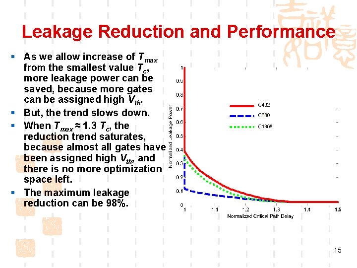
Leakage Reduction and Performance § As we allow increase of Tmax from the smallest value Tc, more leakage power can be saved, because more gates can be assigned high Vth. § But, the trend slows down. § When Tmax ≈ 1. 3 Tc, the reduction trend saturates, because almost all gates have been assigned high Vth, and there is no more optimization space left. § The maximum leakage reduction can be 98%. 15

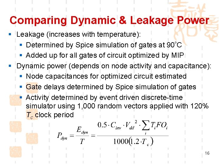
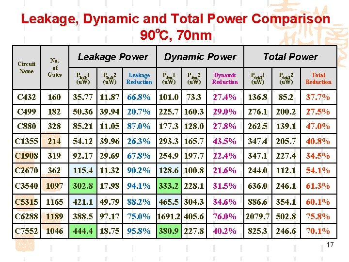
Comparing Dynamic & Leakage Power § Leakage (increases with temperature): § Determined by Spice simulation of gates at 90ºC § Added up for all gates of circuit optimized by MIP § Dynamic power (depends on node activity and capacitance): § Node capacitances for optimized circuit estimated § Gate delays determined by Spice simulation of gates § Activity determined by event driven discrete-time simulator using 1, 000 random vectors applied with 120% Tc clock period 16

Leakage, Dynamic and Total Power Comparison 90℃, 70 nm Circuit Name No. of Gates C 432 Leakage Power Dynamic Power Pleak 1 (u. W) Pdyn 1 (u. W) Pleak 2 (u. W) Leakage Reduction Total Power Pdyn 2 (u. W) Dynamic Reduction Ptotal 1 (u. W) Ptotal 2 (u. W) Total Reduction 160 35. 77 11. 87 66. 8% 101. 0 73. 3 27. 4% 136. 8 85. 2 37. 7% C 499 182 50. 36 39. 94 20. 7% 225. 7 160. 3 29. 0% 276. 1 200. 2 27. 5% C 880 328 85. 21 11. 05 87. 0% 177. 3 128. 0 27. 8% 262. 5 139. 1 47. 0% C 1355 214 54. 12 39. 96 26. 3% 293. 3 165. 7 43. 5% 347. 4 205. 7 40. 8% C 1908 319 92. 17 29. 69 67. 8% 254. 9 197. 7 22. 4% 347. 1 227. 4 34. 5% C 2670 362 115. 4 11. 32 90. 2% 128. 6 100. 8 21. 6% 244. 0 112. 1 54. 1% C 3540 1097 302. 8 17. 98 94. 1% 333. 2 228. 1 31. 5% 636. 0 246. 1 61. 3% C 5315 1165 421. 1 49. 79 88. 2% 465. 5 304. 3 34. 6% 886. 6 354. 1 60. 1% C 6288 1189 388. 5 97. 17 75. 0% 1691. 2 405. 6 76. 0% 2079. 7 502. 8 75. 8% C 7552 1046 444. 4 18. 75 95. 8% 380. 9 227. 8 40. 2% 70. 1% 825. 3 246. 6 17

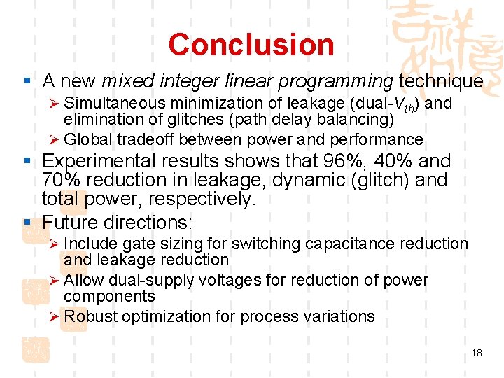
Conclusion § A new mixed integer linear programming technique Ø Simultaneous minimization of leakage (dual-Vth) and elimination of glitches (path delay balancing) Ø Global tradeoff between power and performance § Experimental results shows that 96%, 40% and 70% reduction in leakage, dynamic (glitch) and total power, respectively. § Future directions: Ø Include gate sizing for switching capacitance reduction and leakage reduction Ø Allow dual-supply voltages for reduction of power components Ø Robust optimization for process variations 18

Thank You All ! Questions?