LDMOS for RF Power Amplifiers David Fernandez Outline
- Slides: 12

LDMOS for RF Power Amplifiers David Fernandez

Outline Power Amplifier Critical Factors for Performance n LDMOS Device Technology n LDMOS Power Amplifier performance n Future trends and challenges for LDMOS n References n

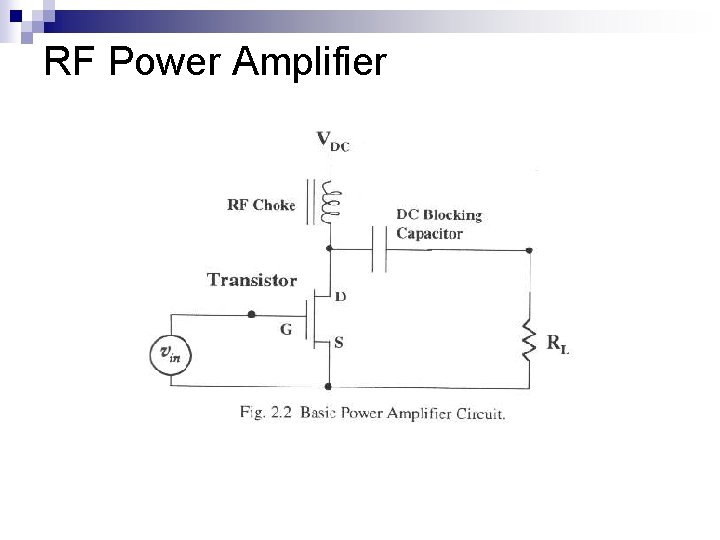
RF Power Amplifier

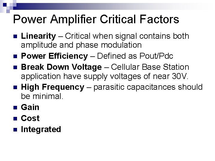
Power Amplifier Critical Factors n n n n Linearity – Critical when signal contains both amplitude and phase modulation Power Efficiency – Defined as Pout/Pdc Break Down Voltage – Cellular Base Station application have supply voltages of near 30 V. High Frequency – parasitic capacitances should be minimal. Gain Cost Integrated

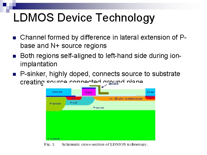
LDMOS Device Technology n n n Channel formed by difference in lateral extension of Pbase and N+ source regions Both regions self-aligned to left-hand side during ionimplantation P-sinker, highly doped, connects source to substrate creating source connected ground plane

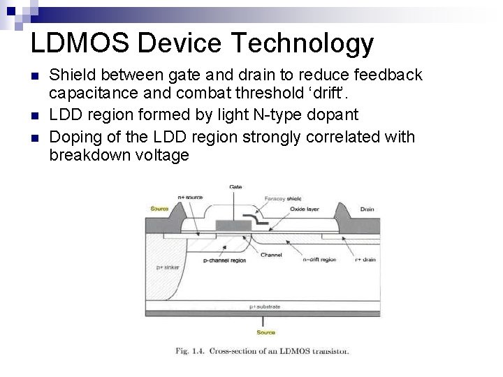
LDMOS Device Technology n n n Shield between gate and drain to reduce feedback capacitance and combat threshold ‘drift’. LDD region formed by light N-type dopant Doping of the LDD region strongly correlated with breakdown voltage

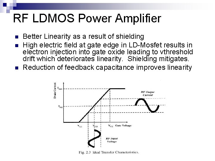
RF LDMOS Power Amplifier n n n Better Linearity as a result of shielding High electric field at gate edge in LD-Mosfet results in electron injection into gate oxide leading to vthreshold drift which deteriorates linearity. Shielding mitigates. Reduction of feedback capacitance improves linearity

RF LDMOS Power Amplifier n n n Better Gain and Cost accomplished through directly grounding source. With direct source grounding as compared to other power mosfets, no inductive bond-wires needed to connect source to package ground terminal. Source inductance deteriorates gain at high frequencies. No complex and costly packaging needed to keep drain insulated from ground terminal – drain and ground terminal are on opposite sides of wafer.

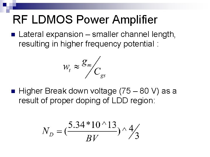
RF LDMOS Power Amplifier n Lateral expansion – smaller channel length, resulting in higher frequency potential : n Higher Break down voltage (75 – 80 V) as a result of proper doping of LDD region:

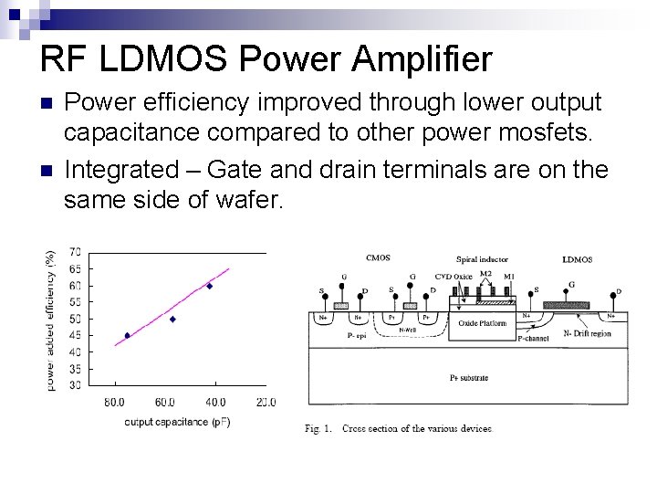
RF LDMOS Power Amplifier n n Power efficiency improved through lower output capacitance compared to other power mosfets. Integrated – Gate and drain terminals are on the same side of wafer.

Challenges and future trends n n Continued device innovations has led to 7 th generation LDMOS Power Mosfets that provide improved RF performance and remain low-cost. Thermal resistance as decreased and as a result the reliability of these devices is improved. Linearity has improved through both circuit and device design approaches. Currently compound semi-conductor devices (Ga. N) offer comparable if not improved efficiency and linearity, however cost and reliability issues make it difficult to displace LDMOS in the near future.

References n n n “Silicon RF Power Mosfets, ” B Jayant Baliga “RF Power Amplifiers for Wireless Communications, ” Steve Cripps “Challenges and Opportunities for Compound semiconductor devices in Next Generation Wireless Base Stations Power Amplifiers, ” Lawrence Lawson IEEE 2005 “Status and Trends of silicon LDMOS base station PA technologies to go beyond 2. 5 GHz applications, ” F. Van Rijs IEEE 2008 “A LDMOS Technology Compatible with CMOS and Passive Components for Integrated for RF Power Amplifiers, ” Jun Cai et. al, IEEE 2000