
LCFI Status Report Konstantin Stefanov on behalf of
LCFI Status Report Konstantin Stefanov on behalf of LCFI CALICE UK Meeting, 27 March 2007 v Introduction v LCFI Vertex Package v Vertex Detector R&D l Column-Parallel CCDs l In-situ Storage Image Sensors l Mechanical support studies v Areas of Common Interest for LCFI and CALICE v Conclusion Konstantin Stefanov, Rutherford Appleton Laboratory 1
Vertex Package – Overview (based on Sonja’s presentations) Goal: l Evaluation of the performance of the vertex detector and optimisation of its parameters l Development of tools l Studies of benchmark physics processes l Vertex Package interfaces to the Marlin. Reco framework, adding important and so far missing contribution l Framework consists of software modules (processors) l Enabled and configured via XML file l Path towards full MC simulation and reconstruction (MOKKA + Marlin. Reco) l Developed by Ben Jeffery and Erik Devetak (Oxford), Mark Grimes (Bristol), under the leadership of Sonja Hillert (Oxford) Konstantin Stefanov, Rutherford Appleton Laboratory 2
Vertex Package – Status: l Fully functional l 20, 000 lines of C++ code l Currently finalising issues with integration with the MARLIN framework and verifying performance l Release is expected any time now l Eagerly awaited worldwide l After the release: v Will move to using full pattern recognition in Marlin. Reco, including all silicon detectors and the TPC (currently uses track cheaters) v Use more realistic Vertex detector geometry (ladders) instead of cylinders l Tutorials for new users to be held starting in May Konstantin Stefanov, Rutherford Appleton Laboratory 3
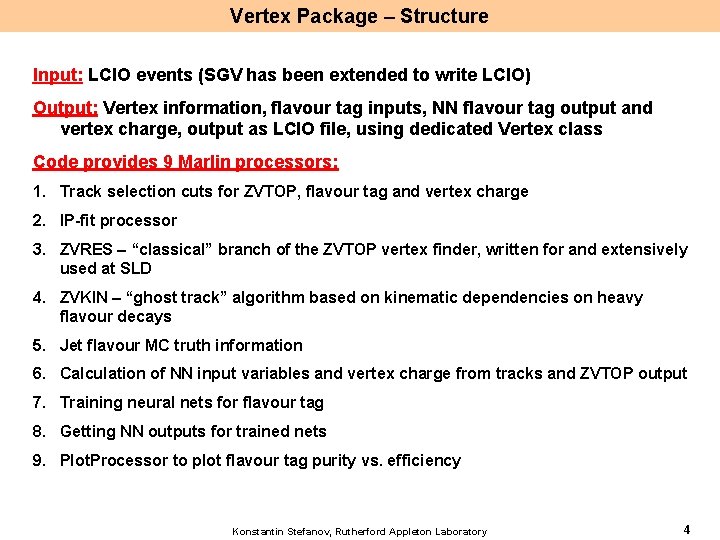
Vertex Package – Structure Input: LCIO events (SGV has been extended to write LCIO) Output: Vertex information, flavour tag inputs, NN flavour tag output and vertex charge, output as LCIO file, using dedicated Vertex class Code provides 9 Marlin processors: 1. Track selection cuts for ZVTOP, flavour tag and vertex charge 2. IP-fit processor 3. ZVRES – “classical” branch of the ZVTOP vertex finder, written for and extensively used at SLD 4. ZVKIN – “ghost track” algorithm based on kinematic dependencies on heavy flavour decays 5. Jet flavour MC truth information 6. Calculation of NN input variables and vertex charge from tracks and ZVTOP output 7. Training neural nets for flavour tag 8. Getting NN outputs for trained nets 9. Plot. Processor to plot flavour tag purity vs. efficiency Konstantin Stefanov, Rutherford Appleton Laboratory 4
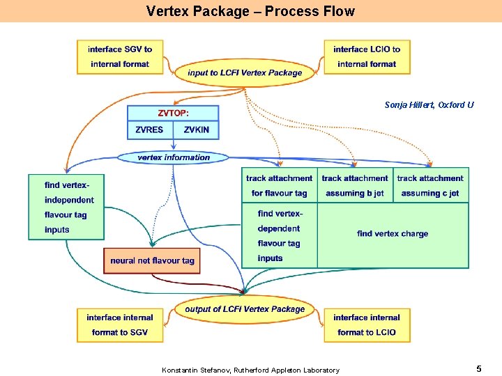
Vertex Package – Process Flow Sonja Hillert, Oxford U Konstantin Stefanov, Rutherford Appleton Laboratory 5
Vertex Package – Verification l Extensive verification over many months, a lot of hard work v 1 st stage: comparisons between SGV and MARLIN using identical input events (SGV and the old FORTRAN ZVTOP very well known) v 2 nd stage: v Same events from the 1 st stage (PYTHIA) passed through full MC simulation MOKKA v Collaboration with DESY and MPI Munich for production of the input data sample v Comparisons of MARLIN (MOKKA input) with MARLIN (SGV input) and former BRAHMS results from TESLA TDR v First indications: MARLIN (C++) slightly outperforms SGV (FORTRAN) l Debugging using the tool Valgrind http: //valgrind. org – helps find memory leaks, improves performance by using profilers l Documentation using Doxygen http: //www. doxygen. org – provides automatic documentation from commented C++ code Konstantin Stefanov, Rutherford Appleton Laboratory 6
Vertex Detector R&D What is required for the vertex detector at ILC: l Excellent point resolution (3. 5 μm), small pixel size = 20 μm, close to IP l Low material budget ( 0. 1% X 0 per layer), low power dissipation l Fast (low occupancy) readout – challenging, two main approaches l Column parallel readout during the 1 ms beam at 50 MHz (L 1) or 25 MHz (L 2 -L 5) l In-situ signal storage, readout in the 200 ms – long gap l Tolerates Electro-Magnetic Interference (EMI) What LCFI has done so far: l Made 2 generations of Column Parallel CCDs: CPC 1 and CPC 2 l In-situ Storage Image Sensor – proof of principle device ISIS 1 designed and tested l CMOS readout chips for CPC 1/2: 2 generations, bump bonded to the CCDs l Driver chip for CPC 2 designed and manufactured l Built lots of electronics to support the detectors l Extensive tests of stand-alone devices and hybrid bump-bonded assemblies Konstantin Stefanov, Rutherford Appleton Laboratory 7
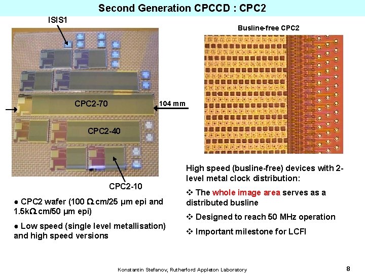
Second Generation CPCCD : CPC 2 ISIS 1 Busline-free CPC 2 -70 104 mm CPC 2 -40 CPC 2 -10 ● CPC 2 wafer (100 . cm/25 μm epi and 1. 5 k. cm/50 μm epi) ● Low speed (single level metallisation) and high speed versions High speed (busline-free) devices with 2 level metal clock distribution: v The whole image area serves as a distributed busline v Designed to reach 50 MHz operation v Important milestone for LCFI Konstantin Stefanov, Rutherford Appleton Laboratory 8
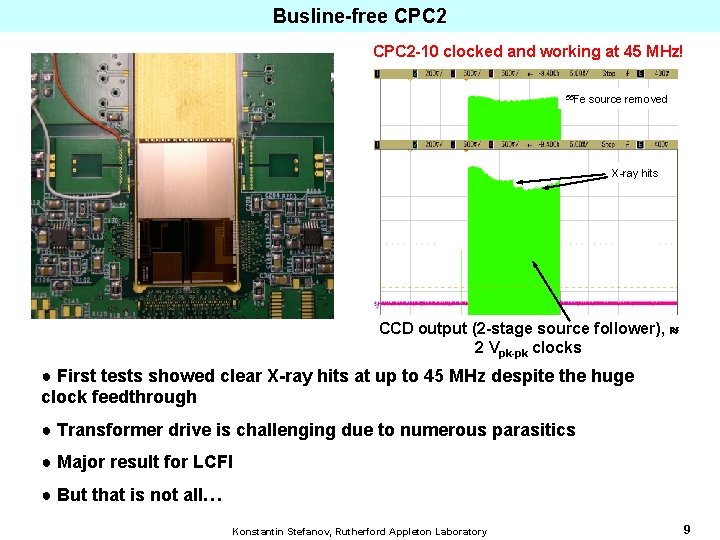
Busline-free CPC 2 -10 clocked and working at 45 MHz! 55 Fe source removed X-ray hits CCD output (2 -stage source follower), 2 Vpk-pk clocks ● First tests showed clear X-ray hits at up to 45 MHz despite the huge clock feedthrough ● Transformer drive is challenging due to numerous parasitics ● Major result for LCFI ● But that is not all… Konstantin Stefanov, Rutherford Appleton Laboratory 9
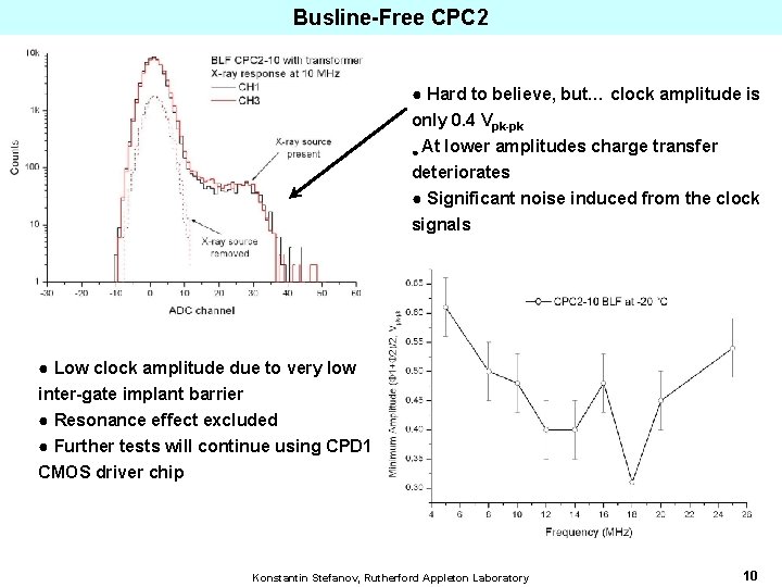
Busline-Free CPC 2 ● Hard to believe, but… clock amplitude is only 0. 4 Vpk-pk ● At lower amplitudes charge transfer deteriorates ● Significant noise induced from the clock signals ● Low clock amplitude due to very low inter-gate implant barrier ● Resonance effect excluded ● Further tests will continue using CPD 1 CMOS driver chip Konstantin Stefanov, Rutherford Appleton Laboratory 10
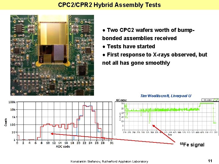
CPC 2/CPR 2 Hybrid Assembly Tests ● Two CPC 2 wafers worth of bumpbonded assemblies received ● Tests have started ● First response to X-rays observed, but not all has gone smoothly Tim Woolliscroft, Liverpool U 55 Fe Konstantin Stefanov, Rutherford Appleton Laboratory signal 11
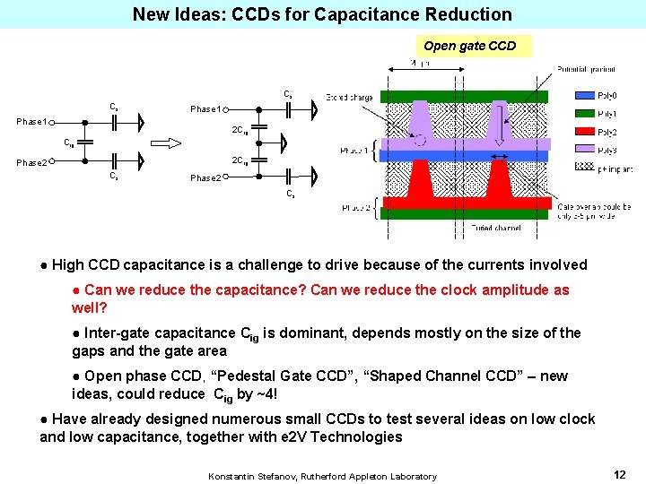
New Ideas: CCDs for Capacitance Reduction Open gate CCD Cs Cs Phase 1 2 Cig Phase 2 Cs ● High CCD capacitance is a challenge to drive because of the currents involved ● Can we reduce the capacitance? Can we reduce the clock amplitude as well? ● Inter-gate capacitance Cig is dominant, depends mostly on the size of the gaps and the gate area ● Open phase CCD, “Pedestal Gate CCD”, “Shaped Channel CCD” – new ideas, could reduce Cig by ~4! ● Have already designed numerous small CCDs to test several ideas on low clock and low capacitance, together with e 2 V Technologies Konstantin Stefanov, Rutherford Appleton Laboratory 12
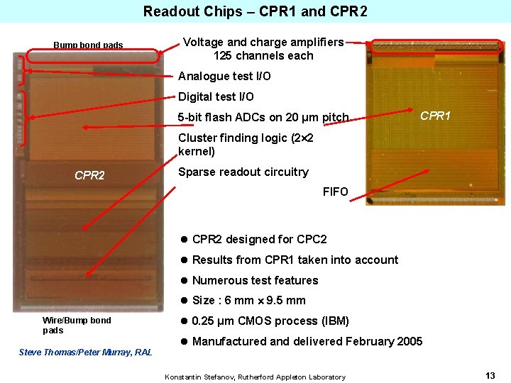
Readout Chips – CPR 1 and CPR 2 Bump bond pads Voltage and charge amplifiers 125 channels each Analogue test I/O Digital test I/O 5 -bit flash ADCs on 20 μm pitch CPR 1 Cluster finding logic (2 2 kernel) CPR 2 Sparse readout circuitry FIFO l CPR 2 designed for CPC 2 l Results from CPR 1 taken into account l Numerous test features l Size : 6 mm 9. 5 mm Wire/Bump bond pads Steve Thomas/Peter Murray, RAL l 0. 25 μm CMOS process (IBM) l Manufactured and delivered February 2005 Konstantin Stefanov, Rutherford Appleton Laboratory 13
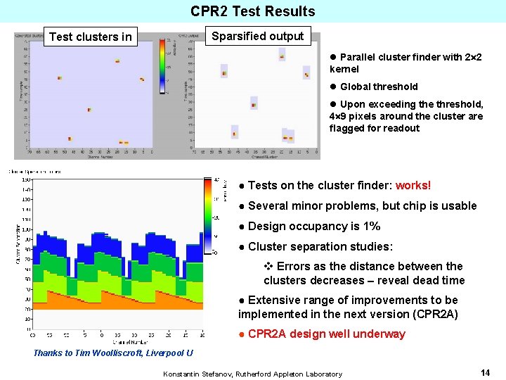
CPR 2 Test Results Sparsified output Test clusters in l Parallel cluster finder with 2 2 kernel l Global threshold l Upon exceeding the threshold, 4 9 pixels around the cluster are flagged for readout ● Tests on the cluster finder: works! ● Several minor problems, but chip is usable ● Design occupancy is 1% ● Cluster separation studies: v Errors as the distance between the clusters decreases – reveal dead time ● Extensive range of improvements to be implemented in the next version (CPR 2 A) ● CPR 2 A design well underway Thanks to Tim Woolliscroft, Liverpool U Konstantin Stefanov, Rutherford Appleton Laboratory 14
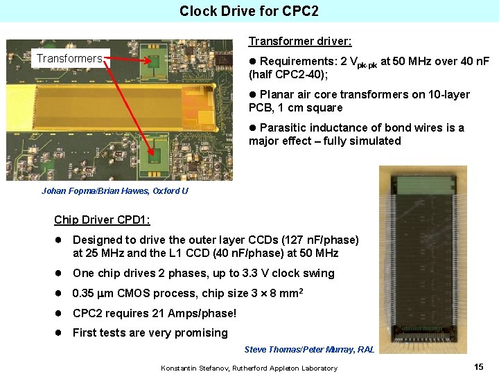
Clock Drive for CPC 2 Transformer driver: Transformers l Requirements: 2 Vpk-pk at 50 MHz over 40 n. F (half CPC 2 -40); l Planar air core transformers on 10 -layer PCB, 1 cm square l Parasitic inductance of bond wires is a major effect – fully simulated Johan Fopma/Brian Hawes, Oxford U Chip Driver CPD 1: ● Designed to drive the outer layer CCDs (127 n. F/phase) at 25 MHz and the L 1 CCD (40 n. F/phase) at 50 MHz ● ● One chip drives 2 phases, up to 3. 3 V clock swing 0. 35 m CMOS process, chip size 3 8 mm 2 CPC 2 requires 21 Amps/phase! First tests are very promising Steve Thomas/Peter Murray, RAL Konstantin Stefanov, Rutherford Appleton Laboratory 15
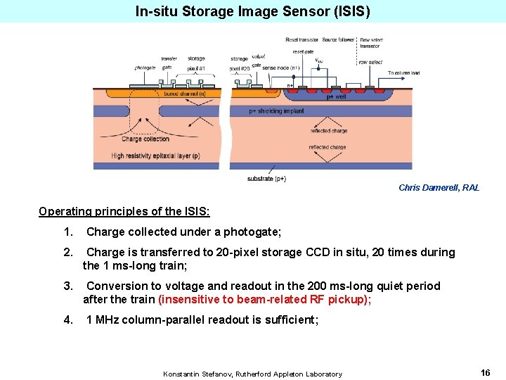
In-situ Storage Image Sensor (ISIS) Chris Damerell, RAL Operating principles of the ISIS: 1. Charge collected under a photogate; 2. Charge is transferred to 20 -pixel storage CCD in situ, 20 times during the 1 ms-long train; 3. Conversion to voltage and readout in the 200 ms-long quiet period after the train (insensitive to beam-related RF pickup); 4. 1 MHz column-parallel readout is sufficient; Konstantin Stefanov, Rutherford Appleton Laboratory 16
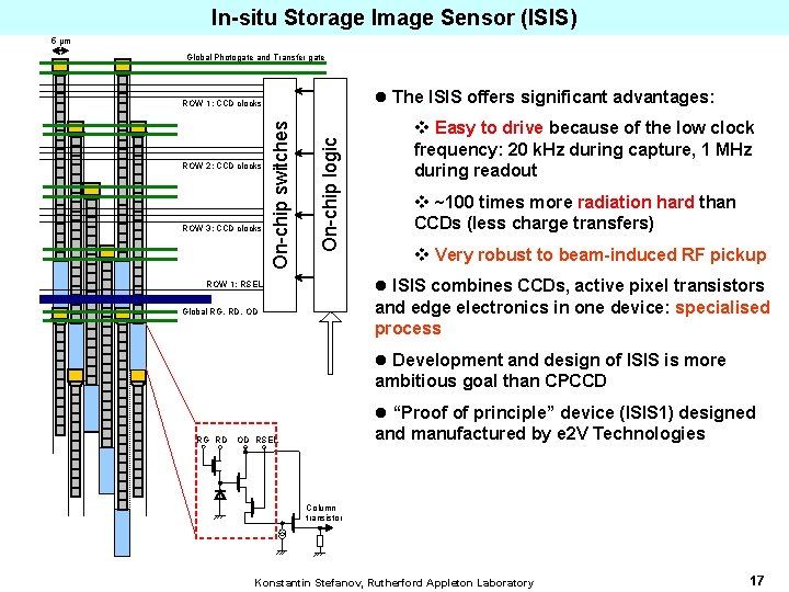
In-situ Storage Image Sensor (ISIS) 5 μm Global Photogate and Transfer gate l The ISIS offers significant advantages: ROW 3: CCD clocks On-chip logic ROW 2: CCD clocks On-chip switches ROW 1: CCD clocks v Easy to drive because of the low clock frequency: 20 k. Hz during capture, 1 MHz during readout v ~100 times more radiation hard than CCDs (less charge transfers) v Very robust to beam-induced RF pickup l ISIS combines CCDs, active pixel transistors and edge electronics in one device: specialised process ROW 1: RSEL Global RG, RD, OD l Development and design of ISIS is more ambitious goal than CPCCD RG RD l “Proof of principle” device (ISIS 1) designed and manufactured by e 2 V Technologies OD RSEL Column transistor Konstantin Stefanov, Rutherford Appleton Laboratory 17
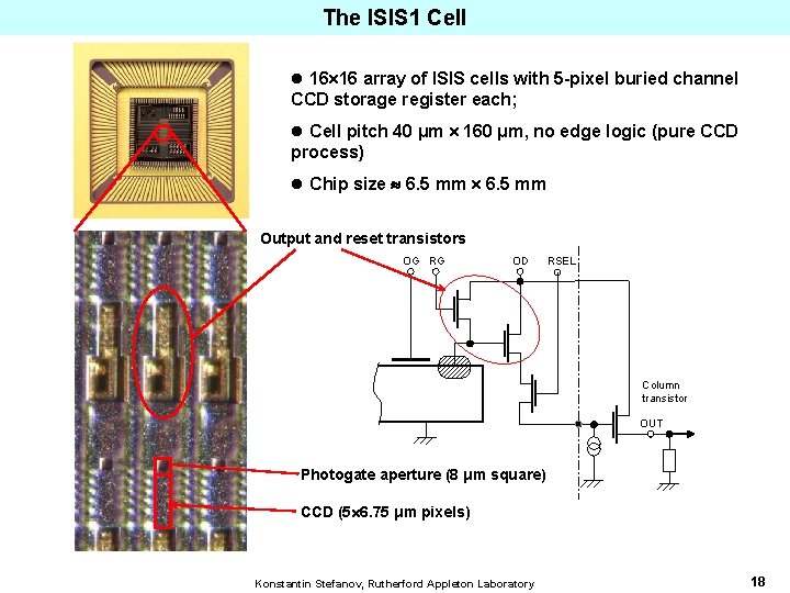
The ISIS 1 Cell l 16 16 array of ISIS cells with 5 -pixel buried channel CCD storage register each; l Cell pitch 40 μm 160 μm, no edge logic (pure CCD process) l Chip size 6. 5 mm Output and reset transistors OG RG OD RSEL Column transistor OUT Photogate aperture (8 μm square) CCD (5 6. 75 μm pixels) Konstantin Stefanov, Rutherford Appleton Laboratory 18
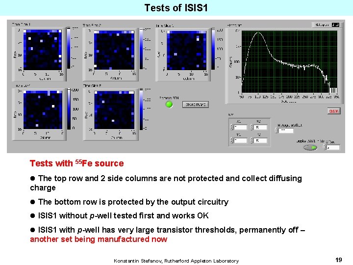
Tests of ISIS 1 Tests with 55 Fe source l The top row and 2 side columns are not protected and collect diffusing charge l The bottom row is protected by the output circuitry l ISIS 1 without p-well tested first and works OK l ISIS 1 with p-well has very large transistor thresholds, permanently off – another set being manufactured now Konstantin Stefanov, Rutherford Appleton Laboratory 19
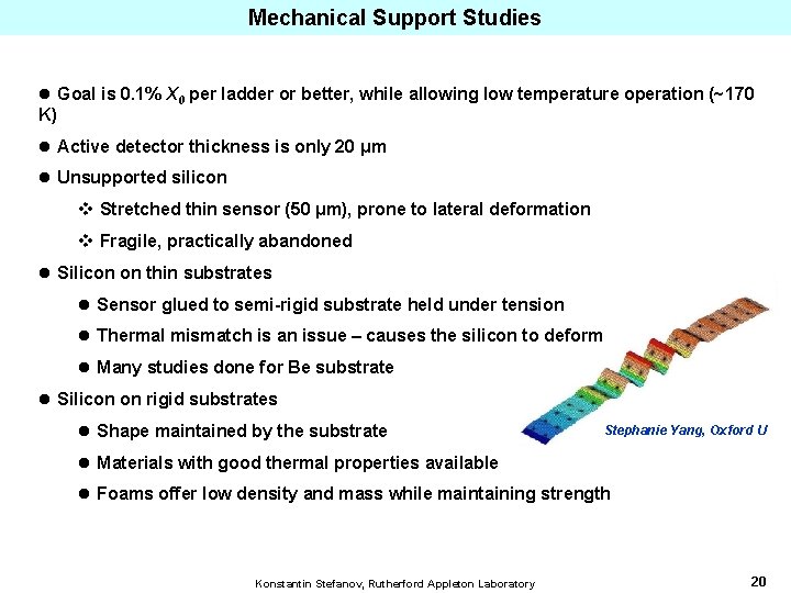
Mechanical Support Studies l Goal is 0. 1% X 0 per ladder or better, while allowing low temperature operation (~170 K) l Active detector thickness is only 20 μm l Unsupported silicon v Stretched thin sensor (50 μm), prone to lateral deformation v Fragile, practically abandoned l Silicon on thin substrates l Sensor glued to semi-rigid substrate held under tension l Thermal mismatch is an issue – causes the silicon to deform l Many studies done for Be substrate l Silicon on rigid substrates l Shape maintained by the substrate Stephanie Yang, Oxford U l Materials with good thermal properties available l Foams offer low density and mass while maintaining strength Konstantin Stefanov, Rutherford Appleton Laboratory 20
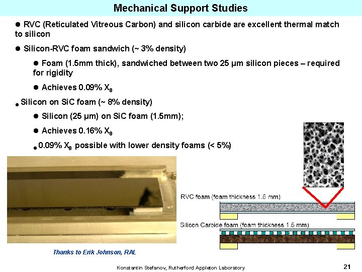
Mechanical Support Studies l RVC (Reticulated Vitreous Carbon) and silicon carbide are excellent thermal match to silicon l Silicon-RVC foam sandwich (~ 3% density) l Foam (1. 5 mm thick), sandwiched between two 25 μm silicon pieces – required for rigidity l Achieves 0. 09% X 0 l Silicon on Si. C foam (~ 8% density) l Silicon (25 μm) on Si. C foam (1. 5 mm); l Achieves 0. 16% X 0 l 0. 09% X 0 possible with lower density foams (< 5%) Thanks to Erik Johnson, RAL Konstantin Stefanov, Rutherford Appleton Laboratory 21
Areas of Common Interest for LCFI and CALICE (personal opinion) l Detector simulations v Vertex package – provides important building block for full detector simulation and performance checks against benchmark physics processes l Detector tests v Laser system at RAL could be used for both MAPS and CCD/ISIS test l Detector design v Pulsed power – storage supercapacitors considered for LCFI l Beam tests v Combined beam tests in the future welcome v Some overlap in the electronics may be possible v Presently resources for beam tests at LCFI are limited v Could conduct first beam tests on CPC 2 this year if all goes well Konstantin Stefanov, Rutherford Appleton Laboratory 22
Conclusions l Vertex package near release v Major milestone for LCFI, huge amount of work by a small team v Will provide important contribution to the MARLIN event reconstruction framework v Eagerly anticipated worldwide l Detector R&D program progressing well: v Second generation CPCCD and readout chip being evaluated v Driver system using CMOS chip and transformers under development v Third generation CMOS readout chips for CPC 1/2 in design stage v Design of second generation, small pixel ISIS 2 underway l Mechanical support aims at 0. 1% X 0 using modern materials l Several areas of collaboration between CALICE and LCFI possible Konstantin Stefanov, Rutherford Appleton Laboratory 23
- Slides: 23