LAYER FILMS APPLIED TO SRF AnneMarie VALENTEFELICIANO On

- Slides: 11

LAYER FILMS APPLIED TO SRF Anne-Marie VALENTE-FELICIANO On behalf of the HEPTHF Collaboration

SRF Thin Films Collaboration Films creation: Jlab: A-M Valente-Feliciano, J. Spradlin, L. Phillips W&M: A. Lukaszew, D. Beringer Material and RF characterization: Jlab: A-M Valente-Feliciano, J. Spradlin, L. Phillips, X. Zhao, B. Xiao, A. Wu W&M: A. Lukaszew, D. Beringer, S. , R. Outlaw, O. Trofinova NSU: K. Seo ODU: H. Baumgart, D. Gu Black Labs LLC: R. Crooks Under DOE HEP Grant ARRA & U. S. DOE Contract No. DE-AC 05 -06 OR 23177

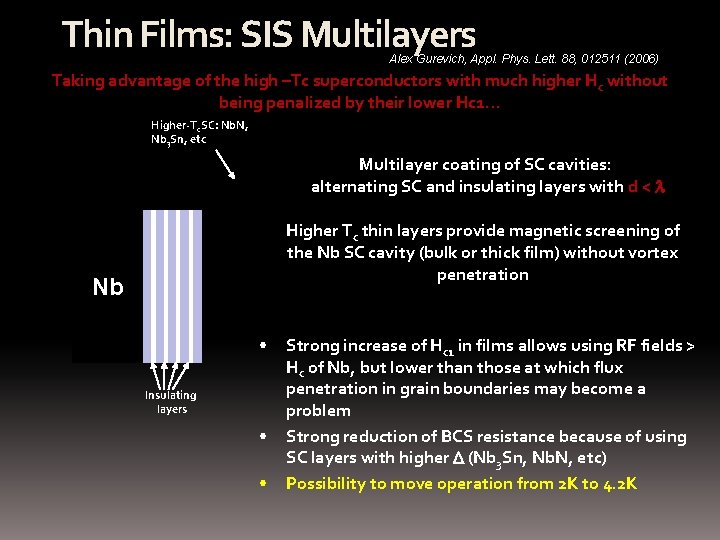
Thin Films: SIS Multilayers Alex Gurevich, Appl. Phys. Lett. 88, 012511 (2006) Taking advantage of the high –Tc superconductors with much higher Hc without being penalized by their lower Hc 1… Higher-Tc. SC: Nb. N, Nb 3 Sn, etc Multilayer coating of SC cavities: alternating SC and insulating layers with d < Higher Tc thin layers provide magnetic screening of the Nb SC cavity (bulk or thick film) without vortex penetration Nb • Insulating layers • • Strong increase of Hc 1 in films allows using RF fields > Hc of Nb, but lower than those at which flux penetration in grain boundaries may become a problem Strong reduction of BCS resistance because of using SC layers with higher (Nb 3 Sn, Nb. N, etc) Possibility to move operation from 2 K to 4. 2 K

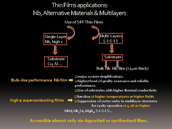
Thin Films applications: Nb, Alternative Materials & Multilayers Use of SRF Thin Films Single Layer Nb, high k Substrate Cu, Al … Bulk-like performance Nb film Multi-Layers S-I-S Substrate Bulk Nb Nb film (>1 mm thick) qmajor system simplifications. qhighest level of quality assurance and reliable performance. q. Use of substrates with higher thermal conductivity high k superconducting films qfunction at higher temperatures or higher fields q. Suppression of vortex entry in multilayer structures for cavity operation at 4. 2 K or higher Nb. N, Nb 3 Sn, Mg. B 2, S-I-S… Accessible almost only via deposited or synthesized films.

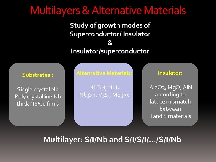
Approach SIS Multilayer Structures: üNucleation studies of Nb. Ti. N, Nb. N on dielectrics like Mg. O, Al 2 O 3 and reciprocately. üCreation and characterization of a set of Nb. Ti. N , Nb. N…/insulator/Nb samples by UHV multi-target energetic ion deposition with well-controlled, incremented thickness. The variation of rf field properties with temperature as a function of thickness of the superconducting overlayer will provide a direct test of the Gurevich delayed flux entry model.

Tailoring for optimum RF performance Careful characterization of the attained composition and microstructure Close association with resulting rf surface impedance and superconducting properties

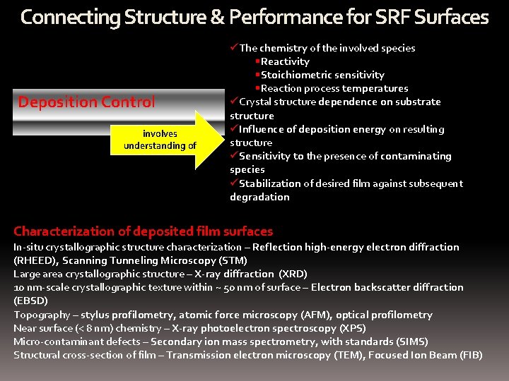
Connecting Structure & Performance for SRF Surfaces Deposition Control involves understanding of üThe chemistry of the involved species §Reactivity §Stoichiometric sensitivity §Reaction process temperatures üCrystal structure dependence on substrate structure üInfluence of deposition energy on resulting structure üSensitivity to the presence of contaminating species üStabilization of desired film against subsequent degradation Characterization of deposited film surfaces In-situ crystallographic structure characterization – Reflection high-energy electron diffraction (RHEED), Scanning Tunneling Microscopy (STM) Large area crystallographic structure – X-ray diffraction (XRD) 10 nm-scale crystallographic texture within ~ 50 nm of surface – Electron backscatter diffraction (EBSD) Topography – stylus profilometry, atomic force microscopy (AFM), optical profilometry Near surface (< 8 nm) chemistry – X-ray photoelectron spectroscopy (XPS) Micro-contaminant defects – Secondary ion mass spectrometry, with standards (SIMS) Structural cross-section of film – Transmission electron microscopy (TEM), Focused Ion Beam (FIB)

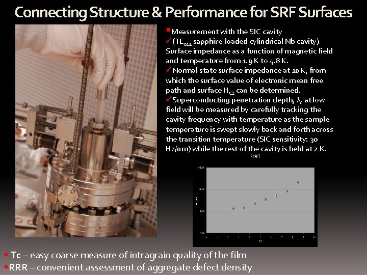
Connecting Structure & Performance for SRF Surfaces §Measurement with the SIC cavity MATERIAL PROPERTIES ü(TE 011 sapphire-loaded cylindrical Nb cavity) Surface impedance as a function of magnetic field and temperature from 1. 9 K to 4. 8 K. üNormal state surface impedance at 10 K, from which the surface value of electronic mean free path and surface Hc 1 can be determined. üSuperconducting penetration depth, λ, at low field will be measured by carefully tracking the cavity frequency with temperature as the sample temperature is swept slowly back and forth across the transition temperature (SIC sensitivity: 30 Hz/nm) while the rest of the cavity is held at 2 K. § Tc – easy coarse measure of intragrain quality of the film §RRR – convenient assessment of aggregate defect density

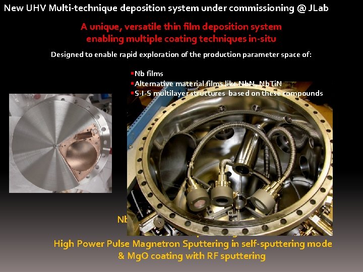
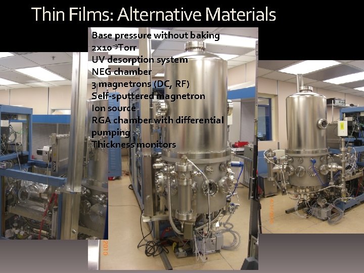
New UHV Multi-technique deposition system under commissioning @ JLab A unique, versatile thin film deposition system enabling multiple coating techniques in-situ Designed to enable rapid exploration of the production parameter space of: §Nb films §Alternative material films like Nb. N, Nb. Ti. N §S-I-S multilayer structures based on these compounds Nb. Ti. N, Nb. N, Mo 3 Re, V 3 Si coatings with Reactive Sputtering and High Power Pulse Magnetron Sputtering in self-sputtering mode & Mg. O coating with RF sputtering

Thin Films: Alternative Materials Substrates Base pressure without baking 2 x 10 -9 Torr UV desorption system NEG chamber 3 magnetrons (DC, RF) Self-sputtered magnetron Ion source RGA chamber with differential pumping Thickness monitors

Multilayers & Alternative Materials Study of growth modes of Superconductor/ Insulator & Insulator/superconductor Substrates : Alternative Materials: Insulator: Single crystal Nb Poly crystalline Nb thick Nb/Cu films Nb. Ti. N, Nb. N Nb 3 Sn, V 3 Si, Mo 3 Re Al 2 O 3, Mg. O, Al. N according to lattice mismatch between I and S materials Multilayer: S/I/Nb and S/I/…/S/I/Nb