LATEST ANALOG MEMORY DEVELOPMENTS AT IRFU THE SAMPIC


- Slides: 41

LATEST ANALOG MEMORY DEVELOPMENTS AT IRFU: THE SAMPIC WTDC CHIP O. Gevin 1 E. Delagnes 1 H. Grabas 1 D. Breton 2 J. Maalmi 2 SAMpler for PICosecond time pick off 1 CEA/IRFU Saclay 2 CNRS/IN 2 P 3/LAL Orsay This work has been funded by the P 2 IO Lab. Ex (ANR 10 -LABX-0038) in the framework « Investissements d’Avenir » (ANR-11 -IDEX-0003 -01) managed by the French National Research Agency (ANR). FEE 2014, Argonne NL. 1 olivier. gevin@cea. fr, eric. delagnes@cea. fr

INTRODUCTION § Test chip = common prototype before designing specific chips for ATLAS AFP and Super. B TOF § R&D funded by “P 2 IO” grant (not by experiments) § Goals for the first prototype: § Evaluation of AMS 0. 18µm technology § Evaluate new design options (DLL & SCA) § Evaluate simultaneous R/W § Multichannel Chip usable in a real environment (with detector and a real DAQ) FEE 2014, Argonne NL. | PAGE 2

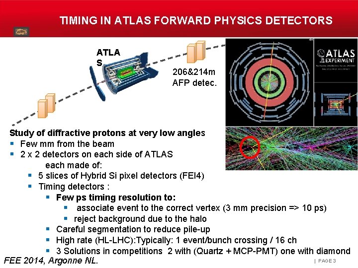
TIMING IN ATLAS FORWARD PHYSICS DETECTORS ATLA S 206&214 m AFP detec. Study of diffractive protons at very low angles § Few mm from the beam § 2 x 2 detectors on each side of ATLAS each made of: § 5 slices of Hybrid Si pixel detectors (FEI 4) § Timing detectors : § Few ps timing resolution to: § associate event to the correct vertex (3 mm precision => 10 ps) § reject background due to the halo § Careful segmentation to reduce pile-up § High rate (HL-LHC): Typically: 1 event/bunch crossing / 16 ch § 3 Solutions in competitions 2 with (Quartz + MCP-PMT) one with diamond | PAGE 3 FEE 2014, Argonne NL.

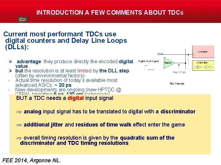
INTRODUCTION A FEW COMMENTS ABOUT TDCs Current most performant TDCs use digital counters and Delay Line Loops (DLLs): Ø advantage: they produce directly the encoded digital value Ø but the resolution is at least limited by the DLL step (often by environmental factors) - Actual time resolution of today’s available most advanced ASICs: ~ 20 ps - New developments are ongoing (new HPTDC @ CERN, targetting 5 ps, 130 nm technology) BUT a TDC needs a digital input signal Þ analog input signal has to be translated to digital with a discriminator Þ additional jitter and residues of time walk effect enter the game Þ overall timing resolution is given by the quadratic sum of the discriminator and TDC timing resolutions FEE 2014, Argonne NL.

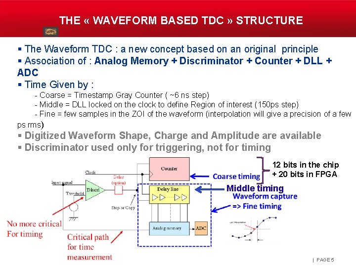
THE « WAVEFORM BASED TDC » STRUCTURE § The Waveform TDC : a new concept based on an original principle § Association of : Analog Memory + Discriminator + Counter + DLL + ADC § Time Given by : - Coarse = Timestamp Gray Counter ( ~6 ns step) - Middle = DLL locked on the clock to define Region of interest (150 ps step) - Fine = few samples in the ZOI of the waveform (interpolation will give a precision of a few ps rms) § Digitized Waveform Shape, Charge and Amplitude are available § Discriminator used only for triggering, not for timing 12 bits in the chip + 20 bits in FPGA Middle timing | PAGE 5

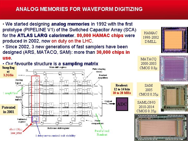
ANALOG MEMORIES FOR WAVEFORM DIGITIZING • We started designing analog memories in 1992 with the first prototype (PIPELINE V 1) of the Switched Capacitor Array (SCA) for the ATLAS LARG calorimeter. 80, 000 HAMAC chips were produced in 2002, now on duty on the LHC. • Since 2002, 3 new generations of fast samplers have been designed (ARS, MATACQ, SAM): more than 30, 000 chips in use. • Our favourite structure is a sampling matrix Sampling at 3. 2 GS/s Readout: 12 to 14 bits 10 to 20 MHz Patented in 2001 ADC HAMAC 1998 -2002 DMILL MATACQ 2000 -2003 CMOS 0. 8µ SAM 2005 CMOS 0. 35µ SAMLONG 2010 -2014 CMOS 0. 35µ PAGE 6

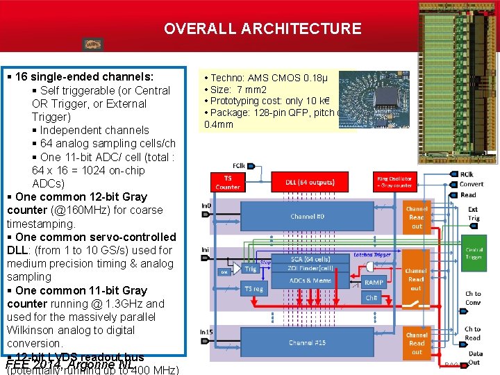
OVERALL ARCHITECTURE § 16 single-ended channels: § Self triggerable (or Central OR Trigger, or External Trigger) § Independent channels § 64 analog sampling cells/ch § One 11 -bit ADC/ cell (total : 64 x 16 = 1024 on-chip ADCs) § One common 12 -bit Gray counter (@160 MHz) for coarse timestamping. § One common servo-controlled DLL: (from 1 to 10 GS/s) used for medium precision timing & analog sampling § One common 11 -bit Gray counter running @ 1. 3 GHz and used for the massively parallel Wilkinson analog to digital conversion. § 12 -bit LVDS readout bus FEE 2014, Argonne NL. (potentially running up to 400 MHz) • Techno: AMS CMOS 0. 18µ • Size: 7 mm 2 • Prototyping cost: only 10 k€ • Package: 128 -pin QFP, pitch of 0. 4 mm | PAGE 7

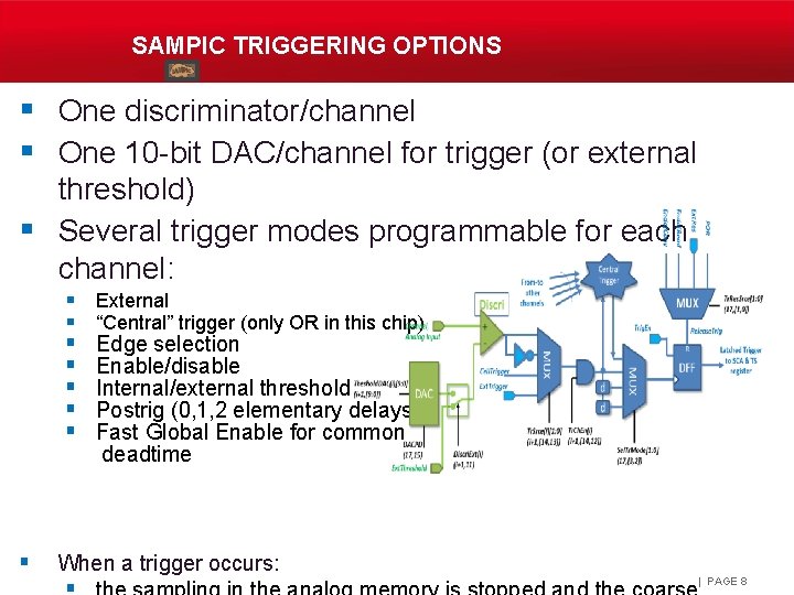
SAMPIC TRIGGERING OPTIONS § One discriminator/channel § One 10 -bit DAC/channel for trigger (or external threshold) § Several trigger modes programmable for each channel: § External § “Central” trigger (only OR in this chip) § Edge selection § Enable/disable § Internal/external threshold § Postrig (0, 1, 2 elementary delays) § Fast Global Enable for common deadtime § When a trigger occurs: | PAGE 8

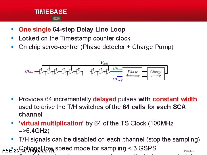
TIMEBASE § One single 64 -step Delay Line Loop § Locked on the Timestamp counter clock § On chip servo-control (Phase detector + Charge Pump) § Provides 64 incrementally delayed pulses with constant width used to drive the T/H switches of the 64 cells for each SCA channel § ‘virtual multiplication’ by 64 of the TS Clock (100 MHz =>6. 4 GHz) § T/H signals can be disabled on each channel (stop the sampling) § Optional low speed mode for sampling < 3 GSPS | PAGE 9 FEE 2014, Argonne NL.

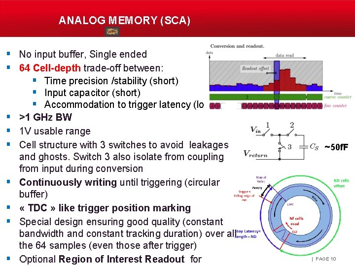
ANALOG MEMORY (SCA) § No input buffer, Single ended § 64 Cell-depth trade-off between: § Time precision /stability (short) § Input capacitor (short) § Accommodation to trigger latency (long) § >1 GHz BW § 1 V usable range § Cell structure with 3 switches to avoid leakages § § and ghosts. Switch 3 also isolate from coupling from input during conversion Continuously writing until triggering (circular buffer) « TDC » like trigger position marking Special design ensuring good quality (constant bandwidth and constant tracking duration) over all the 64 samples (even those after trigger) Optional Region of Interest Readout for ~50 f. F | PAGE 10

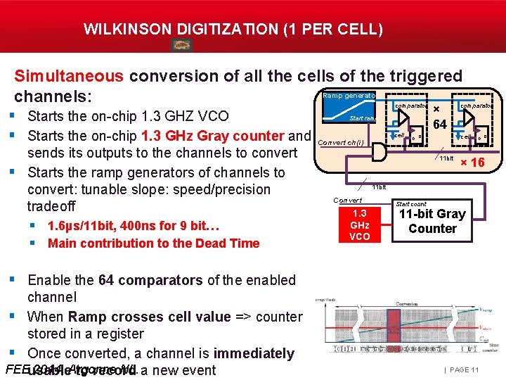
WILKINSON DIGITIZATION (1 PER CELL) Simultaneous conversion of all the cells of the triggered Ramp generator channels: comparator § Starts the on-chip 1. 3 GHZ VCO § Starts the on-chip 1. 3 GHz Gray counter and Convert ch(i) Start ramp sends its outputs to the channels to convert § Starts the ramp generators of channels to convert: tunable slope: speed/precision tradeoff § 1. 6µs/11 bit, 400 ns for 9 bit… § Main contribution to the Dead Time cell × 64 comparator cell D Q 11 bit D Q × 16 11 bit Convert 1. 3 GHz VCO Start count 11 -bit Gray Counter § Enable the 64 comparators of the enabled channel § When Ramp crosses cell value => counter stored in a register § Once converted, a channel is immediately FEE 2014, Argonne NL. usable to record a new event | PAGE 11

READOUT § Readout (Read and RCk signals) § Data read channel by channel § Rotating priority mechanism to avoid reading always the same channel § Region of interest readout to reduce the deadtime (nb of cell read can be chosen dynamically) § Readout of the converted data through a 12 -bit LVDS bus: § Timestamps § Trigger Cell Index § Channel Identifier § The cells (all or a selected set) of a given channel are read sequentially § Up to 4. 8 Gbit/s § Channel is not in deadtime during Readout (the data register is really a buffer stage) | PAGE 12

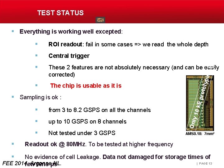
TEST STATUS § Everything is working well excepted: ROI readout: fail in some cases => we read the whole depth § Central trigger § These 2 features are not absolutely necessary (and can be easily corrected) § The chip is usable as it is § § from 3 to 8. 2 GSPS on all the channels § up to 10 GSPS on 8 channels § Not tested under 3 GSPS 10 k § Only § Sampling is ok : E pr otot ypin g !!! § AMS 0. 18: 7 mm 2 Readout ok @ 80 MHz. To be tested at higher frequency No evidence of cell Leakage. Data not damaged for storage times of | PAGE 13 FEE 2014, Argonne NL. few tens µs

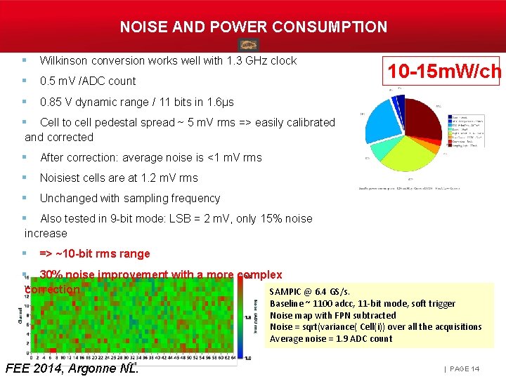
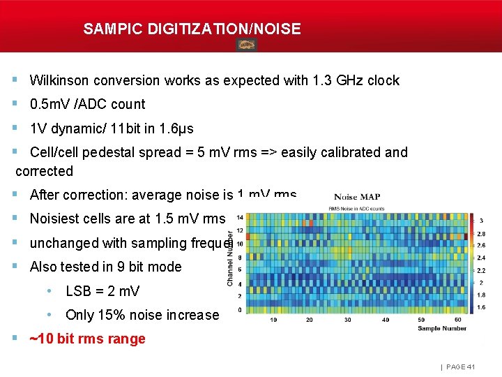
NOISE AND POWER CONSUMPTION § Wilkinson conversion works well with 1. 3 GHz clock § 0. 5 m. V /ADC count § 0. 85 V dynamic range / 11 bits in 1. 6µs 10 -15 m. W/ch § Cell to cell pedestal spread ~ 5 m. V rms => easily calibrated and corrected § After correction: average noise is <1 m. V rms § Noisiest cells are at 1. 2 m. V rms § Unchanged with sampling frequency § Also tested in 9 -bit mode: LSB = 2 m. V, only 15% noise increase § => ~10 -bit rms range § 30% noise improvement with a more complex correction SAMPIC @ 6. 4 GS/s. Baseline ~ 1100 adcc, 11 -bit mode, soft trigger Noise map with FPN subtracted Noise = sqrt(variance( Cell(i)) over all the acquisitions Average noise = 1. 9 ADC count FEE 2014, Argonne NL. | PAGE 14

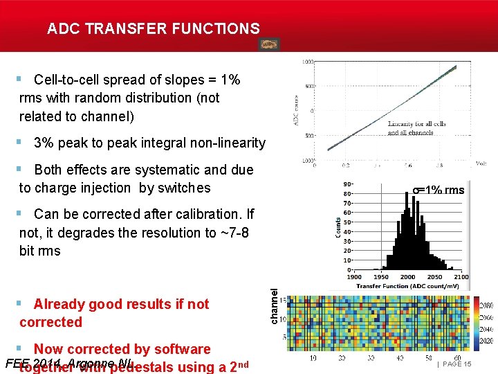
ADC TRANSFER FUNCTIONS § Cell-to-cell spread of slopes = 1% rms with random distribution (not related to channel) § 3% peak to peak integral non-linearity BANDWIDTH & TRIGGER s=1% rms § Both effects are systematic and due to charge injection by switches § Can be corrected after calibration. If § Already good results if not corrected channel not, it degrades the resolution to ~7 -8 bit rms § Now corrected by software FEE 2014, Argonne NL. together with pedestals using a 2 nd | PAGE 15

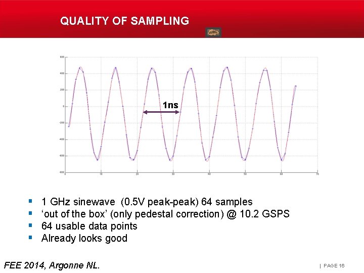
QUALITY OF SAMPLING 1 ns § § 1 GHz sinewave (0. 5 V peak-peak) 64 samples ‘out of the box’ (only pedestal correction) @ 10. 2 GSPS 64 usable data points Already looks good FEE 2014, Argonne NL. | PAGE 16

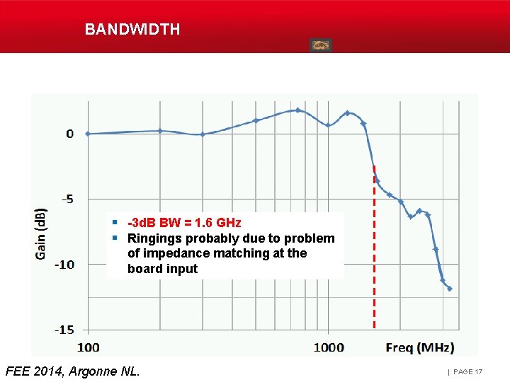
BANDWIDTH § -3 d. B BW = 1. 6 GHz § Ringings probably due to problem of impedance matching at the board input FEE 2014, Argonne NL. | PAGE 17

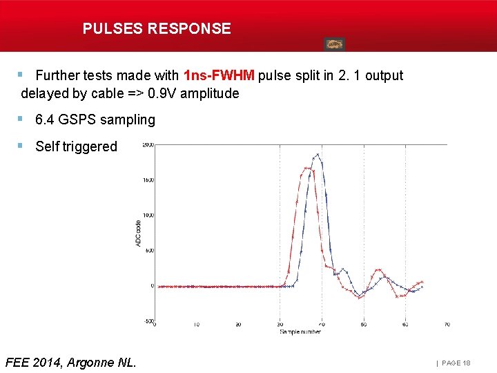
PULSES RESPONSE § Further tests made with 1 ns-FWHM pulse split in 2. 1 output delayed by cable => 0. 9 V amplitude § 6. 4 GSPS sampling § Self triggered FEE 2014, Argonne NL. | PAGE 18

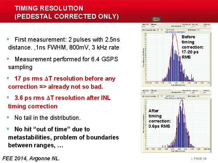
TIMING RESOLUTION (PEDESTAL CORRECTED ONLY) Before timing correction: 17 -20 ps RMS § First measurement: 2 pulses with 2. 5 ns distance. , 1 ns FWHM, 800 m. V, 3 k. Hz rate § Measurement performed for 6. 4 GSPS sampling § 17 ps rms ΔT resolution before any correction => already not so bad. § 3. 6 ps rms ΔT resolution after INL timing correction § No tail in the distribution. § No hit “out of time” due to After timing correction: 3. 6 ps RMS metastabilities, problem of boundaries between ranges, … FEE 2014, Argonne NL. | PAGE 19

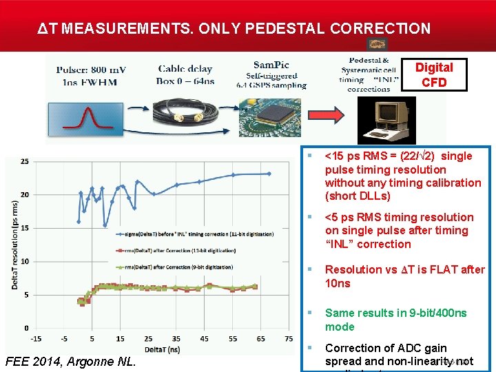
ΔT MEASUREMENTS. ONLY PEDESTAL CORRECTION Digital CFD FEE 2014, Argonne NL. § <15 ps RMS = (22/√ 2) single pulse timing resolution without any timing calibration (short DLLs) § <5 ps RMS timing resolution on single pulse after timing “INL” correction § Resolution vs ΔT is FLAT after 10 ns § Same results in 9 -bit/400 ns mode § Correction of ADC gain | PAGE 20 spread and non-linearity not

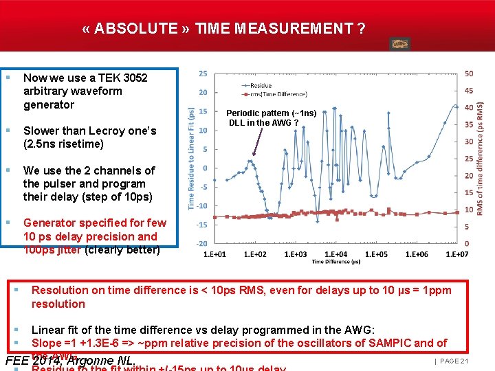
« ABSOLUTE » TIME MEASUREMENT ? § Now we use a TEK 3052 arbitrary waveform generator § Slower than Lecroy one’s (2. 5 ns risetime) § We use the 2 channels of the pulser and program their delay (step of 10 ps) § Generator specified for few 10 ps delay precision and 100 ps jitter (clearly better) § Periodic pattern (~1 ns) DLL in the AWG ? Resolution on time difference is < 10 ps RMS, even for delays up to 10 µs = 1 ppm resolution § Linear fit of the time difference vs delay programmed in the AWG: § Slope =1 +1. 3 E-6 => ~ppm relative precision of the oscillators of SAMPIC and of the AWG | PAGE 21 FEE 2014, Argonne NL.

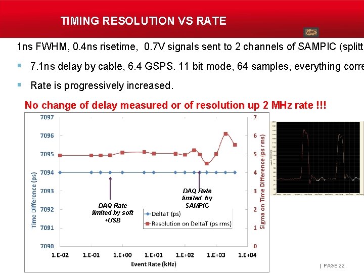
TIMING RESOLUTION VS RATE 1 ns FWHM, 0. 4 ns risetime, 0. 7 V signals sent to 2 channels of SAMPIC (splitte § 7. 1 ns delay by cable, 6. 4 GSPS. 11 bit mode, 64 samples, everything corre § Rate is progressively increased. No change of delay measured or of resolution up 2 MHz rate !!! DAQ Rate limited by soft +USB DAQ Rate limited by SAMPIC | PAGE 22

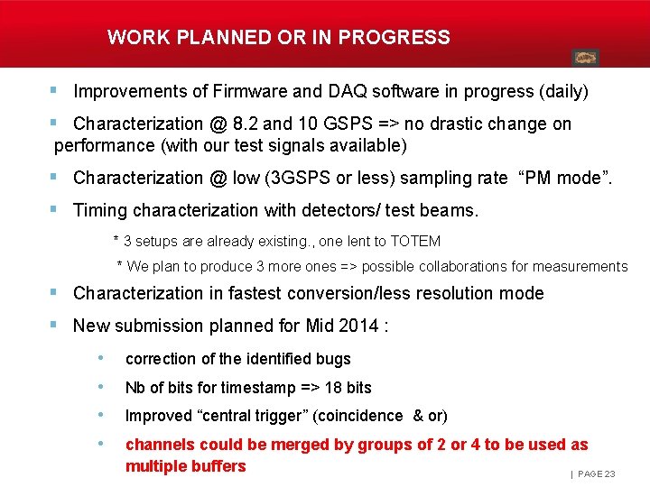
WORK PLANNED OR IN PROGRESS § Improvements of Firmware and DAQ software in progress (daily) § Characterization @ 8. 2 and 10 GSPS => no drastic change on performance (with our test signals available) § Characterization @ low (3 GSPS or less) sampling rate “PM mode”. § Timing characterization with detectors/ test beams. * 3 setups are already existing. , one lent to TOTEM * We plan to produce 3 more ones => possible collaborations for measurements § Characterization in fastest conversion/less resolution mode § New submission planned for Mid 2014 : • correction of the identified bugs • Nb of bits for timestamp => 18 bits • Improved “central trigger” (coincidence & or) • channels could be merged by groups of 2 or 4 to be used as multiple buffers | PAGE 23

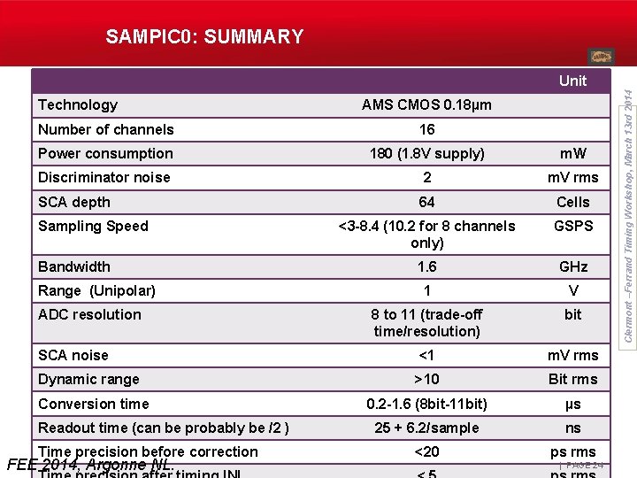
SAMPIC 0: SUMMARY Technology AMS CMOS 0. 18µm Number of channels 16 Power consumption 180 (1. 8 V supply) m. W Discriminator noise 2 m. V rms SCA depth 64 Cells <3 -8. 4 (10. 2 for 8 channels only) GSPS 1. 6 GHz 1 V 8 to 11 (trade-off time/resolution) bit SCA noise <1 m. V rms Dynamic range >10 Bit rms 0. 2 -1. 6 (8 bit-11 bit) µs 25 + 6. 2/sample ns <20 ps rms Sampling Speed Bandwidth Range (Unipolar) ADC resolution Conversion time Readout time (can be probably be /2 ) Time precision before correction FEE 2014, Argonne NL. | PAGE 24 Clermont –Ferrand Timing Workshop, March 13 rd 2014 Unit

CONCLUSION A self-triggered WTDC chip demonstrator has been designed and characterized: § Works well with expected performance: § 1. 6 GHz BW § up to 10 GSPS § Low noise (trigger and acquisition) § < 5 ps rms timing resolution § Already meets our initial requirements § Already usable for tests with detectors § Work ongoing on: § DAQ System (firmware + software) optimization § Existing chip fine characterization § Second prototype THANK YOU FOR YOUR ATTENTION FEE 2014, Argonne NL. | PAGE 25

BACKUP SLIDES | PAGE 26

§ Based on IBM 0. 18µm : IBM quality & documentation § Good Standard Cells Library § Good lifetime foreseen (HV module, automotive) § 1. 8 V power supply: nice for analog design/ high dynamic range § Reasonable leakages § Good noise properties ( already checked with Idef. X chips for Cd. Te) § Reasonable radiation hardness § Less complex (and less expensive) than IBM 0. 13µm § AMS high quality Design Kit § Easy access (CMP, Europractice, AMS) Clermont –Ferrand Timing Workshop, March 13 rd 2014 WHY AMS 0. 18Μ ?

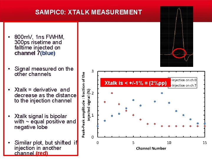
SAMPIC 0: XTALK MEASUREMENT • 800 m. V, 1 ns FWHM, 300 ps risetime and falltime injected on channel 7(blue) • Signal measured on the other channels Xtalk is < +/-1% = (2%pp) • Xtalk = derivative and decrease as the distance to the injection channel • Xtalk signal is bipolar with ~ equal positive and negative lobe • Similar plot, but shifted if injection in another channel (red)

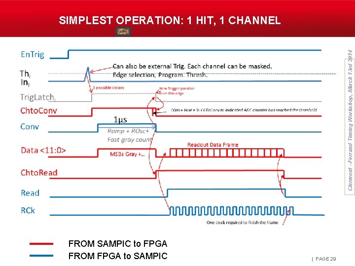
Clermont –Ferrand Timing Workshop, March 13 rd 2014 SIMPLEST OPERATION: 1 HIT, 1 CHANNEL FROM SAMPIC to FPGA FROM FPGA to SAMPIC | PAGE 29

MULTIPLE HITS, 1 CHANNEL | PAGE 30

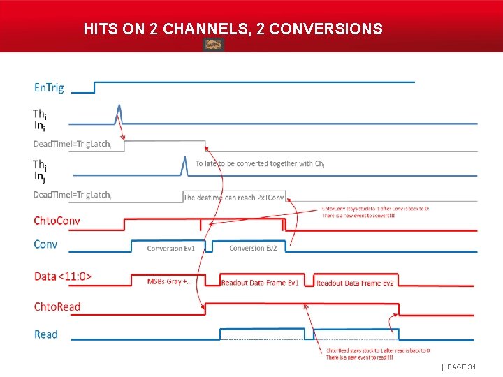
HITS ON 2 CHANNELS, 2 CONVERSIONS | PAGE 31

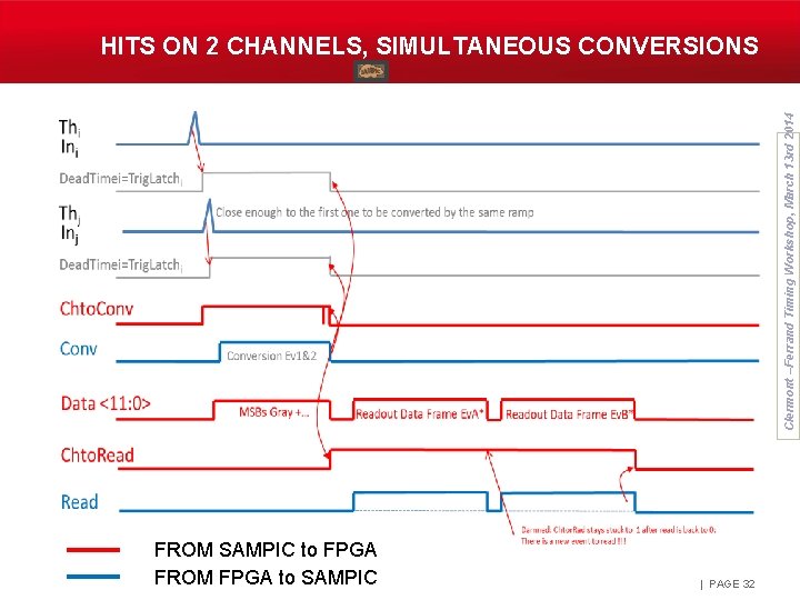
Clermont –Ferrand Timing Workshop, March 13 rd 2014 HITS ON 2 CHANNELS, SIMULTANEOUS CONVERSIONS FROM SAMPIC to FPGA FROM FPGA to SAMPIC | PAGE 32

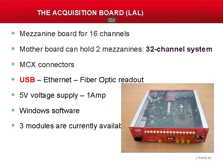
THE ACQUISITION BOARD (LAL) § Mezzanine board for 16 channels § Mother board can hold 2 mezzanines: 32 -channel system § MCX connectors § USB – Ethernet – Fiber Optic readout § 5 V voltage supply – 1 Amp § Windows software § 3 modules are currently available THE BOARD | PAGE 33

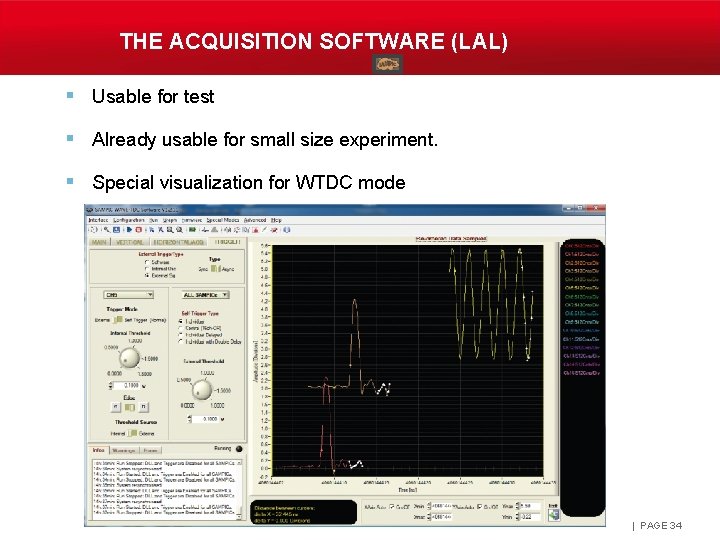
THE ACQUISITION SOFTWARE (LAL) § Usable for test § Already usable for small size experiment. § Special visualization for WTDC mode PREREQUISIT ES | PAGE 34

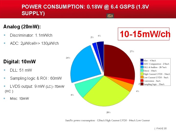
POWER CONSUMPTION: 0. 18 W @ 6. 4 GSPS (1. 8 V SUPPLY) Analog (20 m. W): § Discriminator: 1. 1 m. W/ch § ADC: 2µW/cell=> 130µW/ch 10 -15 m. W/ch Digital: 10 m. W § DLL: 51 m. W § Sampling logic & ROI : 60 m. W § LVDS output: 9 m. W (LC) -70 m. W (HC ) § Misc: 10 m. W | PAGE 35

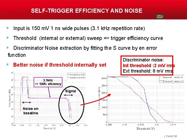
SELF-TRIGGER EFFICIENCY AND NOISE § Input is 150 m. V 1 ns wide pulses (3. 1 k. Hz repetition rate) § Threshold (internal or external) sweep => trigger efficiency curve § Discriminator Noise extraction by fitting the S curve by en error function § Better noise if threshold internally set Discriminator noise: Int threshold : 2 m. V rms Ext threshold: 8 m. V rms 3. 1 k. Hz => 100% eficiency Signal Noise on baseline | PAGE 36

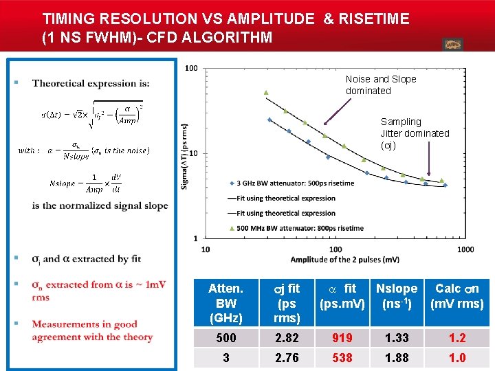
TIMING RESOLUTION VS AMPLITUDE & RISETIME (1 NS FWHM)- CFD ALGORITHM Noise and Slope dominated Sampling Jitter dominated (sj) a fit Nslope Calc sn (ps. m. V) (ns-1) (m. V rms) Atten. BW (GHz) sj fit (ps rms) 500 2. 82 919 1. 33 3 2. 76 538 1. 88 1. 2 1. 0 | PAGE 37

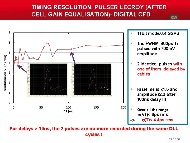
TIMING RESOLUTION, PULSER LECROY (AFTER CELL GAIN EQUALISATION)- DIGITAL CFD § 11 bit mode/6. 4 GSPS § 1 ns FWHM, 400 ps Tr pulses with 700 m. V amplitude. § 2 identical pulses with one of them delayed by cables § Risetime is x 1. 5 and amplitude /2. 2 after 100 ns delay !!! § Over all the range : s(DT)< 6 ps rms => s(T)< 4. 4 ps rms For delays > 10 ns, the 2 pulses are no more recorded during the same DLL cycles ! | PAGE 38

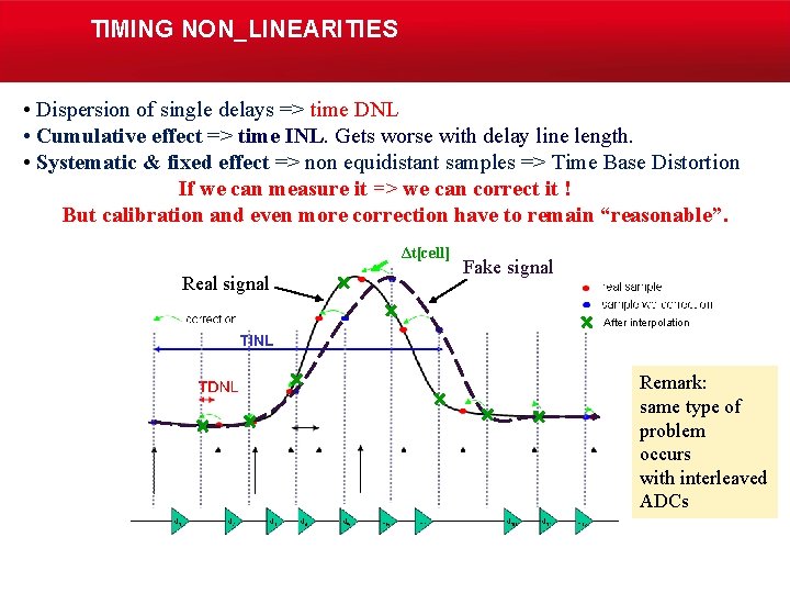
TIMING NON_LINEARITIES • Dispersion of single delays => time DNL • Cumulative effect => time INL. Gets worse with delay line length. • Systematic & fixed effect => non equidistant samples => Time Base Distortion If we can measure it => we can correct it ! But calibration and even more correction have to remain “reasonable”. Δt[cell] Real signal Fake signal After interpolation Remark: same type of problem occurs with interleaved ADCs

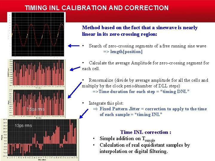
TIMING INL CALIBRATION AND CORRECTION Method based on the fact that a sinewave is nearly linear in its zero crossing region: • Search of zero-crossing segments of a free running sine wave => length[position] • Calculate the average Amplitude for zero-crossing segment for each cell. • Renormalize (divide by average amplitude for all the cells and multiply by the clock period/number of DLL steps) =>Time duration for each step = “timing DNL” • 7. 5 ps rms Integrate this plot: Þ Fixed Pattern Jitter = correction to apply to the time of each sample = “timing INL” 13 ps rms Time INL correction : • Simple addition on Tsample • Calculation of real equidistant samples by interpolation or digital filtering.

SAMPIC DIGITIZATION/NOISE § Wilkinson conversion works as expected with 1. 3 GHz clock § 0. 5 m. V /ADC count § 1 V dynamic/ 11 bit in 1. 6µs § Cell/cell pedestal spread = 5 m. V rms => easily calibrated and corrected § After correction: average noise is 1 m. V rms § Noisiest cells are at 1. 5 m. V rms § unchanged with sampling frequency § Also tested in 9 bit mode • LSB = 2 m. V • Only 15% noise increase § ~10 bit rms range | PAGE 41