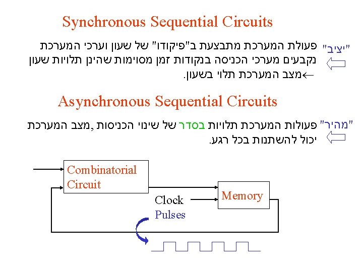
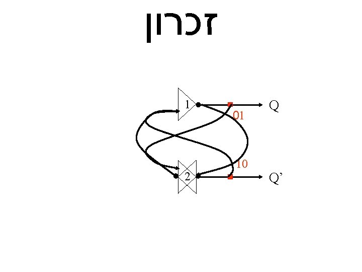
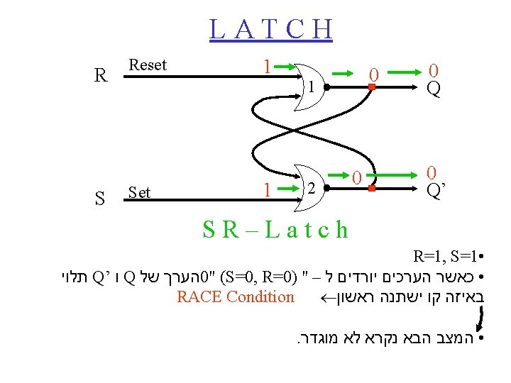
LATCH R S Reset O 0 Set 1


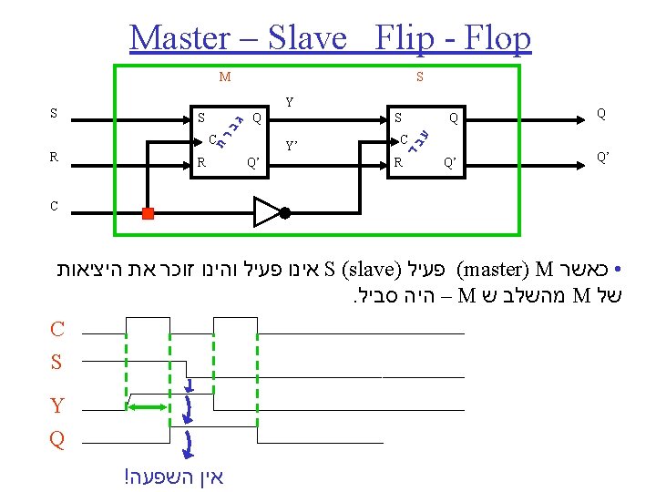


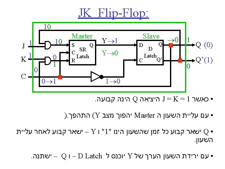
 Flip-Flop Master Y T S SR Q C Latch R Slave D")
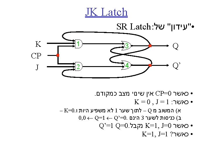
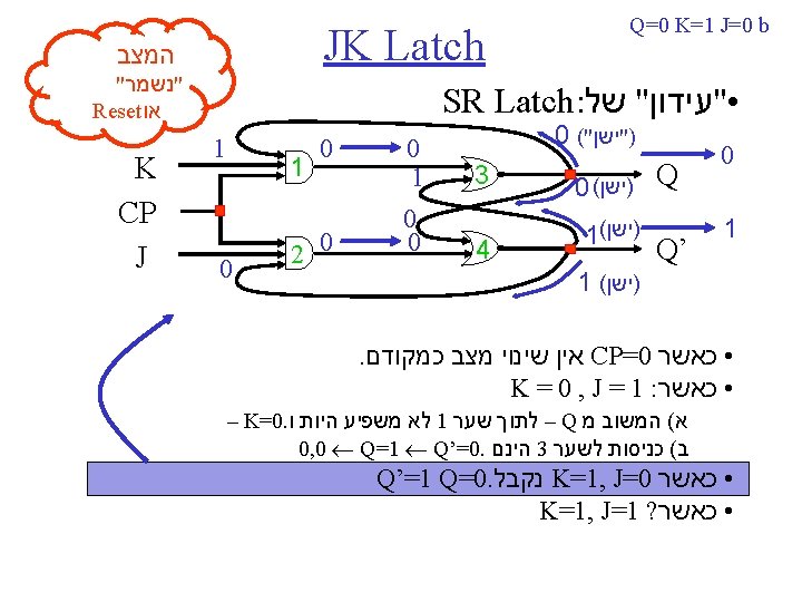
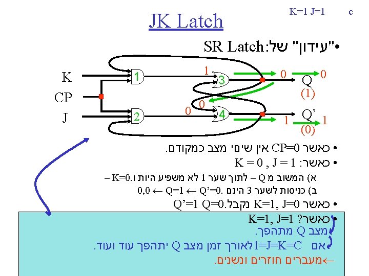
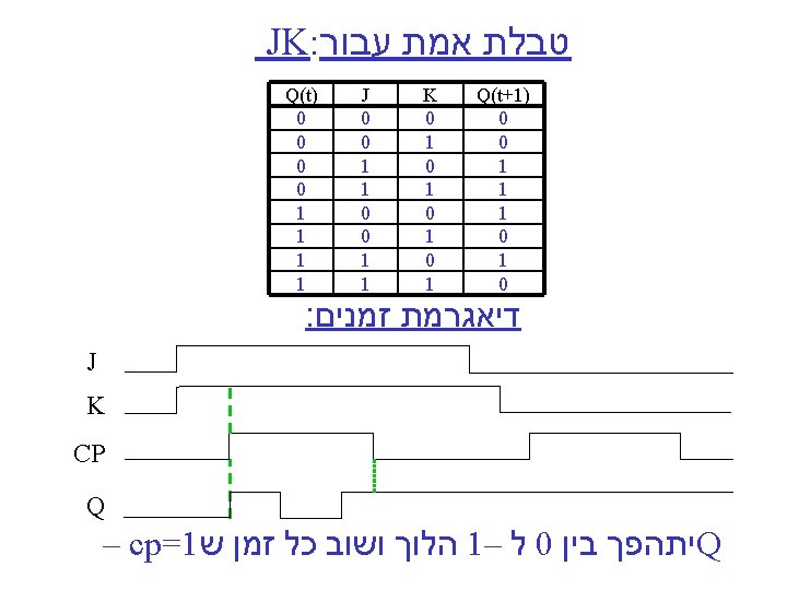
 שינוי של קלט t+1 Q(t) שינוי של פלט JKFF")


 Undefined instruction c 0 00")


- Slides: 68
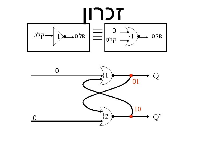
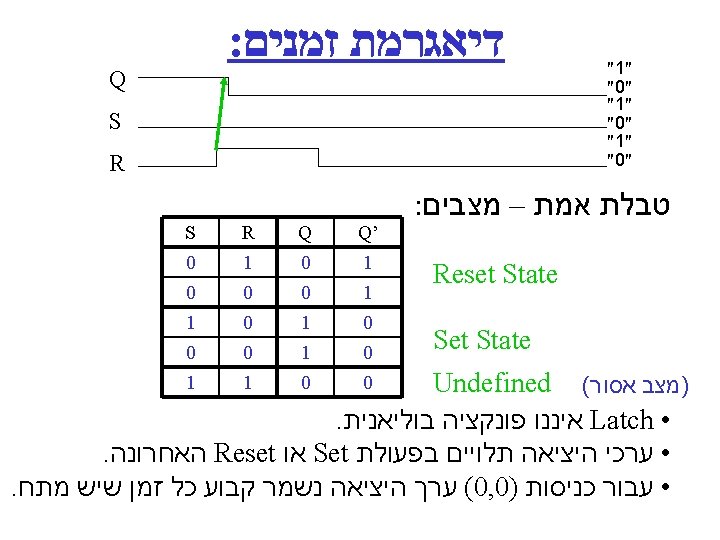
LATCH R S Reset O 0 Set 1 1 1 0 2 0 SR–Latch 1 Q 0 Q’
LATCH R Reset 1 1 0 0 Q 1 1 Q’ 0 S Set 0 0 0 2 SR–Latch
SR Latch with NAND R 1 0 0 1 S S 0 1 1 1 0 R 1 1 0 Q’ 1 1 0 0 1 Q 0 0 1 1 1 Q Q’ Set State Reset State Undefined Set Command 1 0 Reset Command 1 0
SR Latch with NAND R 1 0 0 1 S S 0 1 1 1 0 R 1 1 0 Q’ 1 1 0 0 1 Q 0 0 1 1 1 Q Q’ Set State Reset State Undefined Set Command 1 0 Reset Command 1 0
: מבוקר שעון SR Latch R R Clock Pulse CP 0 1 Q’ S S 0 S R CP Q Q C S R Next Q 0 No change 1 1 0 Q=1 1 0 1 Q=0 1 1 1 Undef 1 0 0 No change
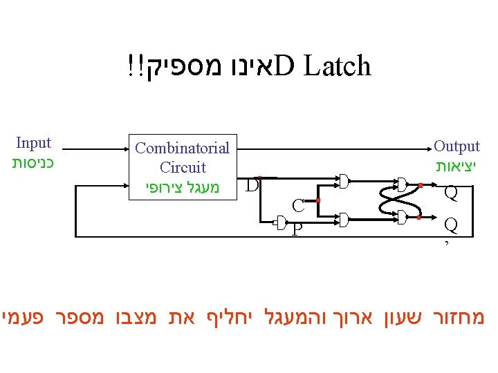
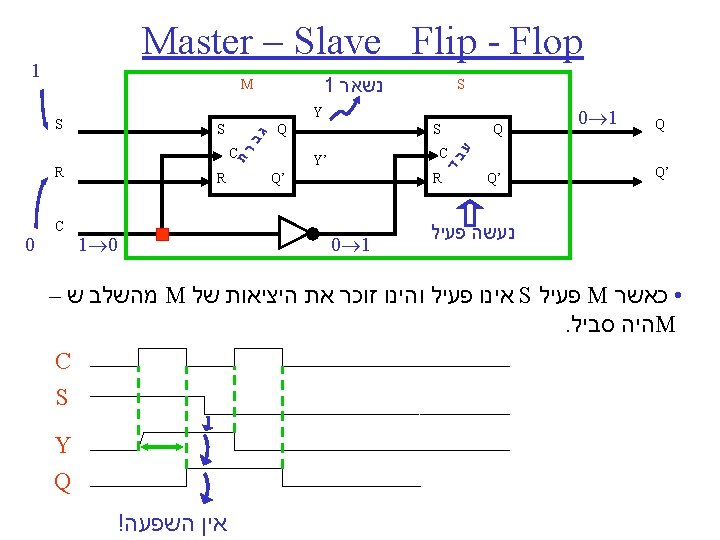
!! כן מספיק D Flip Flop C M S C R Q Q ’ Y Y’ S S C R עב ד Combinatorial Circuit S מעגל צירופי R ב ג ת ר Input כניסות Q Q ’ Q
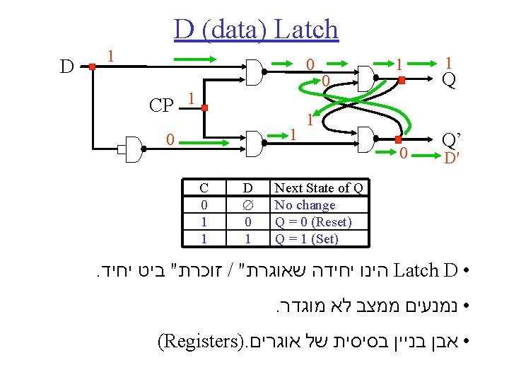
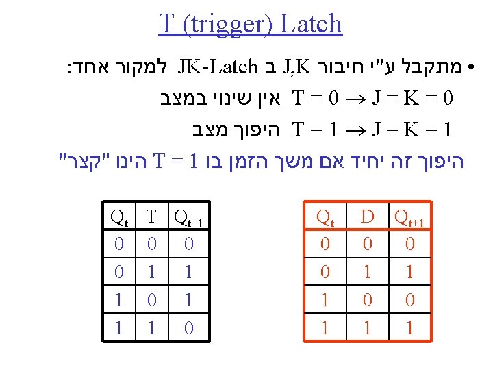
T (trigger) Flip-Flop Master Y T S SR Q C Latch R Slave D D Q Latch Q’ C Q Q’ Q(t) T=1 Q’(t+1) T=0 Q(t) D (data) Flip-Flop D Master Y D D C Latch Q(t+1) D(t) Slave D C D Latch Q
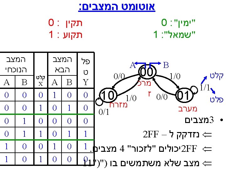
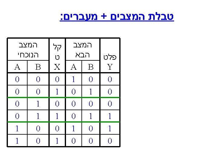
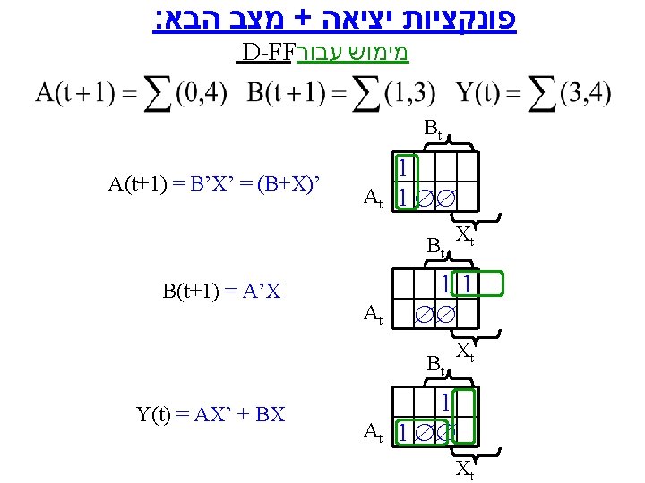
: טבלאות המצבים t Q(t) שינוי של קלט t+1 Q(t) שינוי של פלט JKFF J 0 0 1 1 K Q(t+1) 0 Q(t) No Change 1 0 Reset 0 1 Set 1 Q’(t) Complement DFF D Q(t+1) 0 0 Reset 1 1 Set SRFF S 0 0 1 1 R Q(t+1) 0 Q(t) No Change 1 0 Reset 0 1 Set 1 ? Undef. TFF T Q(t+1) 0 Q(t) No Change 1 Q’(t) Complement
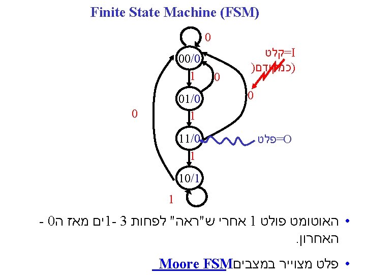
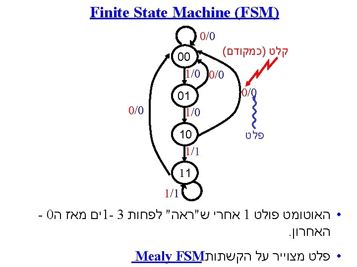
–Moore טבלת המצבים 0 00/0 1 01/0 1 11/0 1 0 10/1 1 0 0 At 0 0 1 1 Bt 0 1 1 0 I=1 At+1 Bt+1 0 0 0 1 0 – A & B הפלט תלוי ב Ot 0 0 0 1
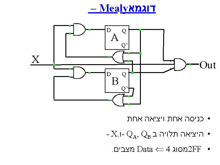
- Mealy טבלת המצבים At 0 0 1 1 Bt 0 1 X=0 X=1 At+1 Bt+1 Ot Ot 0 0 0 1 0 0 0 0 0 1 1 0 1 - X הפלט תלוי ב
– Moore טבלת המצבים 0 00/0 1 0 At 0 0 1 1 01/0 1 11/0 1 0 0 10/1 1 Bt+1 0 1 I=0 I=1 At+1 Bt+1 0 0 0 1 0 Bt 0 1 1 0 AB 00 01 Ot 0 0 0 1 AB 11 10 I At+1 0 1 00 01 11 10
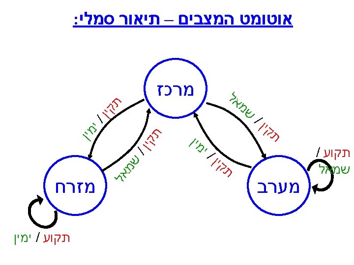
Graphical Specification of FSM
Finite State Machine for Control 0 0 1 1 0 1 0 1 0 1 1 1 0 0 0 1 1 1 0 0 0 0 1
The control signals decoder We just implement the table of slide 54: Let’s look at ALUSrc. A: it is “ 0” in states 0 and 1 and it is “ 1” in states 2, 6 and 8. In all other states we don’t care. let’s look at PCWrite: it is “ 1” in states 0 and 9. In all other states it must be “ 0”. And so, we’ll fill the table below and build the decoder. state Control signals S 3 S 2 S 1 S 0 fetch 0 0 0 1 0 decode 0 0 0 1 0 0 0 Adr. Cmp 0 0 1 0 0 load 0 0 1 1 X 0 0 WB 0 1 0 0 X 0 0 store 0 1 X 0 0 ALU 0 1 1 0 0 WBR 0 1 1 1 X 0 0 branch 1 0 0 0 1 jump 1 0 0 1 X 1 0 X 0 0 All other combinations ALUSrc. A PCWrite. Cond
The state machine “next state calc. ” logic opcode current state IR 31 IR 30 IR 29 IR 28 IR 27 IR 26 S 3 X R-type lw+sw 0 1 X 0 X next state S 2 S 1 S 0 S 3 S 2 S 1 S 0 X X 0 0 0 0 1 0 1 1 0 X X 0 0 0 1 0 Fetch 0 Decode Adr. Cmp lw sw X X 0 1 X X X 0 0 1 0 0 0 1 1 X 0 0 1 0 1 1 lw+sw R-type 2 sw lw Load ALU 6 Store 3 5 WB 4 R-type=000000, lw=100011, sw=101011, beq=000100, bne=000101, lui=001111, j=0000010, jal=000011, addi=001000 WBR 7 beq j Branch 8 Jump 9
Interrupt and exception Type of event From Where ? Interrupt MIPS terminology External I/O device request ------------------------------------------Invoke Operation system Internal Exception From user program ------------------------------------------Arithmetic Overflow Internal Exception ------------------------------------------Using an undefined Instruction Internal Exception -------------------------------------------Hardware malfunctions Either Exception or interrupt
Exceptions handling Exception type Exception vector address (in hex) Undefined instruction c 0 00 00 00 Arithmetic Overflow c 0 00 00 20 We have 2 ways to handle exceptions: Cause register or Vectored interrupts MIPS – Cause register
Handling exceptions
Handling exceptions
Handling interrupts: Save. PC Jump. Int 11 10 Fetch 0 IRET 1 Decode 1 lw+sw Adr. Cmp ALU 2 lw Load 3 R-type s w 6 Store 5 WB 4 WBR 7 j beq Branch 8 Jump 9
PLA Implementation • If I picked a horizontal or vertical line could you explain it?
ROM Implementation • ROM = "Read Only Memory" – values of memory locations are fixed ahead of time • A ROM can be used to implement a truth table – if the address is m-bits, we can address 2 m entries in the ROM. – our outputs are the bits of data that the address points to. 0 0 0 1 1 m n 0 0 0 1 1 0 0 1 1 1 0 1 0 1 1 0 0 0 1 1 m is the "heigth", and n is the "width" 0 0 0 1 1 0 0 1 0 1
ROM Implementation • How many inputs are there? 6 bits for opcode, 4 bits for state = 10 address lines (i. e. , 210 = 1024 different addresses) • How many outputs are there? 16 datapath-control outputs, 4 state bits = 20 outputs • ROM is 210 x 20 = 20 K bits size) (and a rather unusual • Rather wasteful, since for lots of the entries, the outputs are the same — i. e. , opcode is often ignored
ROM vs PLA • Break up the table into two parts — 4 state bits tell you the 16 outputs, 24 x 16 bits of ROM — 10 bits tell you the 4 next state bits, 210 x 4 bits of ROM — Total: 4. 3 K bits of ROM • PLA is much smaller — can share product terms — only need entries that produce an active output — can take into account don't cares • Size is (#inputs #product-terms) + (#outputs #product-terms) For this example = (10 x 17)+(20 x 17) = 460 PLA cells • PLA cells usually about the size of a ROM cell (slightly bigger)
Microprogramming
Microprogramming • A specification methodology – appropriate if hundreds of opcodes, modes, cycles, etc. – signals specified symbolically using microinstructions • Will two implementations of the same architecture have the same microcode? • What would a microassembler do?
Details
Microinstruction format
Maximally vs. Minimally Encoded • No encoding: – 1 bit for each datapath operation – faster, requires more memory (logic) – used for Vax 780 — an astonishing 400 K of memory! • Lots of encoding: – send the microinstructions through logic to get control signals – uses less memory, slower • Historical context of CISC: – Too much logic to put on a single chip with everything else – Use a ROM (or even RAM) to hold the microcode – It’s easy to add new instructions
Microcode: Trade-offs • Distinction between specification and implementation is sometimes blurred • Specification Advantages: – Easy to design and write – Design architecture and microcode in parallel • Implementation (off-chip ROM) Advantages – Easy to change since values are in memory – Can emulate other architectures – Can make use of internal registers • Implementation Disadvantages, SLOWER now that: – Control is implemented on same chip as processor – ROM is no longer faster than RAM – No need to go back and make changes
o and micro - instruction” Interpretation Main Memory ADD SUB AND . . . DATA execution unit CPU control memory User program plus Data this can change! one of these is mapped into one of these AND microsequence e. g. , Fetch Calc Operand Addr Fetch Operand(s) Calculate Save Answer(s)
The Big Picture
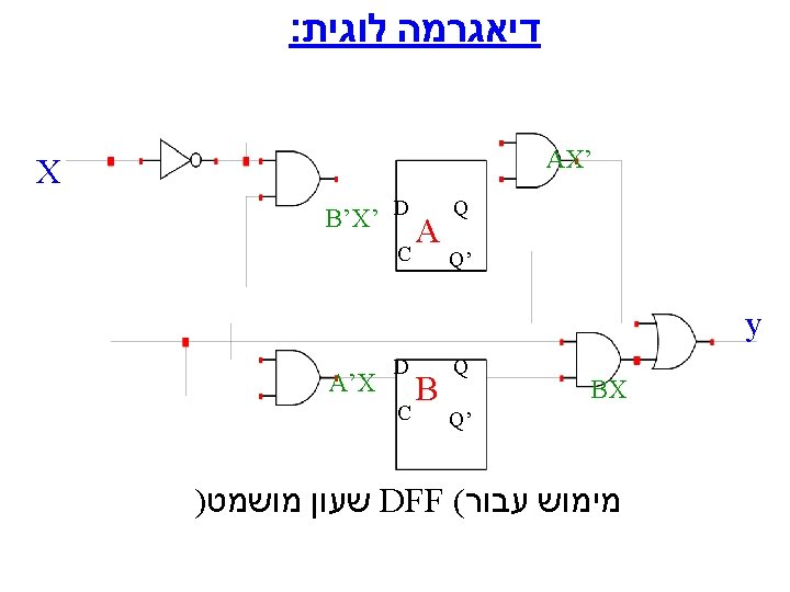
: מעגלים סדרתיים – תזמון MSJFF YA J CP K Q A Q’ MSJFF YB J CP K Q B Q’ D(t-2) CP YA QA YB QB : דוגמא Out(t) 2 JKFF