
LaserScribing and Al 2 O 3 Sidewall Passivation
Laser-Scribing and Al 2 O 3 Sidewall Passivation of P-Type Sensors Marc Christophersen 1, Bernard F. Phlips 1, Vitaliy Fadeyev 2, and Hartmut F. -W. Sadrozinski 2 (1) Code 7654, U. S. Naval Research Laboratory; (2) Santa Cruz Institute for Particle Physics, University of California Santa Cruz Contact: marc. christophersen@nrl. navy. mil +1 -202 -404 -2448 “ 6 th Trento Workshop”, March 2 -4, 2011 Laser-Scribing & Al 2 O 3 Sidewall Passivation of P-Type 1
Outline • Slim Edges – Motivation and Approaches • Laser-Scribing and Cleaving • Results for N-Type Sensors - Laser Parameters - IV Curves for N-Type Sensors • Results for P-Type Sensors - Alumina for P-Type Silicon Passivation - Introduction into Atomic Layer Deposition (ALD) - Silvaco Simulations for P-Type sensors - IV Curves for P-Type Diodes with Alumina Passivation • Conclusions and Outlook “ 6 th Trento Workshop”, March 2 -4, 2011 Laser-Scribing & Al 2 O 3 Sidewall Passivation of P-Type 2
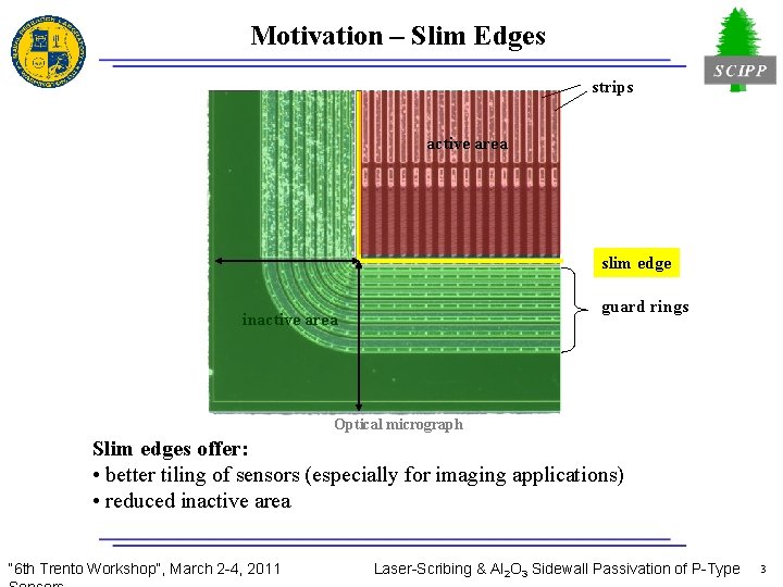
Motivation – Slim Edges strips active area slim edge guard rings inactive area Optical micrograph Slim edges offer: • better tiling of sensors (especially for imaging applications) • reduced inactive area “ 6 th Trento Workshop”, March 2 -4, 2011 Laser-Scribing & Al 2 O 3 Sidewall Passivation of P-Type 3
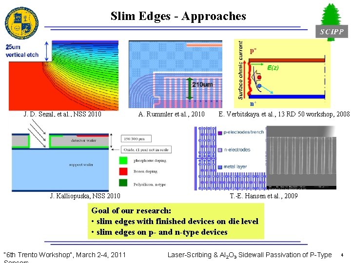
Slim Edges - Approaches J. D. Segal, et al. , NSS 2010 J. Kalliopuska, NSS 2010 A. Rummler et al. , 2010 E. Verbitskaya et al. , 13 RD 50 workshop, 2008 T. -E. Hansen et al. , 2009 Goal of our research: • slim edges with finished devices on die level • slim edges on p- and n-type devices “ 6 th Trento Workshop”, March 2 -4, 2011 Laser-Scribing & Al 2 O 3 Sidewall Passivation of P-Type 4
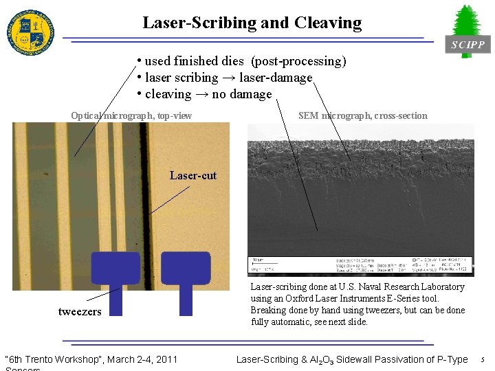
Laser-Scribing and Cleaving • used finished dies (post-processing) • laser scribing → laser-damage • cleaving → no damage Optical micrograph, top-view SEM micrograph, cross-section Laser-cut tweezers “ 6 th Trento Workshop”, March 2 -4, 2011 Laser-scribing done at U. S. Naval Research Laboratory using an Oxford Laser Instruments E-Series tool. Breaking done by hand using tweezers, but can be done fully automatic, see next slide. Laser-Scribing & Al 2 O 3 Sidewall Passivation of P-Type 5
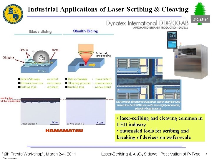
Industrial Applications of Laser-Scribing & Cleaving • laser-scribing and cleaving common in LED industry • automated tools for scribing and breaking of devices on wafer-scale “ 6 th Trento Workshop”, March 2 -4, 2011 Laser-Scribing & Al 2 O 3 Sidewall Passivation of P-Type 6
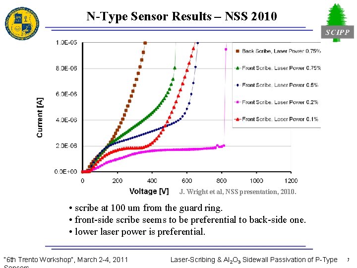
N-Type Sensor Results – NSS 2010 J. Wright et al, NSS presentation, 2010. • scribe at 100 um from the guard ring. • front-side scribe seems to be preferential to back-side one. • lower laser power is preferential. “ 6 th Trento Workshop”, March 2 -4, 2011 Laser-Scribing & Al 2 O 3 Sidewall Passivation of P-Type 7
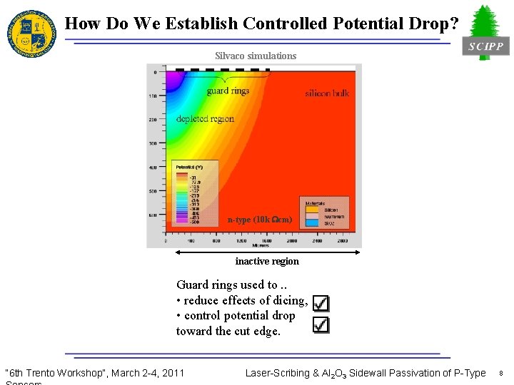
How Do We Establish Controlled Potential Drop? Silvaco simulations n-type (10 k Wcm) inactive region Guard rings used to. . • reduce effects of dicing, • control potential drop toward the cut edge. “ 6 th Trento Workshop”, March 2 -4, 2011 Laser-Scribing & Al 2 O 3 Sidewall Passivation of P-Type 8
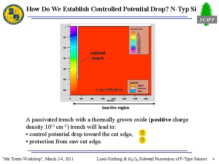
How Do We Establish Controlled Potential Drop? N-Typ Si oxidized trench n-type (10 k Wcm) inactive region A passivated trench with a thermally grown oxide (positive charge density 1011 cm-2) trench will lead to: • control potential drop toward the cut edge, • protection from saw cut edge. “ 6 th Trento Workshop”, March 2 -4, 2011 Laser-Scribing & Al 2 O 3 Sidewall Passivation of P-Type Sensors 9
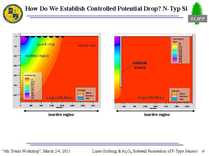
How Do We Establish Controlled Potential Drop? N-Typ Si oxidized trench n-type (10 k Wcm) inactive region “ 6 th Trento Workshop”, March 2 -4, 2011 n-type (10 k Wcm) inactive region Laser-Scribing & Al 2 O 3 Sidewall Passivation of P-Type Sensors 10
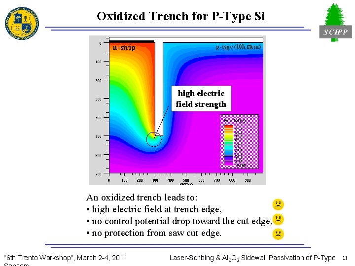
Oxidized Trench for P-Type Si n-strip p-type (10 k Wcm) high electric field strength An oxidized trench leads to: • high electric field at trench edge, • no control potential drop toward the cut edge, • no protection from saw cut edge. “ 6 th Trento Workshop”, March 2 -4, 2011 Laser-Scribing & Al 2 O 3 Sidewall Passivation of P-Type 11
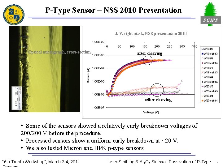
P-Type Sensor – NSS 2010 Presentation J. Wright et al. , NSS presentation 2010 Optical micrograph, cross-section after cleaving before cleaving • Some of the sensors showed a relatively early breakdown voltages of 200/300 V before the procedure. • Processed sensors show a uniform early breakdown at ~20 V. • We also tested Micron and HPK p-type sensors. “ 6 th Trento Workshop”, March 2 -4, 2011 Laser-Scribing & Al 2 O 3 Sidewall Passivation of P-Type 12
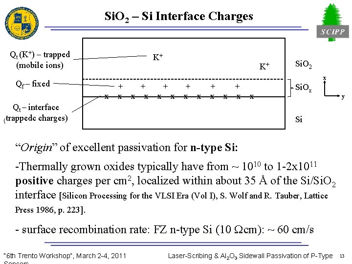
Si. O 2 – Si Interface Charges Qt (K+) – trapped (mobile ions) Qf – fixed K+ K+ Si. O 2 x + + x x x + + x x x Qt – interface (trappedc charges) x Si. Ox y Si “Origin” of excellent passivation for n-type Si: -Thermally grown oxides typically have from ~ 1010 to 1 -2 x 10¹¹ positive charges per cm 2, localized within about 35 Å of the Si/Si. O 2 interface [Silicon Processing for the VLSI Era (Vol I), S. Wolf and R. Tauber, Lattice Press 1986, p. 223]. - surface recombination rate: FZ n-type Si (10 Wcm): ~ 60 cm/s “ 6 th Trento Workshop”, March 2 -4, 2011 Laser-Scribing & Al 2 O 3 Sidewall Passivation of P-Type 13
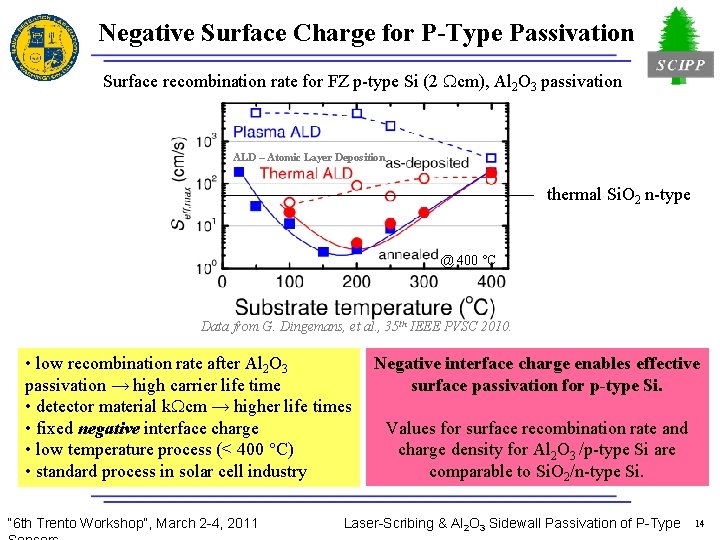
Negative Surface Charge for P-Type Passivation Surface recombination rate for FZ p-type Si (2 Wcm), Al 2 O 3 passivation ALD – Atomic Layer Deposition thermal Si. O 2 n-type @ 400 °C Data from G. Dingemans, et al. , 35 th IEEE PVSC 2010. • low recombination rate after Al 2 O 3 passivation → high carrier life time • detector material k. Wcm → higher life times • fixed negative interface charge • low temperature process (< 400 °C) • standard process in solar cell industry “ 6 th Trento Workshop”, March 2 -4, 2011 Negative interface charge enables effective surface passivation for p-type Si. Values for surface recombination rate and charge density for Al 2 O 3 /p-type Si are comparable to Si. O 2/n-type Si. Laser-Scribing & Al 2 O 3 Sidewall Passivation of P-Type 14
Introduction - ALD • Similar in chemistry to CVD (chemical vapor deposition), except that the ALD (atomic layer deposition) reaction breaks the CVD reaction into two half-reactions, keeping the precursor materials separate during the reaction. • ALD film growth is self-limited and based on surface reactions, which makes achieving atomic scale deposition control possible. • Perfect 3 -D conformality, 100% step coverage: uniform coatings on flat, inside porous and around particle samples. • Origin of negative interface charge: Functional surface groups on the silicon wafer are not optimal for an adsorption of the TMA (trimethylaluminium) precursor molecules, which leads to an incomplete reaction of the TMA and, consequently, an increased relative oxygen concentration at the interface (F. Werner et al. , 25 th European Photovoltaic Solar Energy Conference, Valencia, Spain, 6 -10 September 2010). “ 6 th Trento Workshop”, March 2 -4, 2011 Laser-Scribing & Al 2 O 3 Sidewall Passivation of P-Type 15
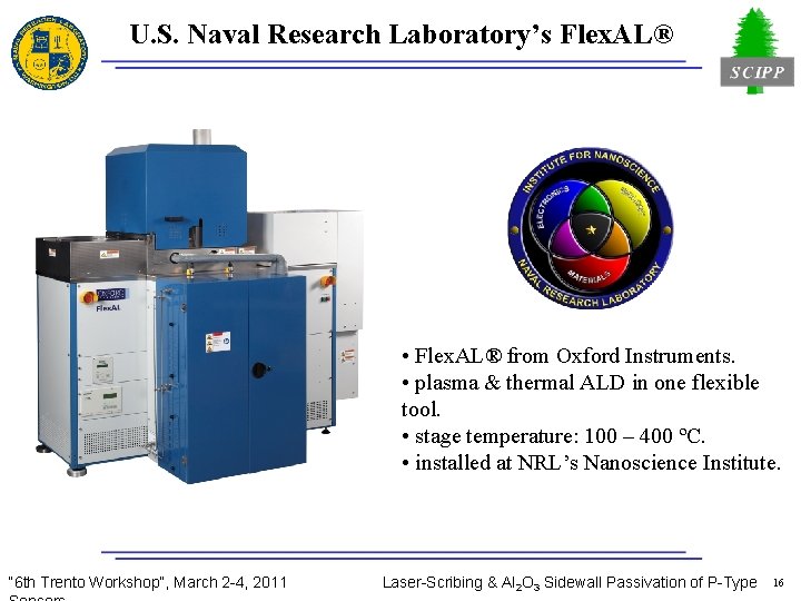
U. S. Naval Research Laboratory’s Flex. AL® • Flex. AL® from Oxford Instruments. • plasma & thermal ALD in one flexible tool. • stage temperature: 100 – 400 ºC. • installed at NRL’s Nanoscience Institute. “ 6 th Trento Workshop”, March 2 -4, 2011 Laser-Scribing & Al 2 O 3 Sidewall Passivation of P-Type 16
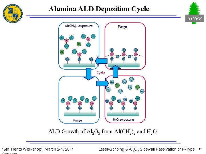
Alumina ALD Deposition Cycle ALD Growth of Al 2 O 3 from Al(CH 3)3 and H 2 O “ 6 th Trento Workshop”, March 2 -4, 2011 Laser-Scribing & Al 2 O 3 Sidewall Passivation of P-Type 17
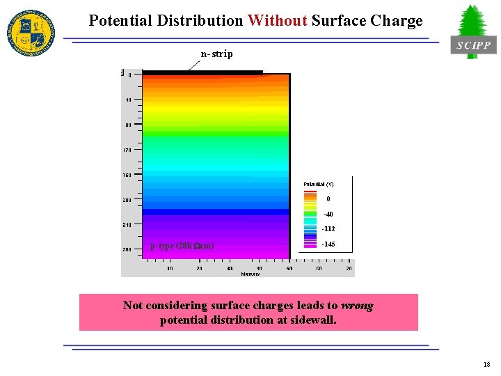
Potential Distribution Without Surface Charge n-strip 0 -40 -112 p-type (20 k Wcm) -145 Not considering surface charges leads to wrong potential distribution at sidewall. 18
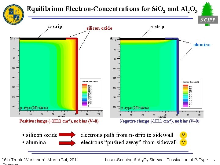
Equilibrium Electron-Concentrations for Si. O 2 and Al 2 O 3 n-strip silicon oxide alumina p-type (20 k Wcm) Positive charge (+1 E 11 cm-2), no bias (V=0) • silicon oxide • alumina “ 6 th Trento Workshop”, March 2 -4, 2011 Negative charge (-1 E 11 cm-2), no bias (V=0) electrons path from n-strip to sidewall electrons “pushed away” from sidewall Laser-Scribing & Al 2 O 3 Sidewall Passivation of P-Type 19
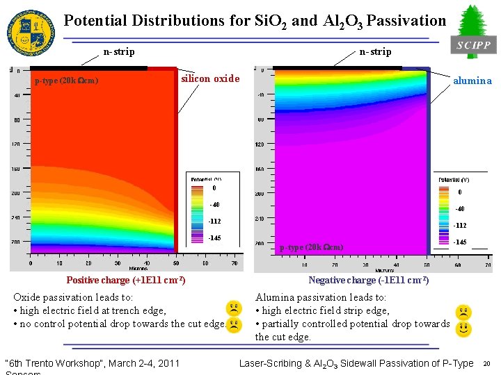
Potential Distributions for Si. O 2 and Al 2 O 3 Passivation n-strip p-type (20 k Wcm) n-strip silicon oxide alumina 0 0 -40 -112 -145 Positive charge (+1 E 11 cm-2) Oxide passivation leads to: • high electric field at trench edge, • no control potential drop towards the cut edge. “ 6 th Trento Workshop”, March 2 -4, 2011 -112 p-type (20 k Wcm) -145 Negative charge (-1 E 11 cm-2) Alumina passivation leads to: • high electric field strip edge, • partially controlled potential drop towards the cut edge. Laser-Scribing & Al 2 O 3 Sidewall Passivation of P-Type 20
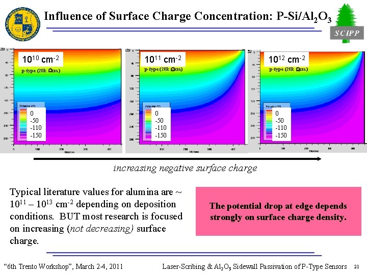
Influence of Surface Charge Concentration: P-Si/Al 2 O 3 1010 cm-2 1011 cm-2 p-type (20 k Wcm) 0 -50 -110 -150 1012 cm-2 p-type (20 k Wcm) 0 -50 -110 -150 increasing negative surface charge Typical literature values for alumina are ~ 1011 – 1013 cm-2 depending on deposition conditions. BUT most research is focused on increasing (not decreasing) surface charge. “ 6 th Trento Workshop”, March 2 -4, 2011 The potential drop at edge depends strongly on surface charge density. Laser-Scribing & Al 2 O 3 Sidewall Passivation of P-Type Sensors 21
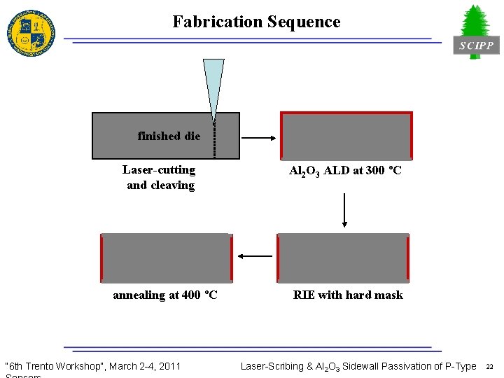
Fabrication Sequence finished die Laser-cutting and cleaving annealing at 400 ºC “ 6 th Trento Workshop”, March 2 -4, 2011 Al 2 O 3 ALD at 300 ºC RIE with hard mask Laser-Scribing & Al 2 O 3 Sidewall Passivation of P-Type 22
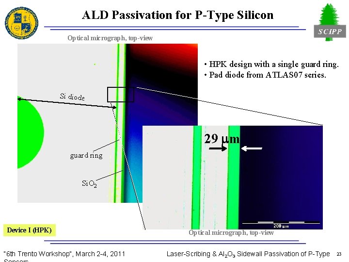
ALD Passivation for P-Type Silicon Optical micrograph, top-view • HPK design with a single guard ring. • Pad diode from ATLAS 07 series. Si diode 29 mm guard ring Si. O 2 Device I (HPK) “ 6 th Trento Workshop”, March 2 -4, 2011 Optical micrograph, top-view Laser-Scribing & Al 2 O 3 Sidewall Passivation of P-Type 23
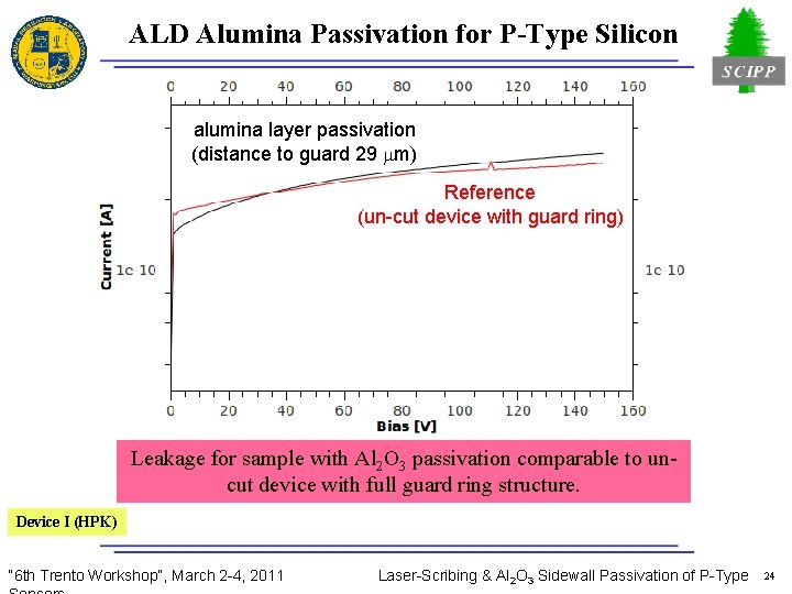
ALD Alumina Passivation for P-Type Silicon alumina layer passivation (distance to guard 29 mm) Reference (un-cut device with guard ring) Leakage for sample with Al 2 O 3 passivation comparable to uncut device with full guard ring structure. Device I (HPK) “ 6 th Trento Workshop”, March 2 -4, 2011 Laser-Scribing & Al 2 O 3 Sidewall Passivation of P-Type 24
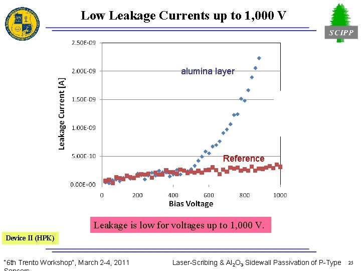
Low Leakage Currents up to 1, 000 V alumina layer Reference Leakage is low for voltages up to 1, 000 V. Device II (HPK) “ 6 th Trento Workshop”, March 2 -4, 2011 Laser-Scribing & Al 2 O 3 Sidewall Passivation of P-Type 25
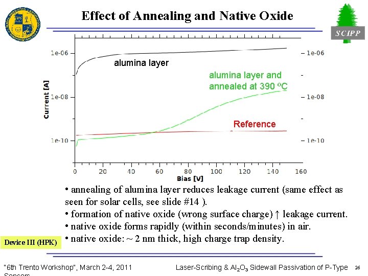
Effect of Annealing and Native Oxide alumina layer and annealed at 390 ºC Reference Device III (HPK) • annealing of alumina layer reduces leakage current (same effect as seen for solar cells, see slide #14 ). • formation of native oxide (wrong surface charge) ↑ leakage current. • native oxide forms rapidly (within seconds/minutes) in air. • native oxide: ~ 2 nm thick, high charge trap density. “ 6 th Trento Workshop”, March 2 -4, 2011 Laser-Scribing & Al 2 O 3 Sidewall Passivation of P-Type 26
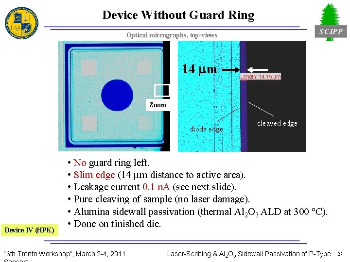
Device Without Guard Ring Optical micrographs, top-views 14 mm Zoom diode edge Device IV (HPK) cleaved edge • No guard ring left. • Slim edge (14 mm distance to active area). • Leakage current 0. 1 n. A (see next slide). • Pure cleaving of sample (no laser damage). • Alumina sidewall passivation (thermal Al 2 O 3 ALD at 300 °C). • Done on finished die. “ 6 th Trento Workshop”, March 2 -4, 2011 Laser-Scribing & Al 2 O 3 Sidewall Passivation of P-Type 27
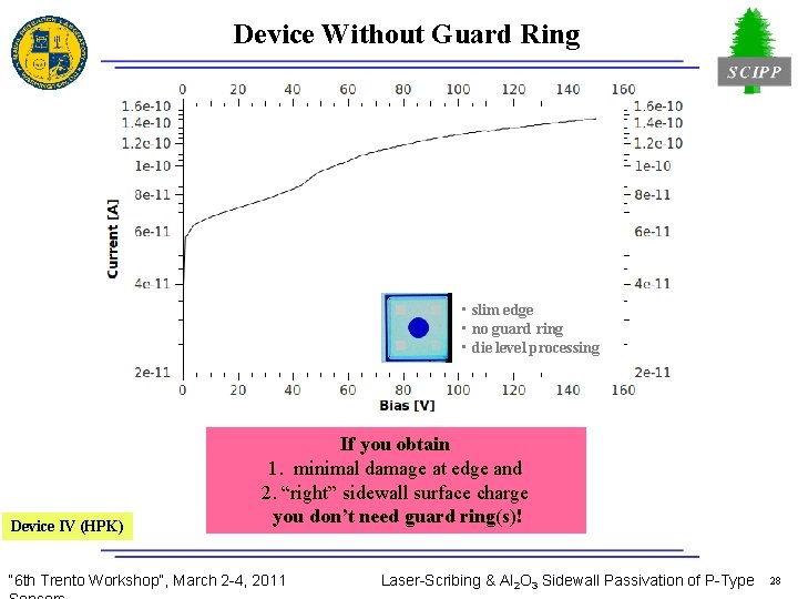
Device Without Guard Ring • slim edge • no guard ring • die level processing Device IV (HPK) If you obtain 1. minimal damage at edge and 2. “right” sidewall surface charge you don’t need guard ring(s)! “ 6 th Trento Workshop”, March 2 -4, 2011 Laser-Scribing & Al 2 O 3 Sidewall Passivation of P-Type 28
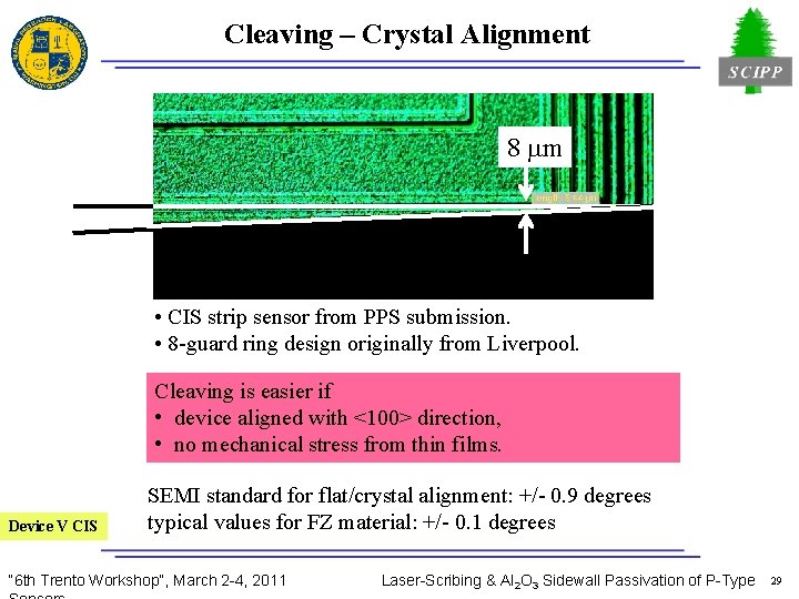
Cleaving – Crystal Alignment 8 mm • CIS strip sensor from PPS submission. • 8 -guard ring design originally from Liverpool. Cleaving is easier if • device aligned with <100> direction, • no mechanical stress from thin films. Device V CIS SEMI standard for flat/crystal alignment: +/- 0. 9 degrees typical values for FZ material: +/- 0. 1 degrees “ 6 th Trento Workshop”, March 2 -4, 2011 Laser-Scribing & Al 2 O 3 Sidewall Passivation of P-Type 29
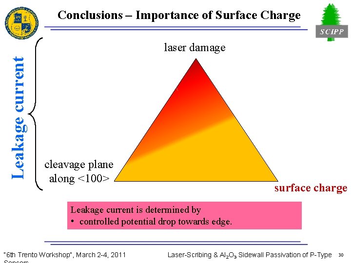
Conclusions – Importance of Surface Charge Leakage current laser damage cleavage plane along <100> surface charge Leakage current is determined by • controlled potential drop towards edge. “ 6 th Trento Workshop”, March 2 -4, 2011 Laser-Scribing & Al 2 O 3 Sidewall Passivation of P-Type 30
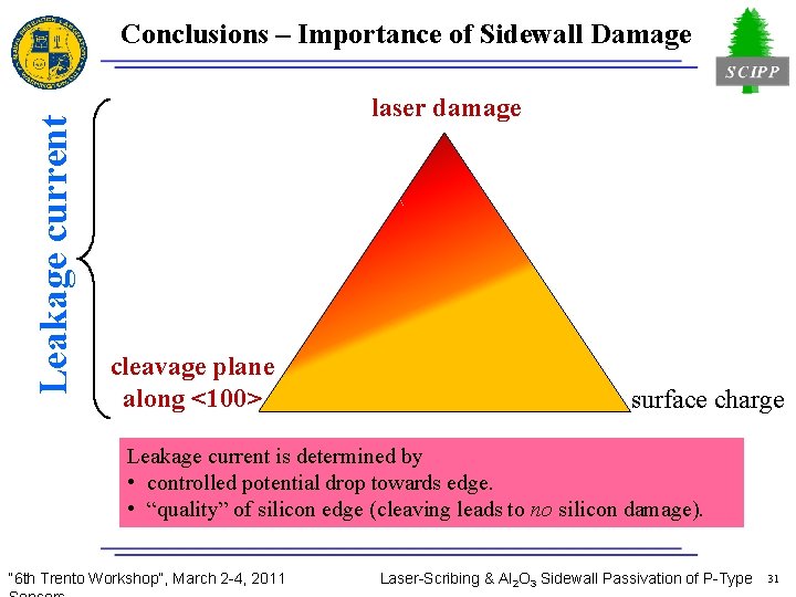
Leakage current Conclusions – Importance of Sidewall Damage laser damage cleavage plane along <100> surface charge Leakage current is determined by • controlled potential drop towards edge. • “quality” of silicon edge (cleaving leads to no silicon damage). “ 6 th Trento Workshop”, March 2 -4, 2011 Laser-Scribing & Al 2 O 3 Sidewall Passivation of P-Type 31
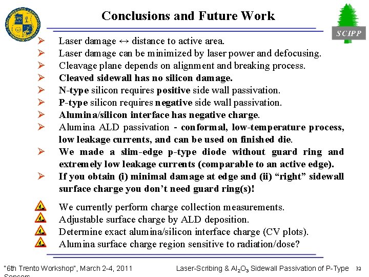
Conclusions and Future Work Ø Ø Ø Ø Laser damage ↔ distance to active area. Laser damage can be minimized by laser power and defocusing. Cleavage plane depends on alignment and breaking process. Cleaved sidewall has no silicon damage. N-type silicon requires positive side wall passivation. P-type silicon requires negative side wall passivation. Alumina/silicon interface has negative charge. Alumina ALD passivation - conformal, low-temperature process, low leakage currents, and can be used on finished die. We made a slim-edge p-type diode without guard ring and extremely low leakage currents (comparable to an active edge). If you obtain (i) minimal damage at edge and (ii) “right” sidewall surface charge you don’t need guard ring(s)! We currently perform charge collection measurements. Adjustable surface charge by ALD deposition. Determine exact alumina/silicon interface charge (CV plots). Alumina surface charge region sensitive to radiation/dose? “ 6 th Trento Workshop”, March 2 -4, 2011 Laser-Scribing & Al 2 O 3 Sidewall Passivation of P-Type 32
Back-Up Slides 33
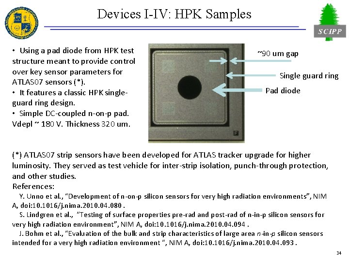
Devices I-IV: HPK Samples • Using a pad diode from HPK test structure meant to provide control over key sensor parameters for ATLAS 07 sensors (*). • It features a classic HPK singleguard ring design. • Simple DC-coupled n-on-p pad. Vdepl ~ 180 V. Thickness 320 um. ~90 um gap Single guard ring Pad diode (*) ATLAS 07 strip sensors have been developed for ATLAS tracker upgrade for higher luminosity. They served as test vehicle for inter-strip isolation, punch-through protection, and other studies. References: Y. Unno et al. , “Development of n-on-p silicon sensors for very high radiation environments”, NIM A, doi: 10. 1016/j. nima. 2010. 04. 080. S. Lindgren et al. , “Testing of surface properties pre-rad and post-rad of n-in-p silicon sensors for very high radiation environment”, NIM A, doi: 10. 1016/j. nima. 2010. 04. 094. J. Bohm et al. , “Evaluation of the bulk and strip characteristics of large area n-in-p silicon sensors intended for a very high radiation environment “, NIM A, doi: 10. 1016/j. nima. 2010. 04. 093. 34
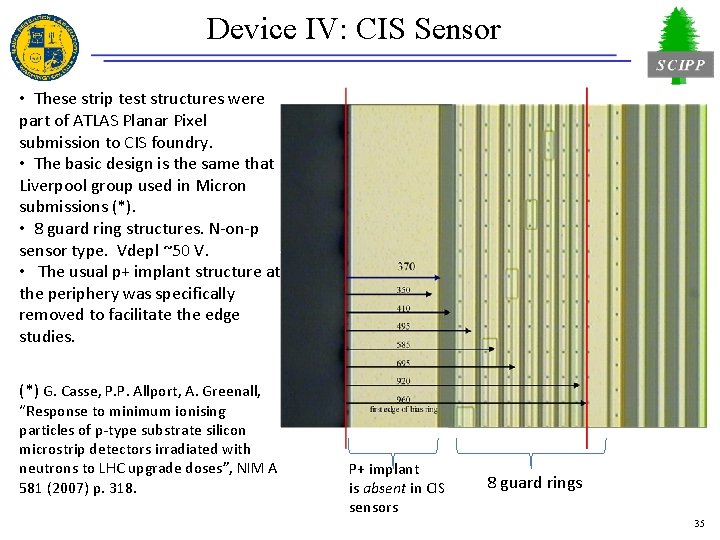
Device IV: CIS Sensor • These strip test structures were part of ATLAS Planar Pixel submission to CIS foundry. • The basic design is the same that Liverpool group used in Micron submissions (*). • 8 guard ring structures. N-on-p sensor type. Vdepl ~50 V. • The usual p+ implant structure at the periphery was specifically removed to facilitate the edge studies. (*) G. Casse, P. P. Allport, A. Greenall, “Response to minimum ionising particles of p-type substrate silicon microstrip detectors irradiated with neutrons to LHC upgrade doses”, NIM A 581 (2007) p. 318. P+ implant is absent in CIS sensors 8 guard rings 35
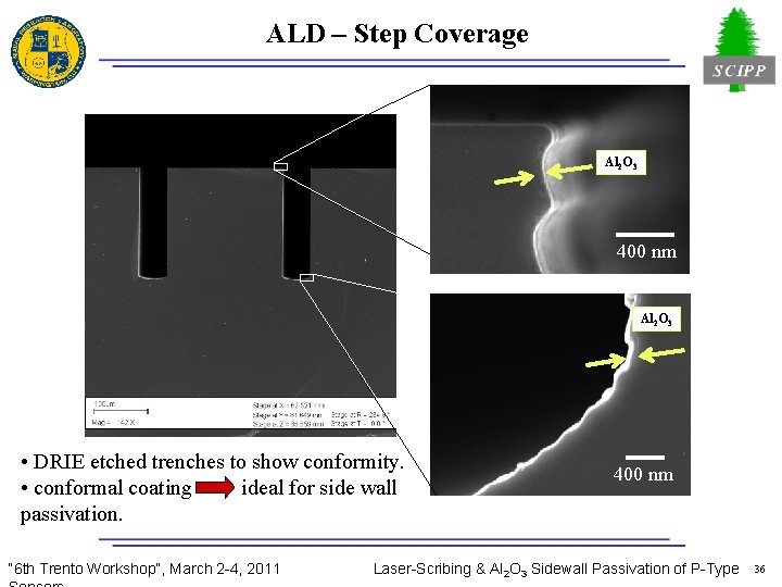
ALD – Step Coverage Al 2 O 3 400 nm Al 2 O 3 • DRIE etched trenches to show conformity. • conformal coating ideal for side wall passivation. “ 6 th Trento Workshop”, March 2 -4, 2011 400 nm Laser-Scribing & Al 2 O 3 Sidewall Passivation of P-Type 36
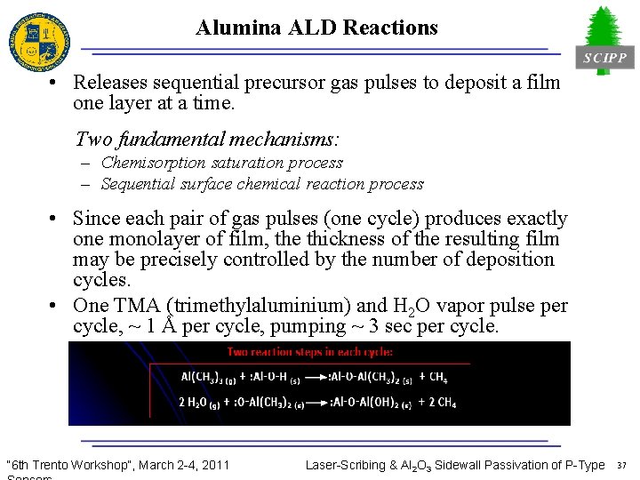
Alumina ALD Reactions • Releases sequential precursor gas pulses to deposit a film one layer at a time. Two fundamental mechanisms: – Chemisorption saturation process – Sequential surface chemical reaction process • Since each pair of gas pulses (one cycle) produces exactly one monolayer of film, the thickness of the resulting film may be precisely controlled by the number of deposition cycles. • One TMA (trimethylaluminium) and H 2 O vapor pulse per cycle, ~ 1 Å per cycle, pumping ~ 3 sec per cycle. “ 6 th Trento Workshop”, March 2 -4, 2011 Laser-Scribing & Al 2 O 3 Sidewall Passivation of P-Type 37
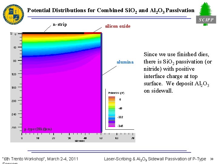
Potential Distributions for Combined Si. O 2 and Al 2 O 3 Passivation n-strip silicon oxide alumina Since we use finished dies, there is Si. O 2 passivation (or nitride) with positive interface charge at top surface. We deposit Al 2 O 3 on sidewall. 0 -40 -112 p-type (20 k Wcm) “ 6 th Trento Workshop”, March 2 -4, 2011 -145 Laser-Scribing & Al 2 O 3 Sidewall Passivation of P-Type 38
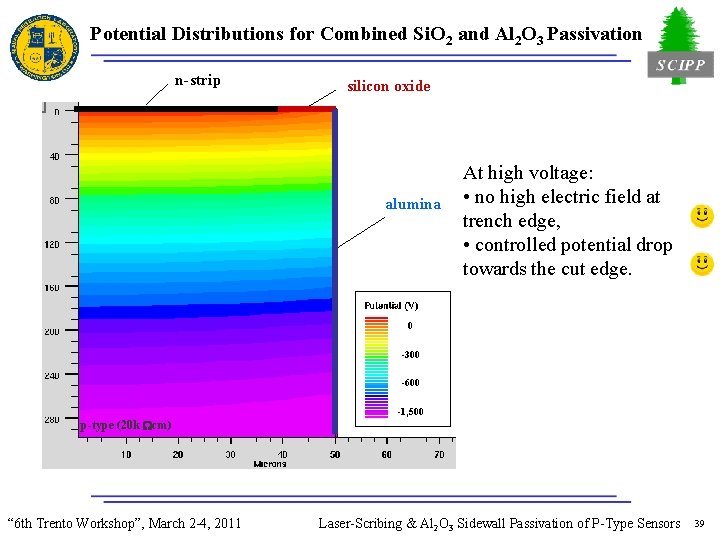
Potential Distributions for Combined Si. O 2 and Al 2 O 3 Passivation n-strip silicon oxide alumina At high voltage: • no high electric field at trench edge, • controlled potential drop towards the cut edge. 0 -300 -600 p-type (20 k Wcm) “ 6 th Trento Workshop”, March 2 -4, 2011 -1, 500 Laser-Scribing & Al 2 O 3 Sidewall Passivation of P-Type Sensors 39
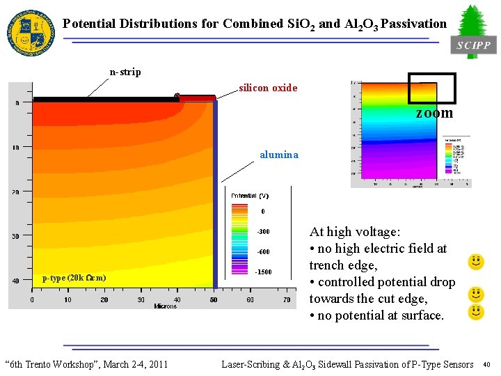
Potential Distributions for Combined Si. O 2 and Al 2 O 3 Passivation n-strip silicon oxide zoom alumina 0 -300 -600 p-type (20 k Wcm) “ 6 th Trento Workshop”, March 2 -4, 2011 -1500 At high voltage: • no high electric field at trench edge, • controlled potential drop towards the cut edge, • no potential at surface. Laser-Scribing & Al 2 O 3 Sidewall Passivation of P-Type Sensors 40
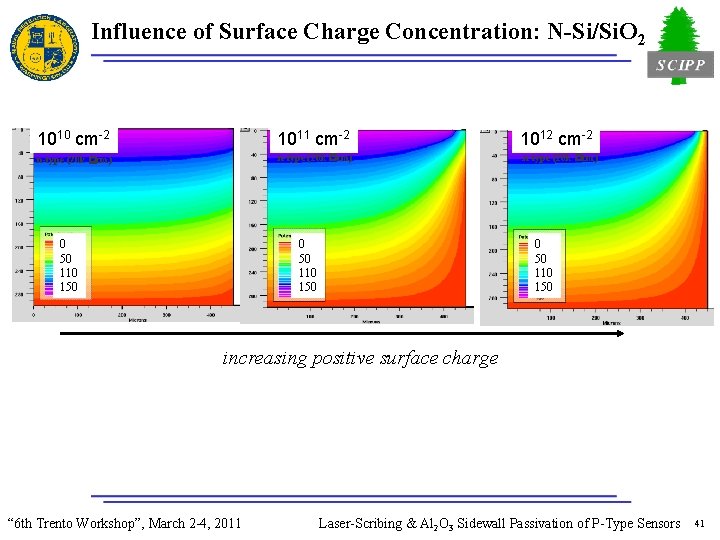
Influence of Surface Charge Concentration: N-Si/Si. O 2 1010 cm-2 1011 cm-2 n-type (20 k Wcm) 0 50 110 150 1012 cm-2 n-type (20 k Wcm) 0 50 110 150 increasing positive surface charge “ 6 th Trento Workshop”, March 2 -4, 2011 Laser-Scribing & Al 2 O 3 Sidewall Passivation of P-Type Sensors 41
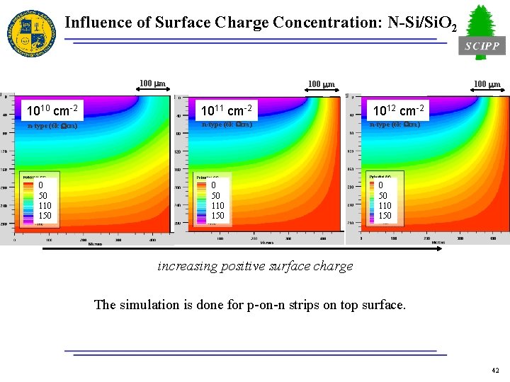
Influence of Surface Charge Concentration: N-Si/Si. O 2 100 mm 1010 cm-2 1011 cm-2 n-type (6 k Wcm) 0 50 110 150 100 mm 1012 cm-2 n-type (6 k Wcm) 0 50 110 150 increasing positive surface charge The simulation is done for p-on-n strips on top surface. 42
- Slides: 42