Large Signal Amplifier Design Ryan Child 1 Background
Large Signal Amplifier Design Ryan Child 1
Background Large Signal Amplifiers belong to a class of amplifiers that are used for applications where high current switching is needed, such as when driving: • • Electromechanical transducers (i. e. loudspeakers) Motors of rotating machines (i. e. centrifuges) When to use Small Signal and when to use Large Signal Amplifiers? • • • Small Signal Amplifiers provide voltage gain but little current gain and are incapable of switching large amounts of current. Small Signal Amplifiers may be used in the earlier stages of amplification if the input resistance of the next stage is very large. Large Signal Amplifiers are typically used in the later stages of amplification and directly drive a load, which may require large amounts of current. 2
Requirements Typical applications of the large signal amplifier lead to three primary objectives for any design: 1. Maximize output signal power (allows for driving larger loads) 2. Minimize distortion (output waveform should deviate from input waveform as little as possible) 3. Minimize quiescent power dissipation (keeps operation costs low and lengthens the life of the circuit) 3
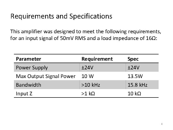
Requirements and Specifications This amplifier was designed to meet the following requirements, for an input signal of 50 m. V RMS and a load impedance of 16Ω: Parameter Power Supply Max Output Signal Power Bandwidth Requirement ± 24 V 10 W >10 k. Hz Spec ± 24 V 13. 5 W 15. 8 k. Hz Input Z >1 kΩ 10 kΩ 4
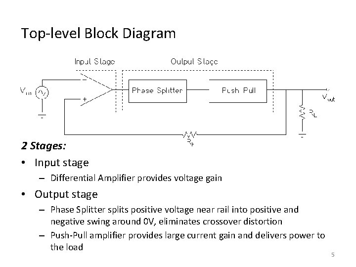
Top-level Block Diagram 2 Stages: • Input stage – Differential Amplifier provides voltage gain • Output stage – Phase Splitter splits positive voltage near rail into positive and negative swing around 0 V, eliminates crossover distortion – Push-Pull amplifier provides large current gain and delivers power to the load 5
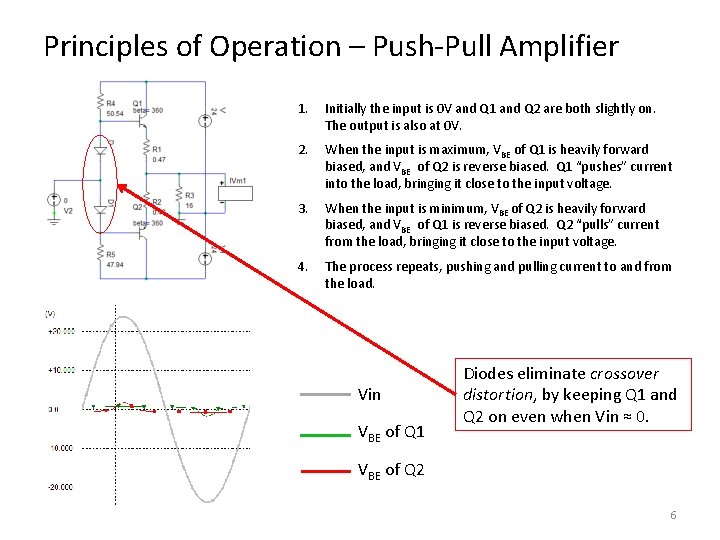
Principles of Operation – Push-Pull Amplifier 1. Initially the input is 0 V and Q 1 and Q 2 are both slightly on. The output is also at 0 V. 2. When the input is maximum, VBE of Q 1 is heavily forward biased, and VBE of Q 2 is reverse biased. Q 1 “pushes” current into the load, bringing it close to the input voltage. 3. When the input is minimum, VBE of Q 2 is heavily forward biased, and VBE of Q 1 is reverse biased. Q 2 “pulls” current from the load, bringing it close to the input voltage. 4. The process repeats, pushing and pulling current to and from the load. Vin VBE of Q 1 Diodes eliminate crossover distortion, by keeping Q 1 and Q 2 on even when Vin ≈ 0. VBE of Q 2 6

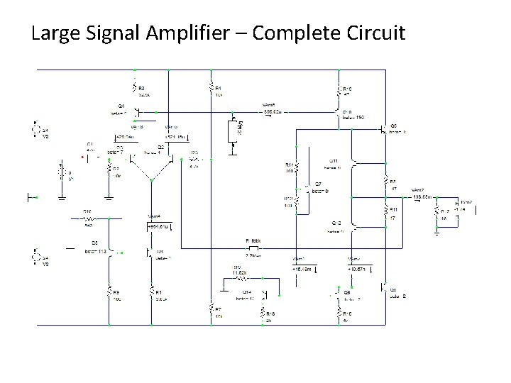
Principles of Operation – Signal Splitter ∆ϕ=180˚ 1. Initially, input is near the positive supply rail (≈ 21 V) 2. As the input falls, VBE of Q 10 increases, turning Q 10 on. Excess current goes into the base of Q 5, turning it on as well. VCE of Q 10 decreases, raising the input of the pushpull circuit. 3. When the input is minimum, Q 10 and Q 5 are fully on, and the input to the push-pull circuit is at a maximum. 4. As input rises above the initial value, VBE of Q 10 is lowered, and its emitter current is reduced. The collector current of Q 9 must remain constant, so it pulls more current from Q 6. VCE of Q 10 increases, lowering the input of the push-pull circuit. 5. When input is maximum, Q 10 and Q 5 are nearly cut off, and the input to the push-pull circuit is at a minimum. 6. Repeat Vin VBE of Q 10 VCE of Q 10 R 13, R 14 and Q 7 mimic the diodes to eliminate crossover distortion, but allow a “tunable diode drop” if a potentiometer is used. 7
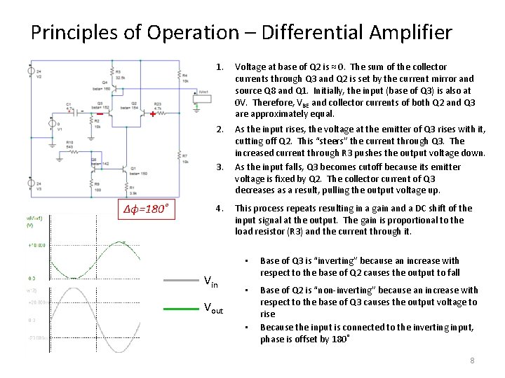
Principles of Operation – Differential Amplifier – 1. Voltage at base of Q 2 is ≈ 0. The sum of the collector currents through Q 3 and Q 2 is set by the current mirror and source Q 8 and Q 1. Initially, the input (base of Q 3) is also at 0 V. Therefore, VBE and collector currents of both Q 2 and Q 3 are approximately equal. 2. As the input rises, the voltage at the emitter of Q 3 rises with it, cutting off Q 2. This “steers” the current through Q 3. The increased current through R 3 pushes the output voltage down. As the input falls, Q 3 becomes cutoff because its emitter voltage is fixed by Q 2. The collector current of Q 3 decreases as a result, pulling the output voltage up. + 3. ∆ϕ=180˚ 4. Vin This process repeats resulting in a gain and a DC shift of the input signal at the output. The gain is proportional to the load resistor (R 3) and the current through it. • Base of Q 3 is “inverting” because an increase with respect to the base of Q 2 causes the output to fall • Base of Q 2 is “non-inverting” because an increase with respect to the base of Q 3 causes the output voltage to rise Because the input is connected to the inverting input, phase is offset by 180˚ Vout • 8
Large Signal Amplifier – Complete Circuit
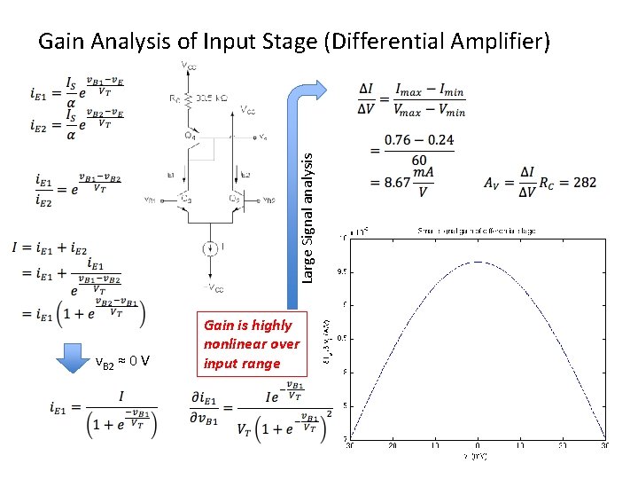
Large Signal analysis Gain Analysis of Input Stage (Differential Amplifier) v. B 2 ≈ 0 V Gain is highly nonlinear over input range
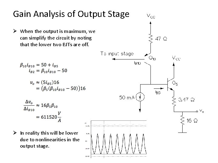
Gain Analysis of Output Stage Ø When the output is maximum, we can simplify the circuit by noting that the lower two BJTs are off. Ø In reality this will be lower due to nonlinearities in the output stage.
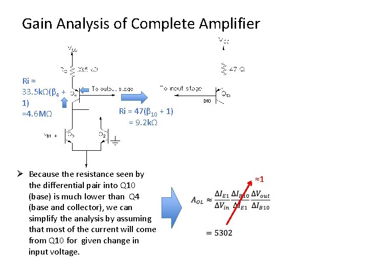
Gain Analysis of Complete Amplifier Ri ≈ 33. 5 kΩ(β 4 + 1) =4. 6 MΩ Ri = 47(β 10 + 1) = 9. 2 kΩ Ø Because the resistance seen by the differential pair into Q 10 (base) is much lower than Q 4 (base and collector), we can simplify the analysis by assuming that most of the current will come from Q 10 for given change in input voltage. ≈1
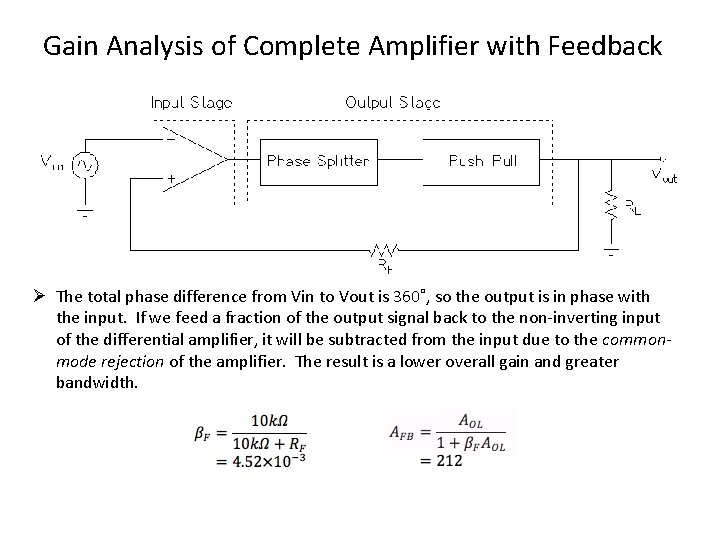
Gain Analysis of Complete Amplifier with Feedback Ø The total phase difference from Vin to Vout is 360˚, so the output is in phase with the input. If we feed a fraction of the output signal back to the non-inverting input of the differential amplifier, it will be subtracted from the input due to the commonmode rejection of the amplifier. The result is a lower overall gain and greater bandwidth.
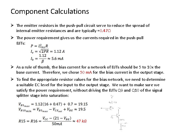
Component Calculations Ø The emitter resistors in the push-pull circuit serve to reduce the spread of internal emitter resistances and are typically ≈0. 47Ω Ø The power requirement gives us the currents required in the push-pull BJTs: Ø As a rule of thumb, the bias current for a network of BJTs should be 5 to 10 x the base current. Therefore, we chose 50 m. A for the bias current in the output stage. Ø To find the appropriate resistor values for the bias network, we need to determine a suitable DC level for the input to the output stage. We want to make sure we satisfy the power requirement, without driving the BJTs Q 9 and Q 10 of the signal splitter stage into saturation:
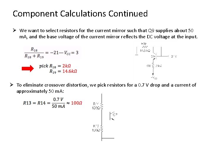
Component Calculations Continued Ø We want to select resistors for the current mirror such that Q 9 supplies about 50 m. A, and the base voltage of the current mirror reflects the DC voltage at the input. Ø To eliminate crossover distortion, we pick resistors for a 0. 7 V drop and a current of approximately 50 m. A:
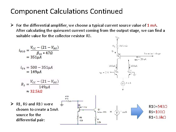
Component Calculations Continued Ø For the differential amplifier, we choose a typical current source value of 1 m. A. After calculating the quiescent current coming from the output stage, we can find a suitable value for the collector resistor R 3. Ø R 1, R 9 and R 10 were chosen to create a 1 m. A source for the differential pair: = R 10=543Ω R 9=100Ω R 1=3. 9 kΩ
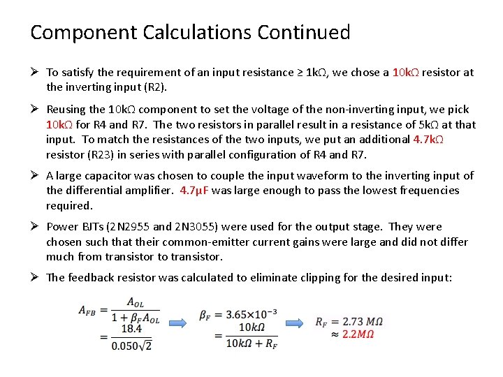
Component Calculations Continued Ø To satisfy the requirement of an input resistance ≥ 1 kΩ, we chose a 10 kΩ resistor at the inverting input (R 2). Ø Reusing the 10 kΩ component to set the voltage of the non-inverting input, we pick 10 kΩ for R 4 and R 7. The two resistors in parallel result in a resistance of 5 kΩ at that input. To match the resistances of the two inputs, we put an additional 4. 7 kΩ resistor (R 23) in series with parallel configuration of R 4 and R 7. Ø A large capacitor was chosen to couple the input waveform to the inverting input of the differential amplifier. 4. 7µF was large enough to pass the lowest frequencies required. Ø Power BJTs (2 N 2955 and 2 N 3055) were used for the output stage. They were chosen such that their common-emitter current gains were large and did not differ much from transistor to transistor. Ø The feedback resistor was calculated to eliminate clipping for the desired input:
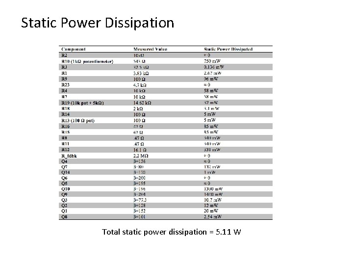
Static Power Dissipation Total static power dissipation = 5. 11 W
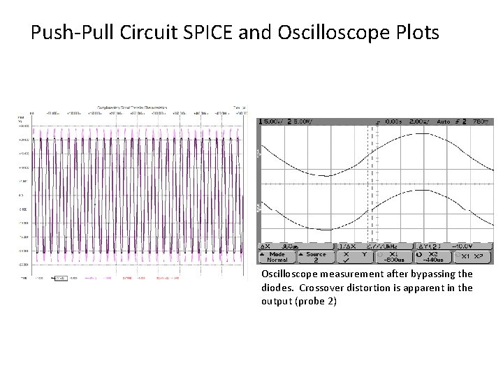
Push-Pull Circuit SPICE and Oscilloscope Plots Oscilloscope measurement after bypassing the diodes. Crossover distortion is apparent in the output (probe 2)
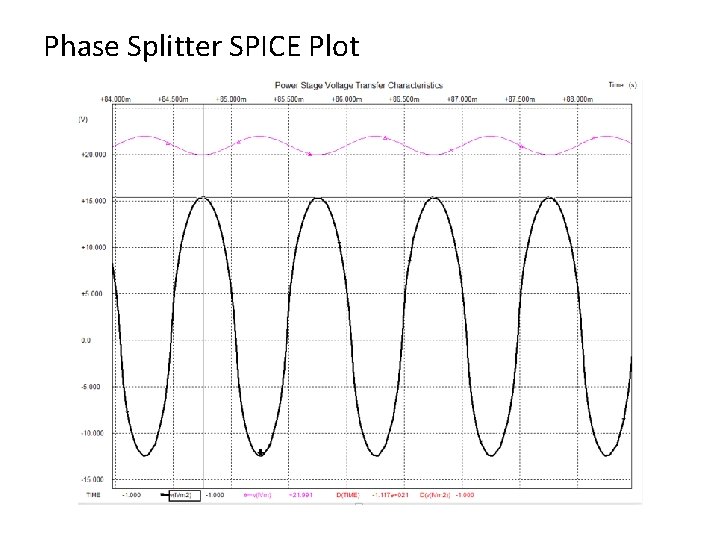
Phase Splitter SPICE Plot
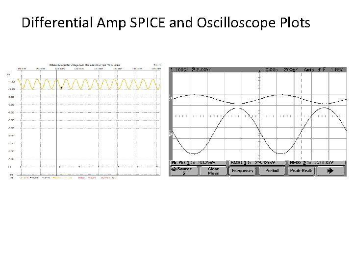
Differential Amp SPICE and Oscilloscope Plots
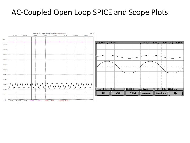
AC-Coupled Open Loop SPICE and Scope Plots
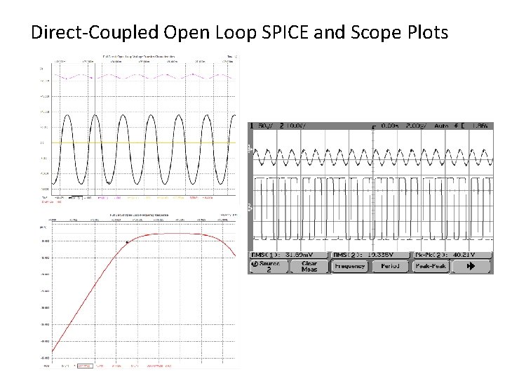
Direct-Coupled Open Loop SPICE and Scope Plots
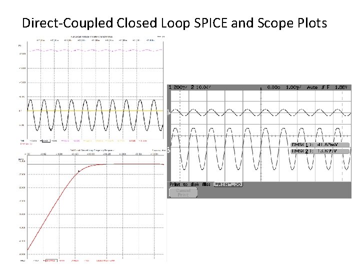
Direct-Coupled Closed Loop SPICE and Scope Plots
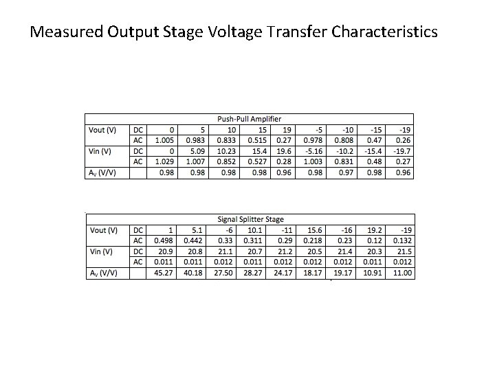
Measured Output Stage Voltage Transfer Characteristics
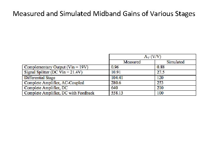
Measured and Simulated Midband Gains of Various Stages
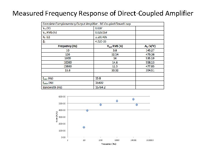
Measured Frequency Response of Direct-Coupled Amplifier
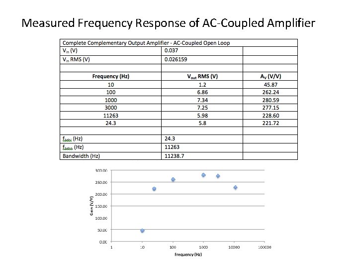
Measured Frequency Response of AC-Coupled Amplifier
Conclusions Ø Large signal amplifiers capable of switching large amounts of current can be built using BJTs and typically include multiple stages, such as a differential stage, a signal splitter and push-pull stage. Ø Unlike common-emitter, common-collector and common-base configurations, a differential amplifier can be directly coupled to an output stage with no loss in gain. Ø Currents in a differential pair must be balanced. If they are not, there might not be sufficient current to allow the output to swing fully in both directions. Ø Bias voltages on either side of a signal splitter and push-pull amplifier must be symmetrical about 0 V to ensure an output voltage of 0 V for an input of 0 V, and to maximize available swing at the output. Ø For best results, the common-emitter current gains of the BJTs on either side of the signal splitter and push-pull amplifier should deviate as little as possible, no more than 5 to 10%.
- Slides: 29