Large area short strip arrays Goal is to















- Slides: 47

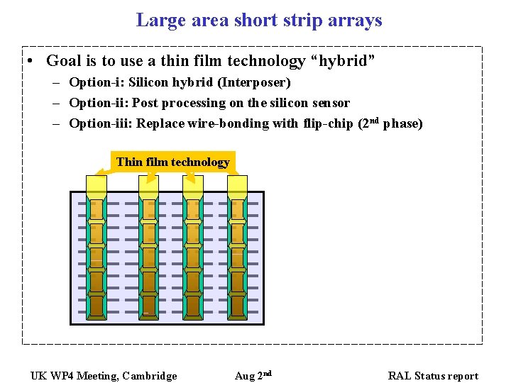
Large area short strip arrays • Goal is to use a thin film technology “hybrid” – Option-i: Silicon hybrid (Interposer) – Option-ii: Post processing on the silicon sensor – Option-iii: Replace wire-bonding with flip-chip (2 nd phase) Thin film technology UK WP 4 Meeting, Cambridge Aug 2 nd RAL Status report

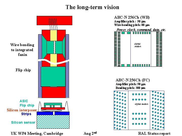
The long-term vision ABC-N 256 Ch (WB) Amplifier pitch : 50 mm Wire-bonding pitch: 80 mm Power, clock, command, data, etc. digital section Wire bonding to integrated fanin Flip chip ABC-N 256 Ch (FC) Amplifier pitch: 50 mm Bonding pitch: 300 mm ASIC Flip chip digital section Silicon interposer Strips Silicon sensor UK WP 4 Meeting, Cambridge Aug 2 nd RAL Status report

Progress report - June/July Review of material estimates for different technologies Interaction with companies (A, I, S) • • • Visit to I (Marc) 2 nd visit to A (Jeff, Lars, Marc) Visit to S (Bob Stevens, CMF) Split project into phases a) b) c) d) e) RD on electrical parameters for sensor post processing Prototyping of a silicon interposer Post processed hybrid – subject to success with a) and b) Flip chip – on hold Integrated silicon cooling – on hold Started on electrical design of hybrid (interposer) – – – Based on US 4 -chip deign (currently working at RAL) Need expert feedback and link into Liverpool work Will invited Wuppertal to RAL to learn more about their post-processed pixel module Investigated Microflex interconnection Updated (more realistic? ) schedule UK WP 4 Meeting, Cambridge Aug 2 nd RAL Status report

Material Estimates (Marc) • Compared – – Ceramic (Be. O) based on Carl’s hybrid Copper-Kapton based on extrapolation from Liverpool A silicon hybrid (= Interposer) using thin-film technology Post processing on sensor • Disclaimer: Many assumptions – – – • ASIC size Hybrid area Metal layer thickness CC bridge, thickness Number of passives (e. g. for decoupling) Thermal heat spreader area… All radiation length estimates are normalized to sensor area UK WP 4 Meeting, Cambridge Aug 2 nd RAL Status report

Material comparisons overview (no base board, no pigtail, no MCC, no SP, see below) SLHC Be. O: 1. 8% R. L. SLHC Copper-Kapton: 1. 4 -1. 9 % R. L. (main uncertainty is thickness of CC bridge) SLHC post-processing: 0. 9 -1% R. L. SLHC silicon interposer: 1 -1. 2% R. L. SCT barrel module: 1. 16 % R. L. (Hybrid: 0. 36%; Sensor: 0. 61%, Baseboard/TPG: 0. 19%) UK WP 4 Meeting, Cambridge Aug 2 nd RAL Status report

Material comparisons details (simplified) This is a condensed version of much more detailed info by Tim, Nobu, Carl and Marc UK WP 4 Meeting, Cambridge Aug 2 nd RAL Status report

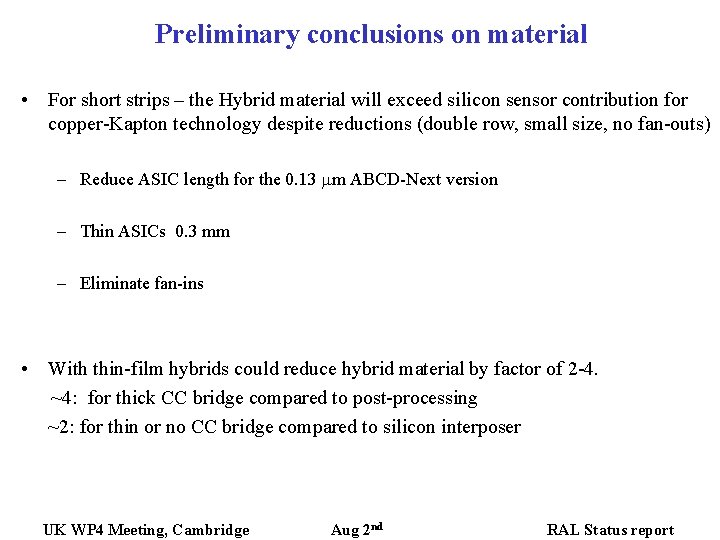
Preliminary conclusions on material • For short strips – the Hybrid material will exceed silicon sensor contribution for copper-Kapton technology despite reductions (double row, small size, no fan-outs) – Reduce ASIC length for the 0. 13 m ABCD-Next version – Thin ASICs 0. 3 mm – Eliminate fan-ins • With thin-film hybrids could reduce hybrid material by factor of 2 -4. ~4: for thick CC bridge compared to post-processing ~2: for thin or no CC bridge compared to silicon interposer UK WP 4 Meeting, Cambridge Aug 2 nd RAL Status report

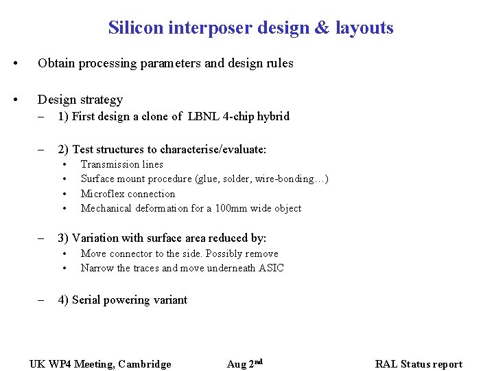
Silicon interposer design & layouts • Obtain processing parameters and design rules • Design strategy – 1) First design a clone of LBNL 4 -chip hybrid – 2) Test structures to characterise/evaluate: • • – 3) Variation with surface area reduced by: • • – Transmission lines Surface mount procedure (glue, solder, wire-bonding…) Microflex connection Mechanical deformation for a 100 mm wide object Move connector to the side. Possibly remove Narrow the traces and move underneath ASIC 4) Serial powering variant UK WP 4 Meeting, Cambridge Aug 2 nd RAL Status report

Processing parameters Info from the 3 companies I, A and CMF are reasonably consistent – Substrate • I: 0. 6 mm, standard high resistivity silicon • A: 4’’ for post-processing on available sensors is OK • 6’’ x ? mmfor silicon interposer (for cost reasons and to look at mechanical issues) – Dielectric: BCB (cyclotene); thickness 5 -15 m • Will get more info on break-through voltages – Metal: • • 1 -5 m Cu (issues are sputtering time and aspect ratios) Minimum trace gap and width: 15 -50 m Electromigration: Max. current density <10 m. A/ um width of copper at 1 m Surface finish: – nickel/gold for aluminium wedge bonding or – nickel/palladium/gold for wedge bonding and soldering – Via diameter: determined by minimum trace width + ~450 opening angle – Number of layers: • A: 4 at 50 m width (additional layers without art-work should be OK) • I: “the less the better” UK WP 4 Meeting, Cambridge Aug 2 nd RAL Status report

Electrical design issues • Geometry & layer thickness of thin-film MCMs require changes in design. • Issues are: – Transmission line impedance (impedances are lower in thin-film; pixel group achieved 50 s rather than the usual ~70 s with low cross talk) – Capacitances. Large capacitances because of thin dielectric help with decoupling but will increase total strip capacitance – Area and thickness of power and ground planes • Why don’t Pixel detectors have ground/power planes? If this is due to much reduced stray capacitances, short strips might make life easier! – High voltage routing and decoupling for detector bias – Attention to Guard ring and silicon edge if silicon extended UK WP 4 Meeting, Cambridge Aug 2 nd RAL Status report

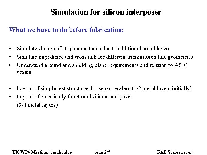
Simulation for silicon interposer What we have to do before fabrication: • Simulate change of strip capacitance due to additional metal layers • Simulate impedance and cross talk for different transmission line geometries • Understand ground and shielding plane requirements and relation to ASIC design • Layout of simple test structures for sensor wafers (1 -2 metal layers initially) • Layout of electrically functional silicon interposer (3 -4 metal layers) UK WP 4 Meeting, Cambridge Aug 2 nd RAL Status report

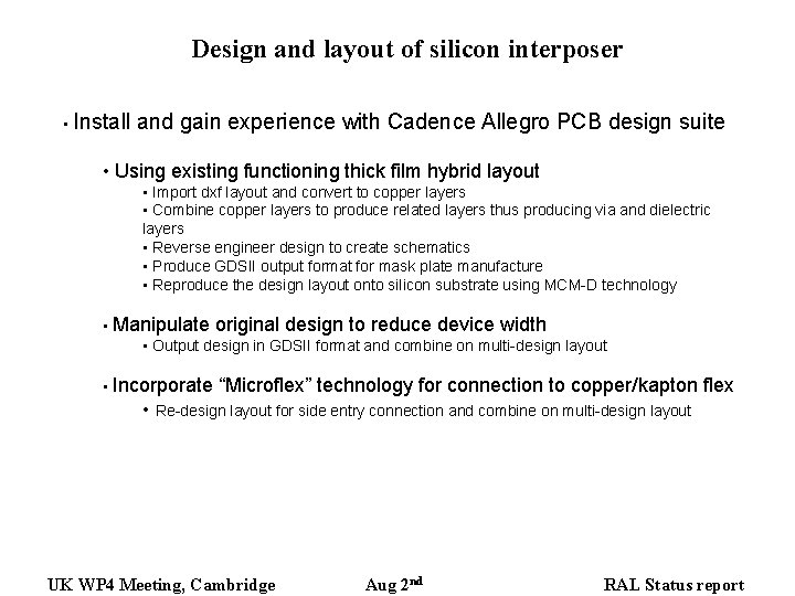
Design and layout of silicon interposer • Install and gain experience with Cadence Allegro PCB design suite • Using existing functioning thick film hybrid layout • Import dxf layout and convert to copper layers • Combine copper layers to produce related layers thus producing via and dielectric layers • Reverse engineer design to create schematics • Produce GDSII output format for mask plate manufacture • Reproduce the design layout onto silicon substrate using MCM-D technology • Manipulate original design to reduce device width • Output design in GDSII format and combine on multi-design layout • Incorporate “Microflex” technology for connection to copper/kapton • Re-design layout for side entry connection and combine on multi-design layout UK WP 4 Meeting, Cambridge Aug 2 nd flex RAL Status report

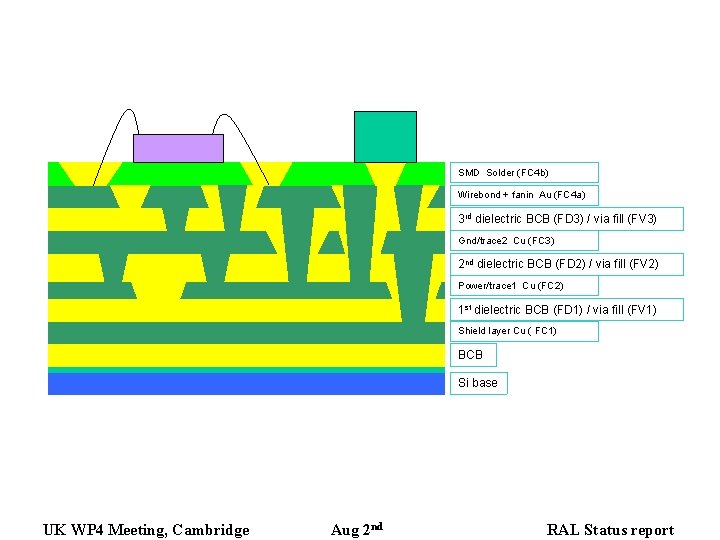
SMD Solder (FC 4 b) Wirebond + fanin Au (FC 4 a) 3 rd dielectric BCB (FD 3) / via fill (FV 3) Gnd/trace 2 Cu (FC 3) 2 nd dielectric BCB (FD 2) / via fill (FV 2) Power/trace 1 Cu (FC 2) 1 st dielectric BCB (FD 1) / via fill (FV 1) Shield layer Cu ( FC 1) BCB Si base UK WP 4 Meeting, Cambridge Aug 2 nd RAL Status report

UK WP 4 Meeting, Cambridge Aug 2 nd RAL Status report

UK WP 4 Meeting, Cambridge Aug 2 nd RAL Status report

UK WP 4 Meeting, Cambridge Aug 2 nd RAL Status report

UK WP 4 Meeting, Cambridge Aug 2 nd RAL Status report

UK WP 4 Meeting, Cambridge Aug 2 nd RAL Status report

UK WP 4 Meeting, Cambridge Aug 2 nd RAL Status report

UK WP 4 Meeting, Cambridge Aug 2 nd RAL Status report

UK WP 4 Meeting, Cambridge Aug 2 nd RAL Status report

UK WP 4 Meeting, Cambridge Aug 2 nd RAL Status report

UK WP 4 Meeting, Cambridge Aug 2 nd RAL Status report

UK WP 4 Meeting, Cambridge Aug 2 nd RAL Status report

UK WP 4 Meeting, Cambridge Aug 2 nd RAL Status report

UK WP 4 Meeting, Cambridge Aug 2 nd RAL Status report

Reduction in area UK WP 4 Meeting, Cambridge Aug 2 nd RAL Status report

35 um How small? • 450 etch angle via to ensure good side wall • No via land so diameter is line width • 15 um dielectric will give 55 um (from 25 um) wide line so should only be used on shield separation layers UK WP 4 Meeting, Cambridge Aug 2 nd 5 um 25 um RAL Status report

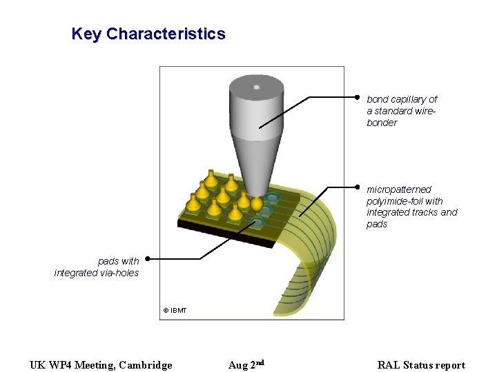
MFI Micro. Flex Interconnection Technology UK WP 4 Meeting, Cambridge Aug 2 nd RAL Status report

Key Characteristics bond capillary of a standard wirebonder micropatterned polyimide-foil with integrated tracks and pads with integrated via-holes © IBMT UK WP 4 Meeting, Cambridge Aug 2 nd RAL Status report

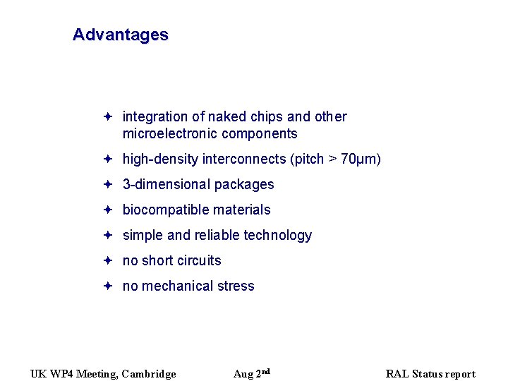
Advantages ª integration of naked chips and other microelectronic components ª high-density interconnects (pitch > 70µm) ª 3 -dimensional packages ª biocompatible materials ª simple and reliable technology ª no short circuits ª no mechanical stress UK WP 4 Meeting, Cambridge Aug 2 nd RAL Status report

Reliability Tests ª biocompatible polyimide foil cytotoxicity tested according to ISO 10993 ª reliable interconnection technology electrical and mechanical tests of the interconnects according to MIL standard 883 test procedure resistance [m ] before and after § temperature cycling -40°C to 150°C in air, 110 h 2. 29 2. 54 § thermal shock -180°C to 100°C in liquids, 100 cycles 2. 04 2. 20 § humidity 95% relative humidity @ 70°C, 110 h 2. 23 2. 08 § high temperature 300°C for 240 h 2. 88 56. 15 § vibration 50 - 2, 000 Hz, gpeak = 20 m/s 2, 48 h 2. 54 1. 70 UK WP 4 Meeting, Cambridge Aug 2 nd RAL Status report

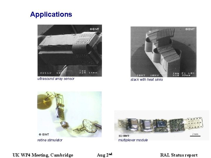
Applications ©IBMT ultrasound array sensor ©IBMT stack with heat sinks © IBMT retina stimulator UK WP 4 Meeting, Cambridge multiplexer module Aug 2 nd RAL Status report

References • Patents: WO 9904453 ‘Contact and method for producing a contact. ’ WO 0207486 ‘Method for producing an electrical and/or mechanical connection between flexible thin-film substrates. ’ • Papers: Stieglitz, T. , Beutel, H. , Meyer, J. -U. : ‘Microflex - A New Assembling Technique for Interconnects’. Journal of Intelligent Material Systems and Structures, 11 (6), pp. 417 -426 (2000). Meyer, J. -U. , Stieglitz, T. , Scholz, O. , Haberer, W. , Beutel, H. : ‘High Density Interconnects and Flexible Hybrid Assemblies for Active Biomedical Implants’. IEEE Trans. on Components, Packaging and Manufacturing Technology-Part B: Advanced Packaging (IEEE Trans. on Advanced Packaging), vol. 24 , no. 3, pp. 366 -374 (2001). UK WP 4 Meeting, Cambridge Aug 2 nd RAL Status report

Post-processing of the Micron wafers • Features of the masks • Test structures • Measurements & simulations UK WP 4 Meeting, Cambridge Aug 2 nd RAL Status report

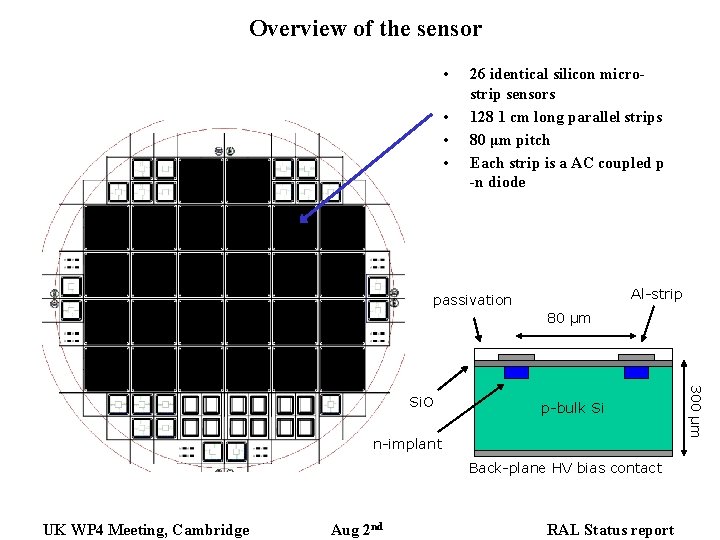
Overview of the sensor • • 26 identical silicon microstrip sensors 128 1 cm long parallel strips 80 μm pitch Each strip is a AC coupled p -n diode Al-strip passivation 80 μm p-bulk Si n-implant Back-plane HV bias contact UK WP 4 Meeting, Cambridge Aug 2 nd RAL Status report 300 μm Si. O

Top view of the micro-strip sensor Serial bias resistors Guard rings (zero field at edge) Strip bond pads HV GND pad Guard ring pads UK WP 4 Meeting, Cambridge Aug 2 nd RAL Status report

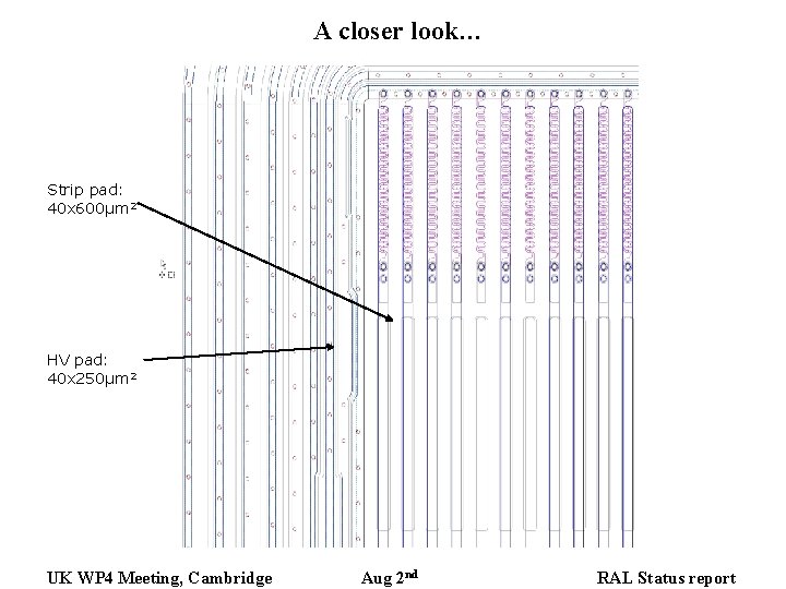
A closer look… Strip pad: 40 x 600μm 2 HV pad: 40 x 250μm 2 UK WP 4 Meeting, Cambridge Aug 2 nd RAL Status report

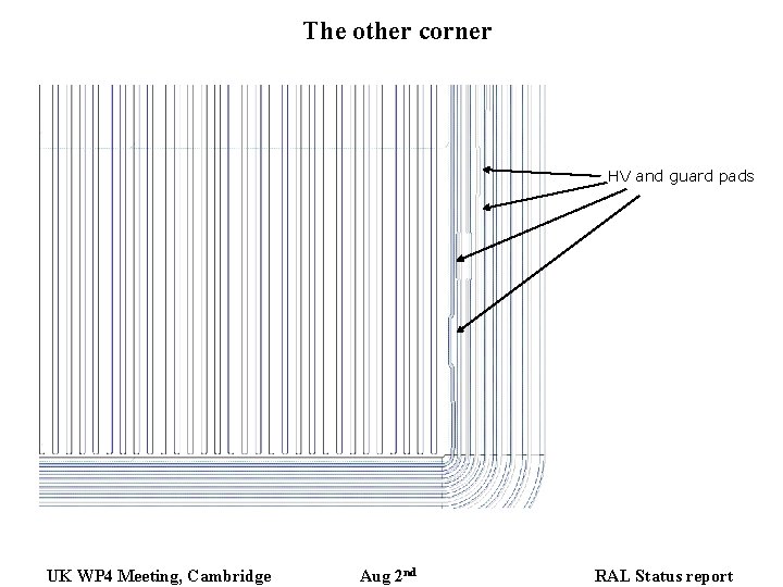
The other corner HV and guard pads UK WP 4 Meeting, Cambridge Aug 2 nd RAL Status report

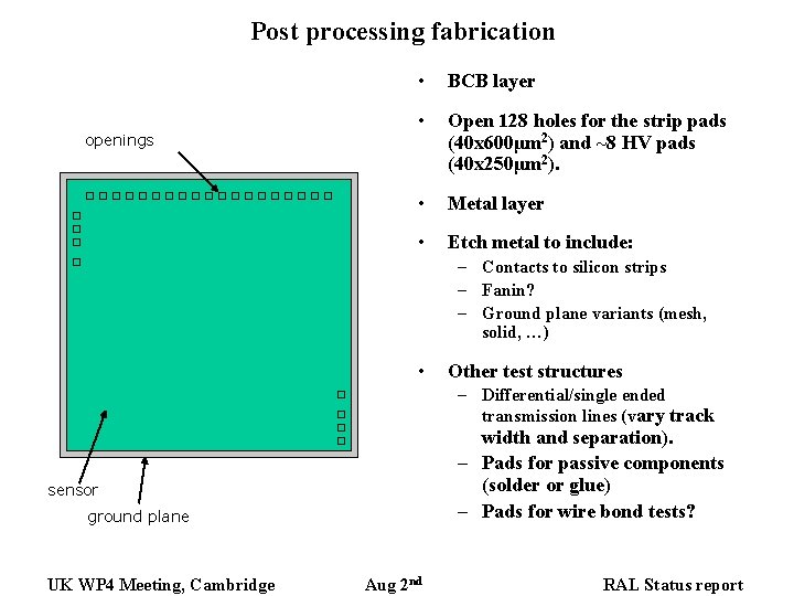
Post processing fabrication openings • BCB layer • Open 128 holes for the strip pads (40 x 600μm 2) and ~8 HV pads (40 x 250μm 2). • Metal layer • Etch metal to include: – Contacts to silicon strips – Fanin? – Ground plane variants (mesh, solid, …) • Other test structures – Differential/single ended transmission lines (vary track width and separation). – Pads for passive components (solder or glue) – Pads for wire bond tests? sensor ground plane UK WP 4 Meeting, Cambridge Aug 2 nd RAL Status report

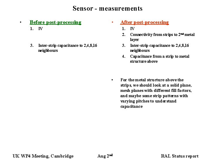
Sensor - measurements • • Before post-processing 1. 2. 3. 4. 1. 2. IV Connectivity from strips to 2 nd metal layer Inter-strip capacitance to 2, 4, 8, 16 neighbours Capacitance from a strip to metal structure above 3. 4. • UK WP 4 Meeting, Cambridge After post-processing Aug 2 nd IV Connectivity from strips to 2 nd metal layer Inter-strip capacitance to 2, 4, 8, 16 neighbours Capacitance from a strip to metal structure above For the metal structure above the strips, we should look at a solid plane, mesh planes with different fill factors, and maybe some strip patterns with varying pitches to understand capacitance RAL Status report

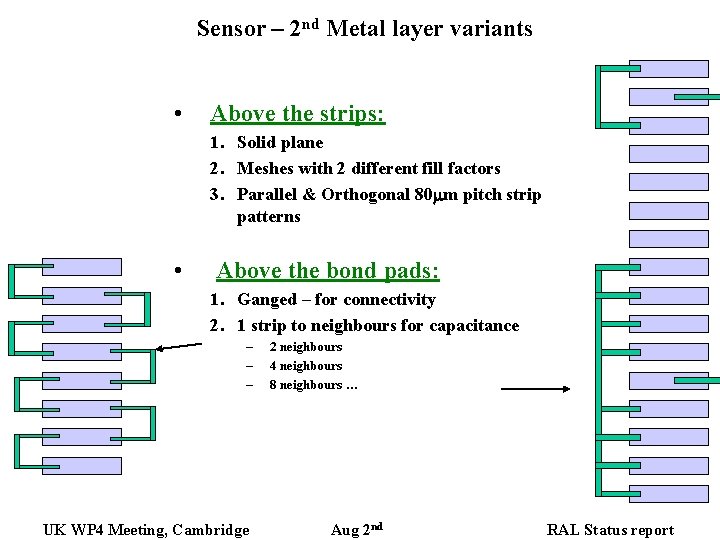
Sensor – 2 nd Metal layer variants • Above the strips: 1. Solid plane 2. Meshes with 2 different fill factors 3. Parallel & Orthogonal 80 mm pitch strip patterns • Above the bond pads: 1. Ganged – for connectivity 2. 1 strip to neighbours for capacitance – – – UK WP 4 Meeting, Cambridge 2 neighbours 4 neighbours 8 neighbours … Aug 2 nd RAL Status report

Open issues • Cu to Al connection • Lithography – no experience with < 50 mm strips • Mechanical stresses & deformation • Detector bias – Routing and decoupling – Non active part of sensor wafer UK WP 4 Meeting, Cambridge Aug 2 nd RAL Status report

Commercial • A are very interested and have supplied a quote; plans have changed a bit so a revision will be required; A have previous experience with thin-film RF designs; they look like a good option. • I will require a 2 nd visit with Jeff, I are interested and have previous experience, their post-processed pixel module had very fine feature sizes and was electrically flawless. Yield was low. • S (UK) is an unknown at this stage but has very good relations with CMF. We will visit them later • Will select the best company or follow a “light” tender exercise to get value for money if more than one option UK WP 4 Meeting, Cambridge Aug 2 nd RAL Status report

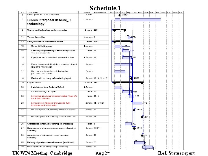
Schedule. 1 UK WP 4 Meeting, Cambridge Aug 2 nd RAL Status report

Schedule. 2 UK WP 4 Meeting, Cambridge Aug 2 nd RAL Status report

Schedule (mpp file) UK WP 4 Meeting, Cambridge Aug 2 nd RAL Status report