Large area ordered Ptype Si nanowire arrays as

- Slides: 1

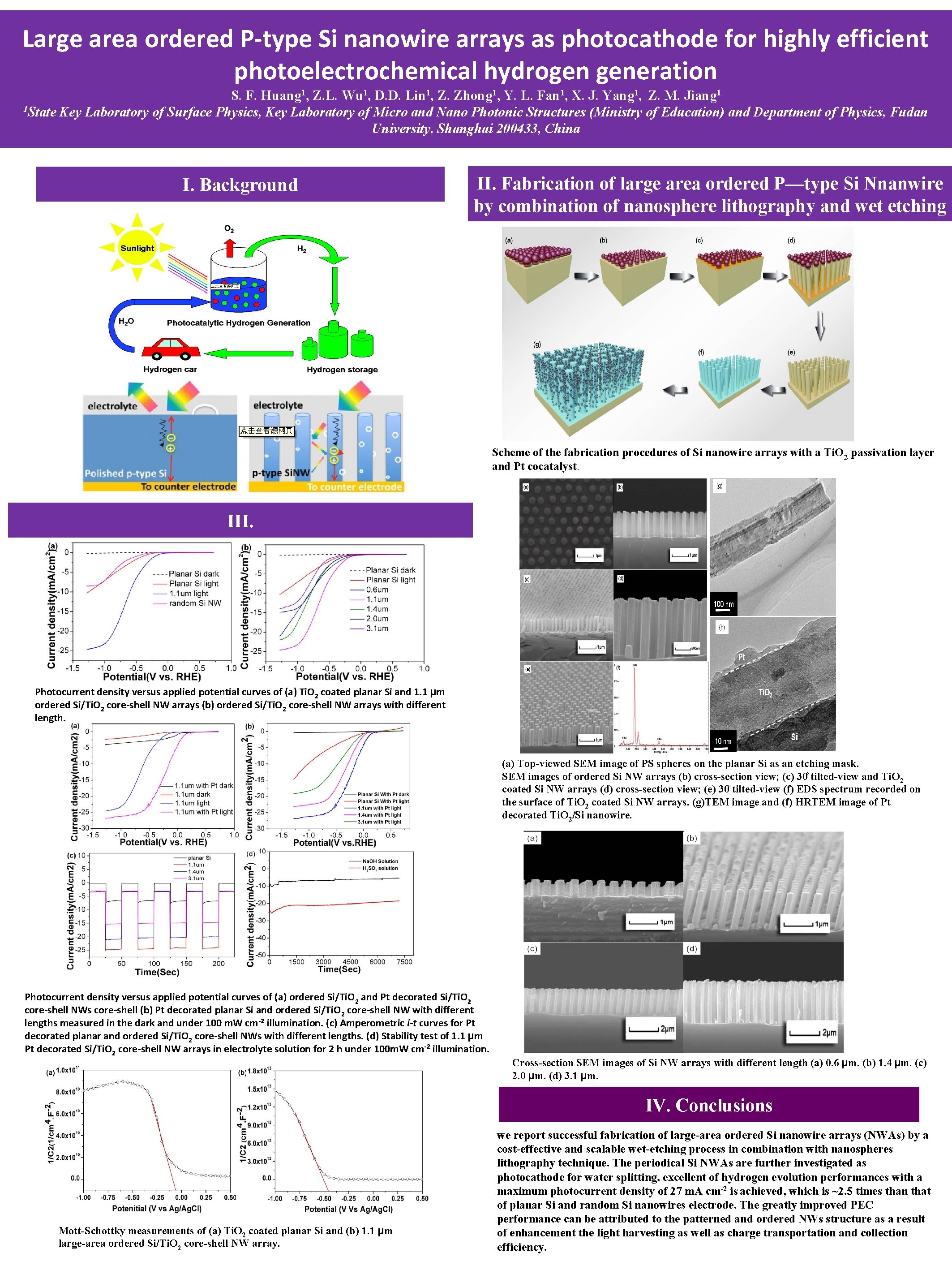
Large area ordered P-type Si nanowire arrays as photocathode for highly efficient photoelectrochemical hydrogen generation S. F. Huang 1, Z. L. Wu 1, D. D. Lin 1, Z. Zhong 1, Y. L. Fan 1, X. J. Yang 1, Z. M. Jiang 1 1 State Key Laboratory of Surface Physics, Key Laboratory of Micro and Nano Photonic Structures (Ministry of Education) and Department of Physics, Fudan University, Shanghai 200433, China I. Background II. Fabrication of large area ordered P—type Si Nnanwire by combination of nanosphere lithography and wet etching Scheme of the fabrication procedures of Si nanowire arrays with a Ti. O 2 passivation layer and Pt cocatalyst. III. Photocurrent density versus applied potential curves of (a) Ti. O 2 coated planar Si and 1. 1 µm ordered Si/Ti. O 2 core-shell NW arrays (b) ordered Si/Ti. O 2 core-shell NW arrays with different length. (a) Top-viewed SEM image of PS spheres on the planar Si as an etching mask. SEM images of ordered Si NW arrays (b) cross-section view; (c) 30 tilted-view and Ti. O 2 coated Si NW arrays (d) cross-section view; (e) 30 tilted-view (f) EDS spectrum recorded on the surface of Ti. O 2 coated Si NW arrays. (g)TEM image and (f) HRTEM image of Pt decorated Ti. O 2/Si nanowire. Photocurrent density versus applied potential curves of (a) ordered Si/Ti. O 2 and Pt decorated Si/Ti. O 2 core-shell NWs core-shell (b) Pt decorated planar Si and ordered Si/Ti. O 2 core-shell NW with different lengths measured in the dark and under 100 m. W cm-2 illumination. (c) Amperometric i-t curves for Pt decorated planar and ordered Si/Ti. O 2 core-shell NWs with different lengths. (d) Stability test of 1. 1 µm Pt decorated Si/Ti. O 2 core-shell NW arrays in electrolyte solution for 2 h under 100 m. W cm -2 illumination. Cross-section SEM images of Si NW arrays with different length (a) 0. 6 µm. (b) 1. 4 µm. (c) 2. 0 µm. (d) 3. 1 µm. IV. Conclusions Mott-Schottky measurements of (a) Ti. O 2 coated planar Si and (b) 1. 1 µm large-area ordered Si/Ti. O 2 core-shell NW array. we report successful fabrication of large-area ordered Si nanowire arrays (NWAs) by a cost-effective and scalable wet-etching process in combination with nanospheres lithography technique. The periodical Si NWAs are further investigated as photocathode for water splitting, excellent of hydrogen evolution performances with a maximum photocurrent density of 27 m. A cm-2 is achieved, which is ~2. 5 times than that of planar Si and random Si nanowires electrode. The greatly improved PEC performance can be attributed to the patterned and ordered NWs structure as a result of enhancement the light harvesting as well as charge transportation and collection efficiency.