Laplace Deep Level Transient Spectroscopy a powerful tool


- Slides: 28

Laplace Deep Level Transient Spectroscopy … a powerful tool for defect analysis in irradiated silicon A. R. Peaker 1, V. Markevich 1, I. D. Hawkins 1, B. Hamilton 1, L. Dobaczewski 2, J. Coutinho 3, R. Jones 4, K. Bonde-Nielsen 5 1 Photon Science Institute, University of Manchester 2 Institute of Physics, Warsaw, Poland 3 I 3 N, University of Aveiro, Portugal 4 Department of Physics, University of Exeter, UK 5 Institute of Physics and Astronomy, University of Århus, Denmark Silicon Radiation Detectors, Manchester 2010

Outline Silicon Radiation Detectors, Manchester 2010

Silicon Radiation Detectors, Manchester 2010

Silicon Radiation Detectors, Manchester 2010

Silicon Radiation Detectors, Manchester 2010

Silicon Radiation Detectors, Manchester 2010

Silicon Radiation Detectors, Manchester 2010

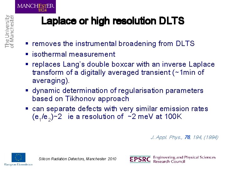
Laplace or high resolution DLTS § removes the instrumental broadening from DLTS § isothermal measurement § replaces Lang’s double boxcar with an inverse Laplace transform of a digitally averaged transient (~1 min of averaging). § dynamic determination of regularisation parameters based on Tikhonov approach § can separate defects with very similar emission rates (e 1/e 2)~2 ie a resolution of ~2 me. V at 100 K J. Appl. Phys. , 76, 194, (1994) Silicon Radiation Detectors, Manchester 2010

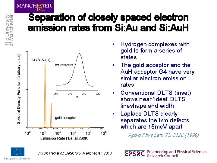
Separation of closely spaced electron emission rates from Si: Au and Si: Au. H • Hydrogen complexes with gold to form a series of states • The gold acceptor and the Au. H acceptor G 4 have very similar electron emission rates • Conventional DLTS (inset) shows near ‘ideal’ DLTS lineshape and width • Laplace DLTS clearly separates the two defects which are 15 me. V apart Appld Phys Lett, 73, 3126 (1998) Silicon Radiation Detectors, Manchester 2010

Laplace or High Resolution DLTS The order of magnitude improvement in energy resolution makes it possible to study aspects of the physics of defects that is not possible by any other techniques but… § sensitivity about an order less than conventional DLTS § the problem of separating exponentials is fundamentally ill posed so result has uncertainty § more difficult to use than conventional DLTS § at the moment only ~50 LDLTS installations worldwide Silicon Radiation Detectors, Manchester 2010 http: //www. laplacedlts. eu

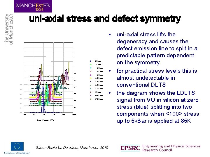
uni-axial stress and defect symmetry 0 kbar 1. 3 kbar 1. 6 kbar 0. 6 1. 9 kbar 2. 2 kbar 0. 5 2. 5 kbar 2. 8 kbar 0. 06 0. 4 0. 05 0. 3 0. 04 0. 03 0. 2 3. 4 kbar 4. 6 kbar 5. 2 kbar 0. 02 0. 1 0. 00 -1. 00 0. 00 1. 00 2. 00 3. 00 4. 000. 0 Z axis: Pressure [GPa] Silicon Radiation Detectors, Manchester 2010 • uni-axial stress lifts the degeneracy and causes the defect emission line to split in a predictable pattern dependent on the symmetry • for practical stress levels this is almost undetectable in conventional DLTS • the diagram shows the LDLTS signal from VO in silicon at zero stress (blue) splitting into two components when <100> stress up to 5 k. Bar is applied at 85 K

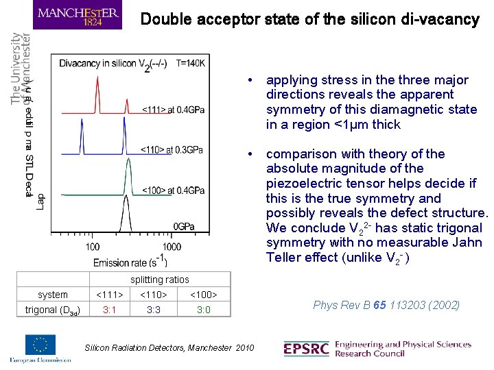
Double acceptor state of the silicon di-vacancy • applying stress in the three major directions reveals the apparent symmetry of this diamagnetic state in a region <1µm thick • comparison with theory of the absolute magnitude of the piezoelectric tensor helps decide if this is the true symmetry and possibly reveals the defect structure. We conclude V 22 - has static trigonal symmetry with no measurable Jahn Teller effect (unlike V 2 - ) splitting ratios system <111> <110> <100> trigonal (D 3 d) 3: 1 3: 3 3: 0 Silicon Radiation Detectors, Manchester 2010 Phys Rev B 65 113203 (2002)

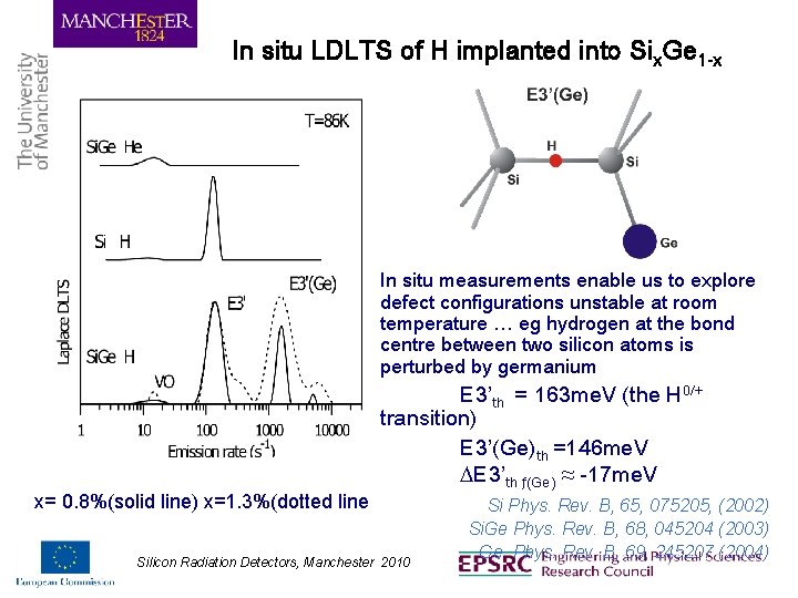
In situ LDLTS of H implanted into Six. Ge 1 -x In situ measurements enable us to explore defect configurations unstable at room temperature … eg hydrogen at the bond centre between two silicon atoms is perturbed by germanium x= 0. 8%(solid line) x=1. 3%(dotted line E 3’th = 163 me. V (the H 0/+ transition) E 3’(Ge)th =146 me. V E 3’th ƒ(Ge) -17 me. V Silicon Radiation Detectors, Manchester 2010 Si Phys. Rev. B, 65, 075205, (2002) Si. Ge Phys. Rev. B, 68, 045204 (2003) Ge Phys. Rev. B, 69, 245207 (2004)

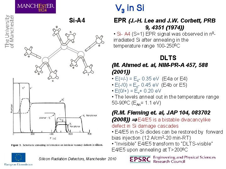
V 3 in Si Si-A 4 EPR (J. -H. Lee and J. W. Corbett, PRB 9, 4351 (1974)) • Si- A 4 (S=1) EPR signal was observed in n 0 irradiated Si after annealing in the temperature range 100 -2500 C DLTS (M. Ahmed et. al, NIM-PR-A 457, 588 (2001)) • E(=/-) = Ec- 0. 35 e. V (E 4 a or E 4) • E(-/0) = Ec- 0. 45 e. V (E 4 b or E 5) • E(0/+) = Ev+ 0. 20 e. V • The levels anneal out in the temperature range 50 -900 C (EAn= 1. 1 e. V) (R. M. Fleming et. al, JAP 104, 083702 (2008)) E 4/E 5 is a bistable divacancylike defect in Si damage cascades • E 4/E 5 in n-Si diodes can be restored by forward bias injection (12 A/cm 2 -20 min-RT) • “Invisible” E 4/E 5 transform to “DLTS-visible” E 4/E 5 upon annealing at T>2000 C Silicon Radiation Detectors, Manchester 2010

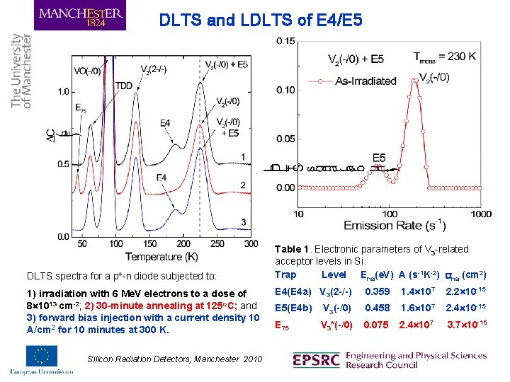
DLTS and LDLTS of E 4/E 5 DLTS spectra for a p+-n diode subjected to: 1) irradiation with 6 Me. V electrons to a dose of 8 1013 cm-2; 2) 30 -minute annealing at 125 o. C; and 3) forward bias injection with a current density 10 A/cm 2 for 10 minutes at 300 K. Silicon Radiation Detectors, Manchester 2010 Table 1. Electronic parameters of V 3 -related acceptor levels in Si. Trap Level Ena(e. V) A (s-1 K-2) na (cm 2) E 4(E 4 a) V 3(2 -/-) 0. 359 1. 4 107 2. 2 10 -15 E 5(E 4 b) V 3(-/0) 0. 458 1. 6 107 2. 4 10 -15 E 75 V 3*(-/0) 0. 075 2. 4 107 3. 7 10 -15

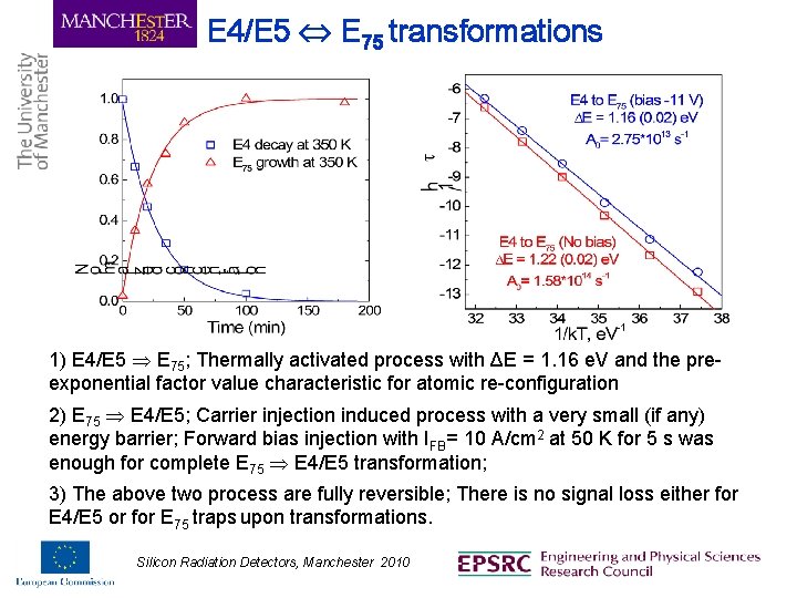
E 4/E 5 E 75 transformations 1) E 4/E 5 E 75; Thermally activated process with ΔE = 1. 16 e. V and the preexponential factor value characteristic for atomic re-configuration 2) E 75 E 4/E 5; Carrier injection induced process with a very small (if any) energy barrier; Forward bias injection with IFB= 10 A/cm 2 at 50 K for 5 s was enough for complete E 75 E 4/E 5 transformation; 3) The above two process are fully reversible; There is no signal loss either for E 4/E 5 or for E 75 traps upon transformations. Silicon Radiation Detectors, Manchester 2010

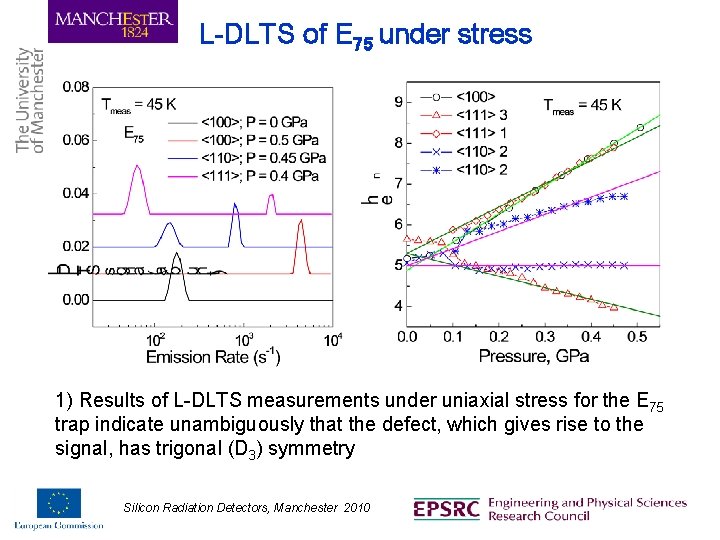
L-DLTS of E 75 under stress 1) Results of L-DLTS measurements under uniaxial stress for the E 75 trap indicate unambiguously that the defect, which gives rise to the signal, has trigonal (D 3) symmetry Silicon Radiation Detectors, Manchester 2010

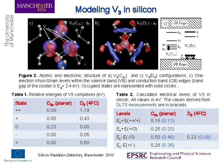
Modeling V 3 in silicon Figure 2. Atomic and electronic structure of a) V 3(C 2 v) and c) V 3(D 3) configurations. c) Oneelectron Khon-Sham levels within the valence band (VB) and conduction band (CB) edges (band gap of the cluster is Eg= 2. 4 e. V). Occupied states are represented with solid circles. Table 1. Relative energies of V 3 complexes (e. V). State ++ C 2 v (planar) 0. 00 D 3 (4 FC) 1. 19 + 0. 00 0. 43 0 0. 23 0. 00 - 0. 00 0. 05 = 0. 00 0. 50 Silicon Radiation Detectors, Manchester 2010 Table 2. Calculated electrical levels of V 3 in silicon. All values in e. V. The values derived from DLTS measurements are in brackets. Levels Ev+E(++/+) C 2 v (planar) 0. 15 (0. 11) Ev+E(+/0) 0. 25 (0. 20) Ec-E(-/0) 0. 50 (0. 46) Ec-E(=/-) 0. 28 (0. 36) D 3 (4 FC) 0. 23 (0. 08)

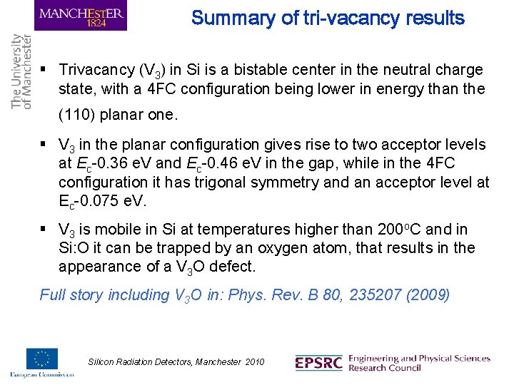
Summary of tri-vacancy results § Trivacancy (V 3) in Si is a bistable center in the neutral charge state, with a 4 FC configuration being lower in energy than the (110) planar one. § V 3 in the planar configuration gives rise to two acceptor levels at Ec-0. 36 e. V and Ec-0. 46 e. V in the gap, while in the 4 FC configuration it has trigonal symmetry and an acceptor level at Ec-0. 075 e. V. § V 3 is mobile in Si at temperatures higher than 200 o. C and in Si: O it can be trapped by an oxygen atom, that results in the appearance of a V 3 O defect. Full story including V 3 O in: Phys. Rev. B 80, 235207 (2009) Silicon Radiation Detectors, Manchester 2010

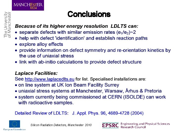
Conclusions Silicon Radiation Detectors, Manchester 2010

Silicon Radiation Detectors, Manchester 2010

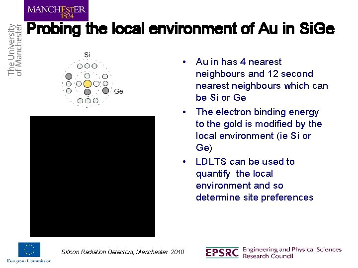
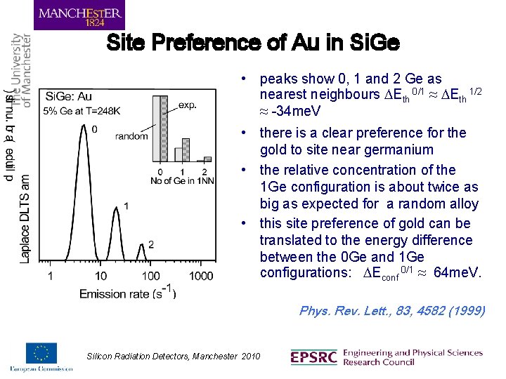
Probing the local environment of Au in Si. Ge • Au in has 4 nearest neighbours and 12 second nearest neighbours which can be Si or Ge • The electron binding energy to the gold is modified by the local environment (ie Si or Ge) • LDLTS can be used to quantify the local environment and so determine site preferences Silicon Radiation Detectors, Manchester 2010

Site Preference of Au in Si. Ge • peaks show 0, 1 and 2 Ge as nearest neighbours Eth 0/1 Eth 1/2 -34 me. V • there is a clear preference for the gold to site near germanium • the relative concentration of the 1 Ge configuration is about twice as big as expected for a random alloy • this site preference of gold can be translated to the energy difference between the 0 Ge and 1 Ge configurations: Econf 0/1 64 me. V. Phys. Rev. Lett. , 83, 4582 (1999) Silicon Radiation Detectors, Manchester 2010

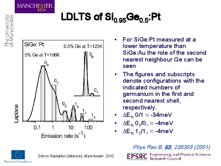
LDLTS of Si 0. 95 Ge 0. 5: Pt • For Si. Ge: Pt measured at a lower temperature than Si. Ge: Au the role of the second nearest neighbour Ge can be seen • The figures and subscripts denote configurations with the indicated numbers of germanium in the first and second nearest shell, respectively. • Eth 0/1 -34 me. V • Eth 00/01 -4 me. V • Eth 10/11 -4 me. V Phys Rev B, 63, 235309 (2001) Silicon Radiation Detectors, Manchester 2010

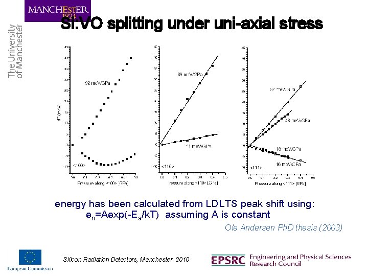
Si: VO splitting under uni-axial stress energy has been calculated from LDLTS peak shift using: en=Aexp(-Ea/k. T) assuming A is constant Ole Andersen Ph. D thesis (2003) Silicon Radiation Detectors, Manchester 2010

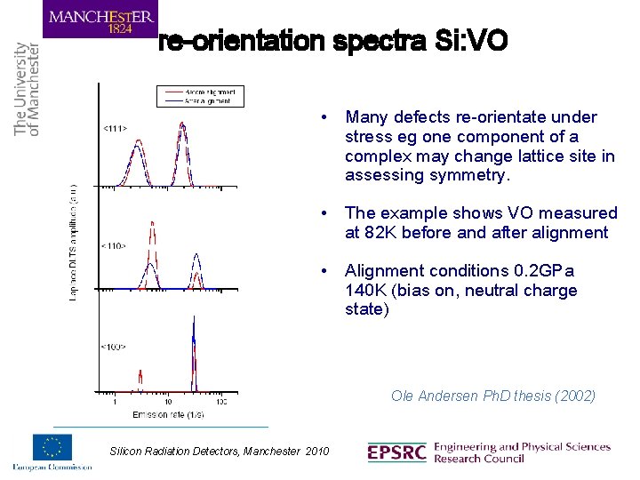
re-orientation spectra Si: VO • Many defects re-orientate under stress eg one component of a complex may change lattice site in assessing symmetry. • The example shows VO measured at 82 K before and after alignment • Alignment conditions 0. 2 GPa 140 K (bias on, neutral charge state) Ole Andersen Ph. D thesis (2002) Silicon Radiation Detectors, Manchester 2010

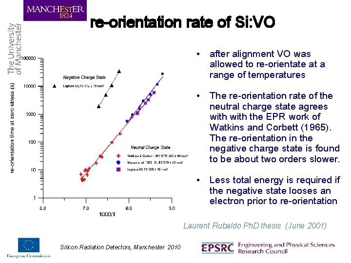
re-orientation rate of Si: VO • after alignment VO was allowed to re-orientate at a range of temperatures • The re-orientation rate of the neutral charge state agrees with the EPR work of Watkins and Corbett (1965). The re-orientation in the negative charge state is found to be about two orders slower. • Less total energy is required if the negative state looses an electron prior to re-orientation Laurent Rubaldo Ph. D thesis (June 2001) Silicon Radiation Detectors, Manchester 2010

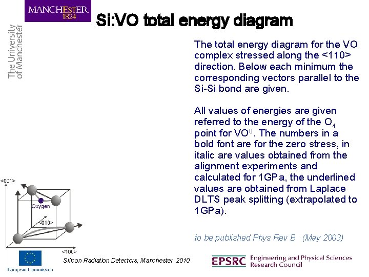
Si: VO total energy diagram The total energy diagram for the VO complex stressed along the <110> direction. Below each minimum the corresponding vectors parallel to the Si-Si bond are given. All values of energies are given referred to the energy of the O 4 point for VO 0. The numbers in a bold font are for the zero stress, in italic are values obtained from the alignment experiments and calculated for 1 GPa, the underlined values are obtained from Laplace DLTS peak splitting (extrapolated to 1 GPa). to be published Phys Rev B (May 2003) Silicon Radiation Detectors, Manchester 2010