
LABORATORI NAZIONALI DI FRASCATI www lnf infn it
LABORATORI NAZIONALI DI FRASCATI www. lnf. infn. it The µ-RWELL technology G. Bencivenni, LNF – INFN
OUTLINE q Muon detectors for future colliders q The micro-RWELL q The performance q Future perspectives & Summary 2
Muon Detectors for future colliders q The future colliders (Cep. C, Spp. C and FCC – hh) requires for extremely large muon detectors : q ~10000 m 2 in the barrel q 3 -5000 m 2 in the end-cap q 300 m 2 in the very forward region q The detectors have to be operated in high background environment (very large uncertainties depending on shielding, actual structure, etc. ): q O(1 – 10 k. Hz/cm 2) in the barrel q O(10 – 100 k. Hz/cm 2) in the end-cap q O(1 MHz/cm 2) in the forward region q Taking into account the surface and the expected rates gaseous detectors and in particular MPGDs is the natural solution (for Cep. C, as well as for Spp. C, FCC-ee and FCC-hh) q R&D for HL-LHC (CMS & LHCb phase-2 muon upgrade) could be clearly a good starting point
Why a new MPGD The R&D on µ-RWELL is mainly motivated by the wish of improving the stability under heavy irradiation & simplify as much as possible construction/assembly procedures
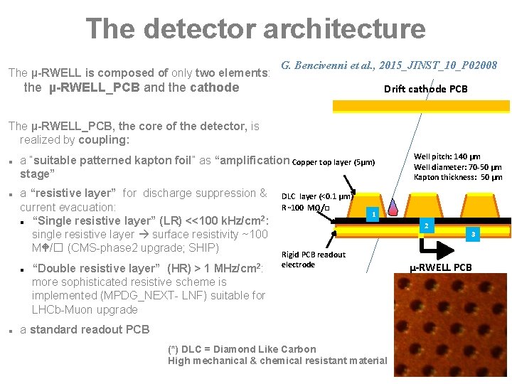
The detector architecture The µ-RWELL is composed of only two elements: G. Bencivenni et al. , 2015_JINST_10_P 02008 the µ-RWELL_PCB and the cathode Drift cathode PCB The µ-RWELL_PCB, the core of the detector, is realized by coupling: a “suitable patterned kapton foil” as “amplification Copper top layer (5µm) stage” a “resistive layer” for discharge suppression & current evacuation: 2 “Single resistive layer” (LR) <<100 k. Hz/cm : single resistive layer surface resistivity ~100 M /☐ (CMS-phase 2 upgrade; SHIP) “Double resistive layer” (HR) > 1 MHz/cm 2: more sophisticated resistive scheme is implemented (MPDG_NEXT- LNF) suitable for LHCb-Muon upgrade DLC layer (<0. 1 µm) R 100 MΩ/□ Well pitch: 140 µm Well diameter: 70 -50 µm Kapton thickness: 50 µm 1 2 Rigid PCB readout electrode a standard readout PCB (*) DLC = Diamond Like Carbon High mechanical & chemical resistant material 5 3 µ-RWELL PCB
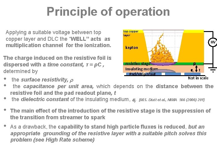
Principle of operation Applying a suitable voltage between top copper layer and DLC the “WELL” acts as multiplication channel for the ionization. The charge induced on the resistive foil is dispersed with a time constant, τ = ρC , determined by • • • top copper layer HV kapton resistive stage Insulating medium Pad/strip r/out r t Not in scale the surface resistivity, the capacitance per unit area, which depends on the distance between the resistive foil and the pad readout plane, t the dielectric constant of the insulating medium, r [M. S. Dixit et al. , NIMA 566 (2006) 281] The main effect of the introduction of the resistive stage is the suppression of the transition from streamer to spark As a drawback, the capability to stand high particle fluxes is reduced, but an appropriate grounding of the resistive layer with a suitable pitch solves this problem (see High Rate scheme)
Technology features The µ-RWELL is a single-amplification stage, intrinsically spark protected MPGD characterized by: • simple assembly procedure: • • cost effective: • • only two components µ-RWELL_PCB + cathode no critical & time consuming assembly steps: • no gluing • no stretching ( no stiff & large frames needed) • easy handling suitable for large area with PCB splicing technique w/small dead zone 1 PCB r/o, 1 µ-RWELL foil, 1 DLC, 1 cathode and very low man-power easy to operate: • very simple HV supply only 2 independent HV channels or a trivial passive divider (while 3 GEM detector 7 HV floating/channels )
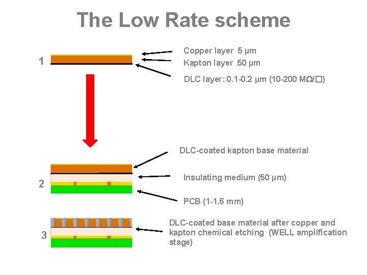
The Low Rate scheme Copper layer 5 µm 1 Kapton layer 50 µm DLC layer: 0. 1 -0. 2 µm (10 -200 M /☐) DLC-coated kapton base material 2 Insulating medium (50 µm) PCB (1 -1. 6 mm) 3 DLC-coated base material after copper and kapton chemical etching (WELL amplification stage)
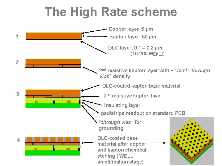
The High Rate scheme Copper layer 5 µm 1 Kapton layer 50 µm DLC layer: 0. 1 – 0. 2 µm (10 -200 M /☐) 2 2 nd resistive kapton layer with ∼ 1/cm 2 “through vias” density DLC-coated kapton base material 3 2 nd resistive kapton layer insulating layer pad/strips readout on standard PCB “through vias” for grounding 4 DLC-coated base material after copper and kapton chemical etching ( WELL amplification stage)
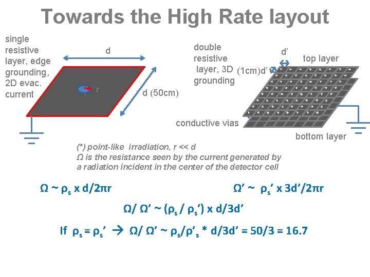
Towards the High Rate layout single resistive layer, edge grounding, 2 D evac. current double resistive layer, 3 D (1 cm)d’ grounding d r r d’ top layer d (50 cm) conductive vias bottom layer (*) point-like irradiation, r << d Ω is the resistance seen by the current generated by a radiation incident in the center of the detector cell Ω ~ ρs x d/2πr Ω’ ~ ρs’ x 3 d’/2πr Ω/ Ω’ ~ (ρs / ρs’) x d/3 d’ If ρs = ρs’ Ω/ Ω’ ~ ρs/ρ’s * d/3 d’ = 50/3 = 16. 7
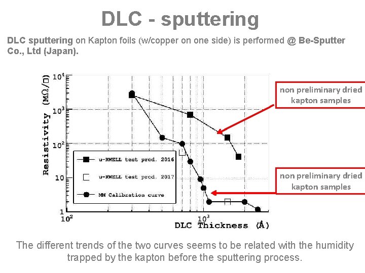
DLC - sputtering DLC sputtering on Kapton foils (w/copper on one side) is performed @ Be-Sputter Co. , Ltd (Japan). non preliminary dried kapton samples The different trends of the two curves seems to be related with the humidity trapped by the kapton before the sputtering process.
2017 R&D Program I. Technology Transfer to ELTOS of the single-layer (large area - CMS) PCBRWELL manufacturing: in progress w/good results (final kapton etching still at CERN) II. Technology Transfer to TECHTRA for the etching of the amplification-stage (kapton etching): just started (tuning the procedure … ) III. Ageing Test @ GIF++ of large area single-layer RWELL + small area doublelayer (v 1. 0) RWELL: in progress (till end of the year) IV. Construction of prototypes based on double-layer layout + an alternative simplified scheme: 10 x 10 cm 2 with pad size of 0. 6 x 0. 8 cm 2 V. Test Beam @ H 4 -SPS (5 – 19 Jul) : efficiency/cluster-size (pad r/o) studies VI. Test Beam @ PSI (4 – 18 Dec - tbc) with a high intensity hadron beam in current mode: - rate capability with a particle flux up to 20 MHz/cm 2 - discharge probability - integrating a charge equivalent to some years of operation @ HL Colliders ?
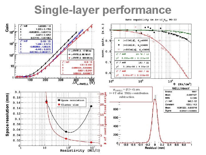
Space resolution (mm) Single-layer performance RWELL = (52+-6) µm @ B= 0 T after TRKs contribution subtraction
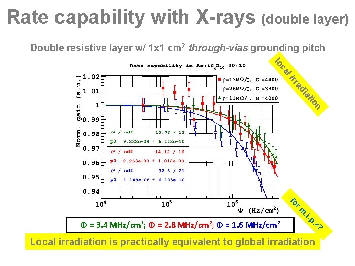
Rate capability with X-rays (double layer) Double resistive layer w/ 1 x 1 cm 2 through-vias grounding pitch li ca lo a rr n io at di rm fo. i. × 7 p. Φ = 3. 4 MHz/cm 2; Φ = 2. 8 MHz/cm 2; Φ = 1. 6 MHz/cm 2 Local irradiation is practically equivalent to global irradiation
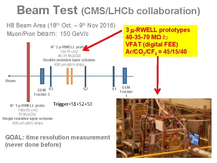
Beam Test (CMS/LHCb collaboration) H 8 Beam Area (18 th Oct. – 9 th Nov 2016) Muon/Pion beam: 150 Ge. V/c N° 2 µ-RWELL protos 10 x 10 cm 2 40 -35 M /☐� Double resistive layer scheme 400 µm pitch strips 3 -RWELL prototypes 40 -35 -70 MΩ /□ VFAT (digital FEE) Ar/CO 2/CF 4 = 45/15/40 Beam GEM S 3 Tracker 2 S 2 Trigger=S 1+S 2+S 3 N° 1 µ-RWELL proto 100 x 50 cm 2 70 M /☐� Single resistive layer scheme 800 µm pitch strips GOAL: time resolution measurement (never done before) S 1 GEM Tracker 1
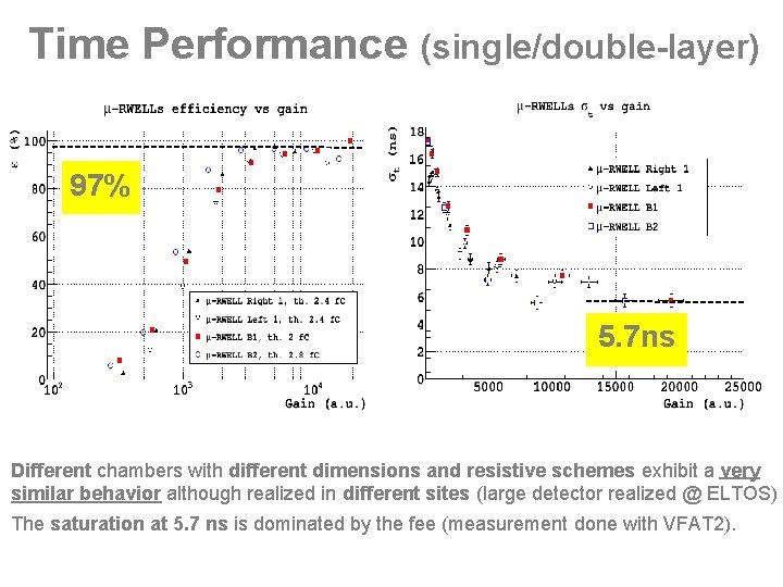
Time Performance (single/double-layer) 97% 5. 7 ns Different chambers with different dimensions and resistive schemes exhibit a very similar behavior although realized in different sites (large detector realized @ ELTOS) The saturation at 5. 7 ns is dominated by the fee (measurement done with VFAT 2).
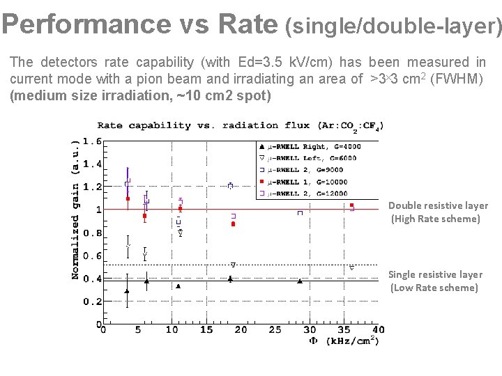
Performance vs Rate (single/double-layer) The detectors rate capability (with Ed=3. 5 k. V/cm) has been measured in current mode with a pion beam and irradiating an area of >3ˣ 3 cm 2 (FWHM) (medium size irradiation, ~10 cm 2 spot) Double resistive layer (High Rate scheme) Single resistive layer (Low Rate scheme)
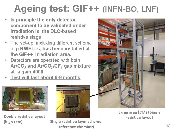
Ageing test: GIF++ (INFN-BO, LNF) • In principle the only detector component to be validated under irradiation is the DLC-based resistive stage. • The set-up, including different scheme of µ-RWELLs, has been installed at the GIF++ irradiation area. • Detectors are operated with both Ar/CO 2 and Ar/CO 2/CF 4 gas mixture at a gain 4000 • Test will last about 6 -9 months Double resistive layout (high rate) Single resistive layer scheme (reference chamber) Large area (CMS) Single resistive layout 18
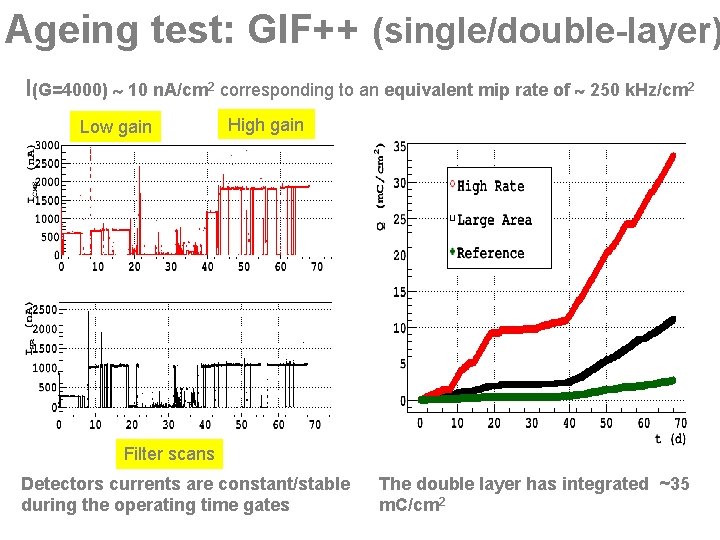
Ageing test: GIF++ (single/double-layer) I(G=4000) 10 n. A/cm 2 corresponding to an equivalent mip rate of 250 k. Hz/cm 2 Low gain High gain Filter scans Detectors currents are constant/stable during the operating time gates The double layer has integrated ~35 m. C/cm 2
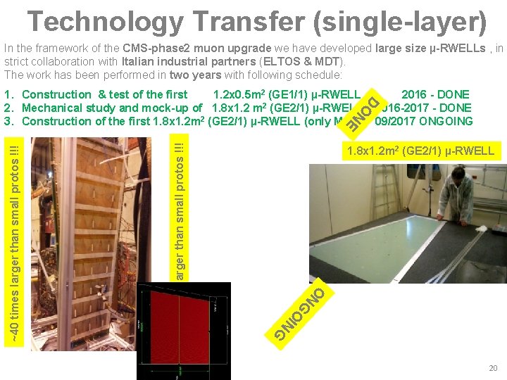
Technology Transfer (single-layer) In the framework of the CMS-phase 2 muon upgrade we have developed large size µ-RWELLs , in strict collaboration with Italian industrial partners (ELTOS & MDT). The work has been performed in two years with following schedule: O NG G ~200 times larger than small protos !!! 1. 8 x 1. 2 m 2 (GE 2/1) µ-RWELL O IN ~40 times larger than small protos !!! 2016 - DONE 2016 -2017 - DONE 09/2017 ONGOING DO NE 1. Construction & test of the first 1. 2 x 0. 5 m 2 (GE 1/1) µ-RWELL 2. Mechanical study and mock-up of 1. 8 x 1. 2 m 2 (GE 2/1) µ-RWELL 3. Construction of the first 1. 8 x 1. 2 m 2 (GE 2/1) µ-RWELL (only M 4) 20
2018 R&D program (very preliminary) I. Technology Transfer to ELTOS for PCB-RWELL manufacturing + TECHTRA for amplification-stage (kapton) etching, with construction of prototypes II. ENGINEERING of the HIGH RATE layout (double layer or other simplified scheme) with construction of prototypes III. Test Beam @ H 4(H 8)-SPS for prototypes characterization IV. Test Beam @ PSI with high intensity hadron beam in current mode (in case of no confirmation of the Dec-2017 TB slot) RD_FA RWELL-Group composition (preliminary): G. Bencivenni (20%), G. Felici, M. Gatta, G. Morello, M. Poli Lener … a MAECI project has been recently submitted: “Design, Industrialization and Production of an innovative Micro Pattern Gas Detector (MPGD) based on the micro-RWELL technology“
COLLABORATION OF SEVERAL INFN (/RD_FA) GROUPS: - BARI - BOLOGNA - FERRARA - FRASCATI - TORINO Global budget of the project: 465500 k€ INFN co-funding (w/salary): 185000 k€ INFN (RD_FA, CMS, BESIII): 40000 k€ MAECI: 240500 k€
SUMMARY The µ-RWELL is a compact, single-amplification stage, simple to assemble & suitable for large area muon apparata, MPGD: ü gas gain > 104 ü intrinsically spark protected ü rate capability >> 1 MHz/cm 2 (HR version) ü space resolution ∼ 60µm ü time resolution ∼ 5. 7 ns R&D/engineering (RD_FA task): o Low rate (<100 k. Hz/cm 2 – Cep. C, FCC-ee) : • small and large area prototypes built and extensively tested • Technological Transfer to industry is ongoing o High rate (>1 MHz/cm 2 - Spp. S, FCC-hh): • first prototypes show promising performance • the engineering still to be started
- Slides: 23