Lab 3 FPGA Implementation Specification RTL design and

Lab 3: FPGA Implementation Specification RTL design and Simulation Logic Synthesis Gate Level Simulation ASIC Layout FPGA Implementation 1 張明峰 交大資 系 Lab 3 -1

Why Top-Down? • Design of complex systems • Reduce time-to-market – shorten the design verification loop – focus on functionality • Easier and cheaper to explore different design option 2 張明峰 交大資 系 Lab 3 -2

RTL Design • Characteristics – fully clock driven RTL code with some behavioral constructs – contain complete functional description – cycle accurate • Coding style – structural description (component connections/net-list) – data flow description (continuous assignment) – RTL description (always block) • combinational RTL • sequential RTL 3 張明峰 交大資 系 Lab 3 -3
 begin")
Logic Synthesis • Translate synthesizable RTL code to gate-level design Always @(posedge clk) begin if(sel 1) begin if(sel 2) out = in 1 ; else out = in 2 ; else if(sel 3) if(sel 4) out = in 3 ; else out = in 4 ; endmodule Gate-level circuits 4 張明峰 交大資 系 Lab 3 -4

Structural Mapping 5 張明峰 交大資 系 Lab 3 -5
 r=a+c; else r=a+b; • Sharing – a")
Resource Sharing • Example if (op_code ==0) r=a+c; else r=a+b; • Sharing – a single ALU for the two additions – a MUX for the second input of the ALU • No-Sharing – two adders for the two additions – an output MUX to select the output 6 張明峰 交大資 系 Lab 3 -6

Register Inferencing • Determines which signals must be preserved across cycle boundaries – incomplete logic specification (missing branches) – explicit register instantiation • always @(posedge clk) – signal used before assigned 7 張明峰 交大資 系 Lab 3 -7

Two-level Logic Optimization • AND-OR representations – – – easy implementation as PLAs and PLDs a key optimization technique efficient algorithms and heuristics exist in commercial use for several years minimize the number of product terms • Example – F = XYZ + XY’Z’ + XY’Z + X’YZ + XYZ – F = XY’ + YZ 8 張明峰 交大資 系 Lab 3 -8

Multi-Level Logic Optimization • Meet performance or area constraints through restructuring and simplifications – two-level minimization – common factor extraction – common expression re-substitution • Trade-off between area and delay • In commercial use for several years – f 1 = abcd+abce+ab’cd’+ab’c’d+a’c+cdf+abc’d’e’+ab’c’df’ – f 2 = bdg + b’dfg + b’d’g+bd’eg – f 1 = c(a’+x)+ac’x’ – f 2 = gx – x = d(b+f) + d’(b’+e) 9 張明峰 交大資 系 Lab 3 -9

Transformation Examples • Algebraic Factoring F = A C D + A B C + ABC + ACD G = 16 – Factoring: F = A( C D + B C ) + A (BC + CD ) G = 16 – Factoring again: F = A C( B + D ) + AC (B + D ) G = 12 – Factoring again: F = ( A C+ AC) (B + D) G = 10 10 張明峰 交大資 系 Lab 3 -10

Transformation Examples • Decomposition – The terms B + D and AC + AC can be defined as new functions E and H respectively, decomposing F: F = E H, E = B + D , and H =AC + AC G = 10 • This series of transformations has reduced G from 16 to 10, a substantial savings. The resulting circuit has three levels plus input inverters. 11 張明峰 交大資 系 Lab 3 -11

Transformation Examples • Substitution of E into F – Returning to F just before the final factoring step: F = A C ( B + D ) + AC (B + D ) G = 12 – Defining E = B + D , and substituting in F: F = A C E + ACE G = 10 – This substitution has resulted in the same cost as the decomposition 12 張明峰 交大資 系 Lab 3 -12

Transformation Examples • Elimination – Beginning with a new set of functions: X=B+C Y=A+B Z = AX + C Y G = 10 – Eliminating X and Y from Z: Z = A (B + C) + C (A + B) G = 10 – “Flattening” (Converting to SOP expression): Z = A B + A C + AC + BC G = 12 – This has increased the cost, but has provided an new SOP expression for two-level optimization. 13 張明峰 交大資 系 Lab 3 -13

Transformation Examples • Two-level Optimization – The result of 2 -level optimization is: Z= AB+ C G=4 • This example illustrates that: – Optimization can begin with any set of equations, not just with minterms or a truth table – Increasing gate input count G temporarily during a series of transformations can result in a final solution with a smaller G 14 張明峰 交大資 系 Lab 3 -14

Transformation Examples • Extraction – Beginning with two functions: E = A B D + A BD H = B C D + BCD G = 16 – Finding a common factor and defining it as a function: F = BD + BD – We perform extraction by expressing E and H as the three functions: F = BD + BD, E = A F, H = CF G = 10 – The reduced cost G results from the sharing of logic between the two output functions 15 張明峰 交大資 系 Lab 3 -15

Technology Mapping • Translation of a technology independent representation of a circuit into a circuit in a given technology with optimal cost • Optimization criteria – – minimum area minimum delay meeting specified timing constraints with minimum area • Usages – Technology mapping after technology independent logic optimization 16 張明峰 交大資 系 Lab 3 -16

Sample covers 17 張明峰 交大資 系 Lab 3 -17

State Machine Synthesis • Translate state table or graph – state minimization – state assignment to minimize the cost function • Challenges – – state machine decomposition state assignment for performance state assignment for testability extract state graph from implementation 18 張明峰 交大資 系 Lab 3 -18

Spartan II Features u Plentiful logic and memory resources – 15 K to 200 K system gates (up to 5, 292 logic cells) – Up to 57 Kb block RAM storage u Flexible I/O interfaces – From 86 to 284 I/Os – 16 signal standards u u Advanced 0. 25/0. 22 um 6 -Layer Metal Process High performance – System frequency as high as 200 MHz u u u Advanced Clock Control with 4 Dedicated DLLs Unlimited Re-programmability Fully PCI Compliant 19 張明峰 交大資 系 Lab 3 -19

Spartan-II Top-level Architecture • Configurable logic blocks – Implement logic here! • I/O blocks – Communicate with other chips – Choose from 16 signal standards • Block RAM – On-chip memory for higher performance 20 張明峰 交大資 系 Lab 3 -20

Spartan-II Top-level Architecture • Clocks and delay locked loops – Synchronize to clock on and off chip • Rich interconnect resources – Three-state internal buses • Power down mode – Lower quiescent power 21 張明峰 交大資 系 Lab 3 -21
 • 1 CLB holds 2 slices • Each slice contains two")
CLB Slice (Simplified) • 1 CLB holds 2 slices • Each slice contains two sets of the following: – Four-input LUT • Any 4 -input logic function • Or 16 -bit x 1 RAM • Or 16 -bit shift register 22 張明峰 交大資 系 Lab 3 -22
 • Each slice contains two sets of the following: – Carry")
CLB Slice (cont’d) • Each slice contains two sets of the following: – Carry & control • Fast arithmetic logic • Multiplier logic • Multiplexer logic – Storage element • • Latch or flip-flop Set and reset True or inverted inputs Sync. or async. control 23 張明峰 交大資 系 Lab 3 -23

Dedicated Expansion Multiplexers • MUXF 5 combines 2 LUTs to form – 4 x 1 multiplexer – Or any 5 -input function CL B Slice • MUXF 6 combines 2 slices to form LUT – 8 x 1 multiplexer – Or any 6 -input function LUT MUXF 6 MUXF 5 Slice LUT MUXF 5 24 張明峰 交大資 系 Lab 3 -24
 • Registered input, output, 3 -state control • Programmable slew rate,")
I/O Block (Simplified) • Registered input, output, 3 -state control • Programmable slew rate, pull-up, pull-down, keeper and input delay 張明峰 交大資 系 Lab 3 -25

I/O Interface Standards • I/O can be programmed for 16 different signal standards – VCCO controls maximum output swing – VREF sets input, output, three-state control • Different banks can support different standards at the same time – Logic level translation – Boards with mixed standards 張明峰 交大資 系 Lab 3 -26

IOBs Organized As Independent Banks • As many as eight banks on a device – Package dependent • Each bank can be assigned any of the 16 signal standards • XC 2 S 50 – – GCK 0: pin 80 GCK 1: pin 77 GCK 2: pin 182 GCK 3: pin 185 張明峰 交大資 系 Lab 3 -27

High Performance Routing • Hierarchical routing • Sparse connections on longer interconnects for high speed • Routing delay depends primarily on distance 2 ns s 2 n – Direction independent – Device-size independent 2 ns – Singles, hexes, longs • Predictable for early design analysis CLB Array 28 張明峰 交大資 系 Lab 3 -28

Power-down Mode • • Controlled by single power down pin All inputs blocked, appear low internally All outputs disabled All register states preserved Power-down status pin Synchronous wake up 100 u. A typical 29 張明峰 交大資 系 Lab 3 -29

Configuration Modes There are four ways to program a Spartan-II FPGA 30 張明峰 交大資 系 Lab 3 -30

Spartan-II Family Overview 31 張明峰 交大資 系 Lab 3 -31

Spartan-II Architecture Summary u Delivers all the key requirements for ASIC replacement – – – – 200, 000 gates 200 MHz Flexible I/O interfaces On-chip distributed and block RAM Clock management Low power Complete development system support 32 張明峰 交大資 系 Lab 3 -32

Xilinx ISE 8 • Integrated Software Environment 33 張明峰 交大資 系 Lab 3 -33

Foundation Project Manager • Integrates all tools into one environment 34 張明峰 交大資 系 Lab 3 -34

Schematic Entry 35 張明峰 交大資 系 Lab 3 -35

State Machine Graphical Editor w. Graphical editor synthesizes into ABEL or VHDL code 張明峰 交大資 系 36 Lab 3 -36

Simulation - Easy to Use and Learn • Generate stimulus easily and quickly – Keyboard toggling – Simple clock stimulus – Custom formulas • Easy debugging – Waveform viewer – Signals easily added and removed – Simulator access from schematic – Color-coded values on schematic • Script Editor 37 張明峰 交大資 系 Lab 3 -37

What is Implementation? • More than just “Place & Route” • Implementation includes many phases – Translate: Merge multiple design files into a single netlist – Map: Group logical symbols from the netlist (gates) into physical components (CLBs and IOBs) – Place & Route: Place components onto the chip, connect them, and extract timing data into reports – Timing (Sim): Generate a back-annotated netlist for timing simulation tools – Configure: Generate a bitstream for device configuration 38 張明峰 交大資 系 Lab 3 -38

Terminology • Project – Source file; has a defined working directory and family • Version – A Xilinx netlist translation of the schematic – Multiple Versions result from iterative schematic changes • Revision – An implementation of a Xilinx netlist – Multiple revisions typically result from different options • Part type – Specified at translation; can be changed in a new revision 39 張明峰 交大資 系 Lab 3 -39

Starting the Flow Engine Foundation Project Manager 40 張明峰 交大資 系 Lab 3 -40

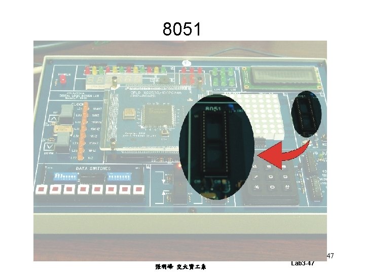
LP-2900 -XC 2 S 50 PQ 208 41 張明峰 交大資 系 Lab 3 -41

FPGA – XC 2 S 50 42 張明峰 交大資 系 Lab 3 -42

Data Switches 43 張明峰 交大資 系 Lab 3 -43

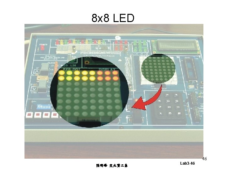
7 -segment & LED 44 張明峰 交大資 系 Lab 3 -44

Keyboard 45 張明峰 交大資 系 Lab 3 -45

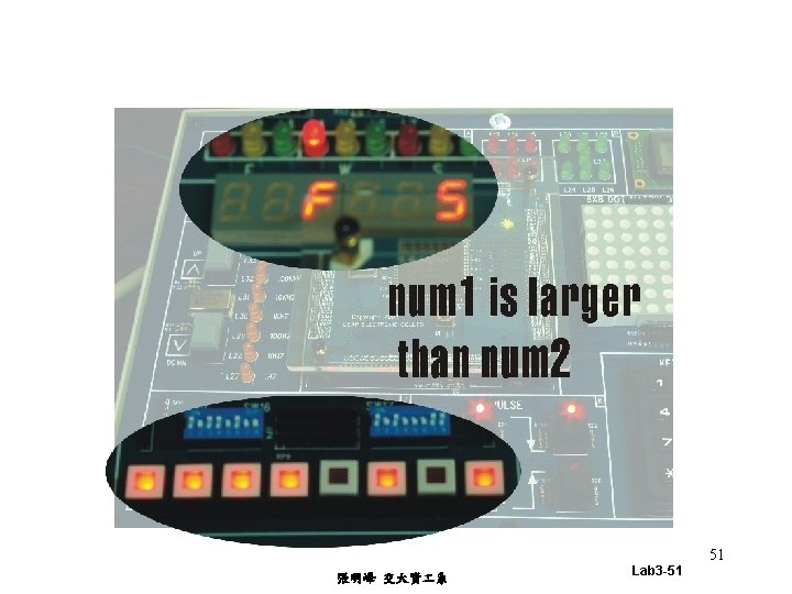
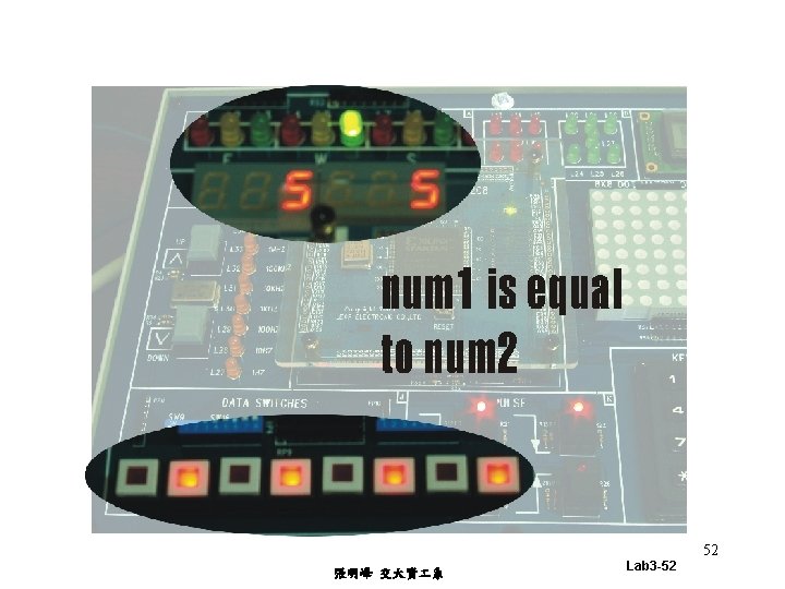
Lab 3: 7 -Segment Display & LED • Input: two 4 -bit numbers num 1, num 2 ( push buttons sw 1~sw 8 ) • Show the number in 7 -Segment Display(active high) • Compare num 1 and num 2, Use LED to show the result ( LED 4 = 1 when num 1 > num 2; LED 6 = 1 when num 1 == num 2; LED 8 = 1 when num 1 < num 2 ) 48 張明峰 交大資 系 Lab 3 -48
![{agb, alb, aeb}=3’b 001 7485 SW[1: 4] 7 -seg dec. SW[5: 8] 7 -seg](http://slidetodoc.com/presentation_image/293353f382a56387a07171bdbb75e341/image-49.jpg "{agb, alb, aeb}=3’b 001 7485 SW[1: 4] 7 -seg dec. SW[5: 8] 7 -seg")
{agb, alb, aeb}=3’b 001 7485 SW[1: 4] 7 -seg dec. SW[5: 8] 7 -seg dec. agbo albo aebo 49 張明峰 交大資 系 Lab 3 -49

Example 50 張明峰 交大資 系 Lab 3 -50
- Slides: 52