Lab 2 ModuleBased Digital Circuit Design and Verification

Lab 2 Module-Based Digital Circuit Design and Verification 1
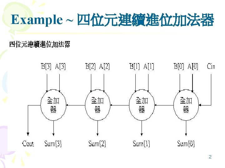
 3")
Example (cont. ) 3

Full Adder 4
 v. Select Tool Check schematic and no error and Save.")
Full Adder (cont. ) v. Select Tool Check schematic and no error and Save. 1 2 5
 v. Select Tool Symbol Wizard 2 1 3 6")
Full Adder (cont. ) v. Select Tool Symbol Wizard 2 1 3 6
 1 2 7")
Full Adder (cont. ) 1 2 7
 v. Finish. 1 8")
Full Adder (cont. ) v. Finish. 1 8

Create New Schematic 2 Right Click v Select “New Source” and type “ser_adder” under the File name. v Cilick next and finish. 3 4 1 5 檔名開頭請勿使用數字或特殊符號 並不要使用中文為檔名 6 9
 v See “ser_adder” in the project and you can")
Create New Schematic (cont. ) v See “ser_adder” in the project and you can use “fulladder” in the symbols. 2 3 1 10
 1 Right Click 2 3 11")
Example (cont. ) 1 Right Click 2 3 11
 v. To complete circuit. 12")
Example (cont. ) v. To complete circuit. 12
 v. Select Tool Check schematic and no error and Save. 1")
Example (cont. ) v. Select Tool Check schematic and no error and Save. 1 2 13
 v You can see the schematic hierarchy and start to simulation,")
Example (cont. ) v You can see the schematic hierarchy and start to simulation, so select “New Source” to add test bench wave. 2 Right Click 3 1 14
 v. Type “ser_adder_tb” under the File name. 1 2 檔名開頭請勿使用數字或特殊符號 並不要使用中文為檔名")
Example (cont. ) v. Type “ser_adder_tb” under the File name. 1 2 檔名開頭請勿使用數字或特殊符號 並不要使用中文為檔名 6 3 4 5 15
 v Modify the ser_adder_tb. v and save it. 16")
Example (cont. ) v Modify the ser_adder_tb. v and save it. 16
 v. Select “Behavioral” and Run. 1 2. Right Click 3 17")
Example (cont. ) v. Select “Behavioral” and Run. 1 2. Right Click 3 17
 v. Select Run-all. 18")
Example (cont. ) v. Select Run-all. 18

Combine Signal 1 MSB LSB 2 Select Signal 19
![Combine Signal [1] 1 2 3 20](http://slidetodoc.com/presentation_image_h/ba23671801571cd56f2d0740d348e9cf/image-20.jpg "Combine Signal [1] 1 2 3 20")
Combine Signal [1] 1 2 3 20
![Combine Signal [2] 1. Right Click 2 3 21](http://slidetodoc.com/presentation_image_h/ba23671801571cd56f2d0740d348e9cf/image-21.jpg "Combine Signal [2] 1. Right Click 2 3 21")
Combine Signal [2] 1. Right Click 2 3 21
![Combine Signal [3] 2 MSB 1 3 LSB 22](http://slidetodoc.com/presentation_image_h/ba23671801571cd56f2d0740d348e9cf/image-22.jpg "Combine Signal [3] 2 MSB 1 3 LSB 22")
Combine Signal [3] 2 MSB 1 3 LSB 22

Result 23

Question & Answer 24
- Slides: 24