Lab 2 Basic Gates in a PLD Module

Lab 2 Basic Gates in a PLD Module M 2. 3 Section 4. 2 Experiment 2 (p. 63)

Experiment 2
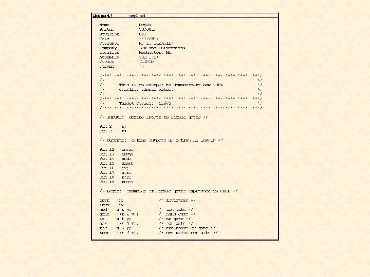

CUPL Header

CUPL Comments

CUPL Inputs and Outputs

CUPL Logic Equations

CUPL Chip Diagram in. DOC File

Fuse Plot for !X

Structure of the GAL 16 V 8 PLD

Fuse Plot for !Y

Structure of the GAL 16 V 8 PLD

Fuse Plot for X & Y

Structure of the GAL 16 V 8 PLD
")
Fuse Plot for !(X & Y)

GAL 16 V 8 Polarity Control OE A C Pin B Polarity X X closed B = 0 open B = 1 C=A C = !A

Fuse Plot for X & Y
")
Fuse Plot for !(X & Y)

Fuse Plot for X # Y

Structure of the GAL 16 V 8 PLD
")
Fuse Plot for !(X # Y)

Fuse Plot for X $ Y

Structure of the GAL 16 V 8 PLD
")
Fuse Plot for !(X $ Y)

JEDEC File

JEDEC File Header

JEDEC File Fuse Map

Experiment 2 Basic Gates • Modify the file, Exp 2. pld, by using pins 6 and 7 for the two inputs X and Y respectively. • Modify the simulation file, Exp 2. si on the web to use your header. • Compile the program using Win. Cupl and run the simulation. • Print out the chip diagram from the. DOC file. • Print out the fuse maps. • Program the GAL 16 V 8 chip.
 and 7 (Y) to Out")
Experiment 2 Basic Gates • Connect pins 6 (X) and 7 (Y) to Out 1 and Out 0. • Connect pins 12 -15 to In 4 -In 1. Print the truth table. Label each output column with the appropriate gate. • Connect pins 16 -19 to In 4 -In 1. Print the truth table. Label each output column with the appropriate gate. • Explain the fuse maps.
- Slides: 29