L 27 Datapath RISCV CPU Datapath Control Intro
![L 27: Datapath CMPT 295 Implementing R-Types Reg[] +4 pc IMEM inst[11: 7] Addr. L 27: Datapath CMPT 295 Implementing R-Types Reg[] +4 pc IMEM inst[11: 7] Addr.](https://slidetodoc.com/presentation_image_h2/86a5aee15f20d703de19c8fcaf545326/image-7.jpg)
![L 27: Datapath CMPT 295 Adding addi to datapath Reg[] +4 Data. D pc+4 L 27: Datapath CMPT 295 Adding addi to datapath Reg[] +4 Data. D pc+4](https://slidetodoc.com/presentation_image_h2/86a5aee15f20d703de19c8fcaf545326/image-8.jpg)
![L 27: Datapath CMPT 295 Current Datapath +4 wb pc+4 pc IMEM inst[11: 7] L 27: Datapath CMPT 295 Current Datapath +4 wb pc+4 pc IMEM inst[11: 7]](https://slidetodoc.com/presentation_image_h2/86a5aee15f20d703de19c8fcaf545326/image-11.jpg)
![L 27: Datapath CMPT 295 Adding sw to datapath +4 pc wb IMEM Reg[] L 27: Datapath CMPT 295 Adding sw to datapath +4 pc wb IMEM Reg[]](https://slidetodoc.com/presentation_image_h2/86a5aee15f20d703de19c8fcaf545326/image-12.jpg)
- Slides: 17

L 27: Datapath RISC-V CPU Datapath, Control Intro CMPT 295

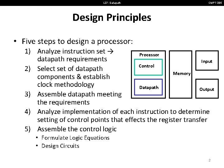
L 27: Datapath CMPT 295 Design Principles • Five steps to design a processor: 1) Analyze instruction set → Processor datapath requirements Input Control 2) Select set of datapath Memory components & establish clock methodology Datapath Output 3) Assemble datapath meeting the requirements 4) Analyze implementation of each instruction to determine setting of control points that effects the register transfer 5) Assemble the control logic • Formulate Logic Equations • Design Circuits 2

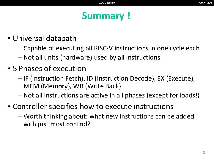
L 27: Datapath CMPT 295 Summary ! • Universal datapath − Capable of executing all RISC-V instructions in one cycle each − Not all units (hardware) used by all instructions • 5 Phases of execution − IF (Instruction Fetch), ID (Instruction Decode), EX (Execute), MEM (Memory), WB (Write Back) − Not all instructions are active in all phases (except for loads!) • Controller specifies how to execute instructions − Worth thinking about: what new instructions can be added with just most control? 3

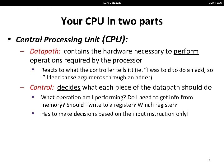
L 27: Datapath CMPT 295 Your CPU in two parts • Central Processing Unit (CPU): – Datapath: contains the hardware necessary to perform operations required by the processor • Reacts to what the controller tells it! (ie. “I was told to do an add, so I”ll feed these arguments through an adder) – Control: decides what each piece of the datapath should do • What operation am I performing? Do I need to get info from • memory? Should I write to a register? Which register? Has to make decisions based on the input instruction only! 4

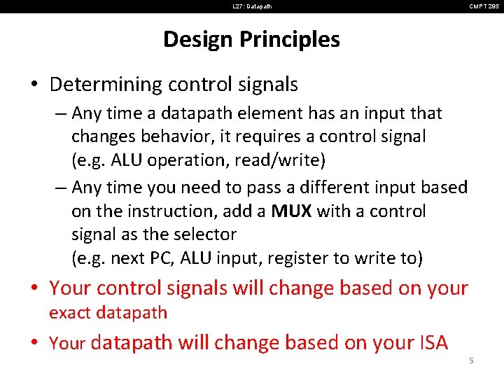
L 27: Datapath CMPT 295 Design Principles • Determining control signals – Any time a datapath element has an input that changes behavior, it requires a control signal (e. g. ALU operation, read/write) – Any time you need to pass a different input based on the instruction, add a MUX with a control signal as the selector (e. g. next PC, ALU input, register to write to) • Your control signals will change based on your exact datapath • Your datapath will change based on your ISA 5

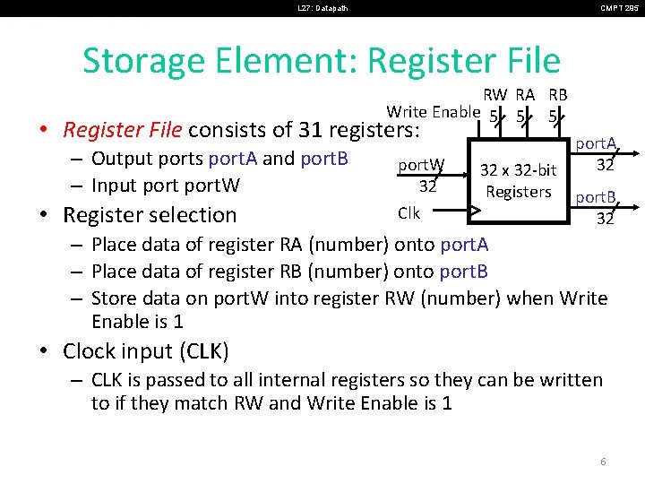
L 27: Datapath CMPT 295 Storage Element: Register File RW RA RB Write Enable 5 5 5 • Register File consists of 31 registers: – Output ports port. A and port. B – Input port. W • Register selection port. W 32 Clk 32 x 32 -bit Registers port. A 32 port. B 32 – Place data of register RA (number) onto port. A – Place data of register RB (number) onto port. B – Store data on port. W into register RW (number) when Write Enable is 1 • Clock input (CLK) – CLK is passed to all internal registers so they can be written to if they match RW and Write Enable is 1 6
![L 27 Datapath CMPT 295 Implementing RTypes Reg 4 pc IMEM inst11 7 Addr L 27: Datapath CMPT 295 Implementing R-Types Reg[] +4 pc IMEM inst[11: 7] Addr.](https://slidetodoc.com/presentation_image_h2/86a5aee15f20d703de19c8fcaf545326/image-7.jpg)
L 27: Datapath CMPT 295 Implementing R-Types Reg[] +4 pc IMEM inst[11: 7] Addr. D inst[19: 15] Addr. A Data. A inst[24: 20] Addr. B Data. B R[rs 1] ALU R[rs 2] inst[31: 0] ALUSel (4) Perform operation - New hardware: ALU (Arithmetic Logic Unit) - Abstraction for adders, multipliers, dividers, etc. - How do we know what operation to execute? - Our first control bit! ALUSel(ect) Control 7
![L 27 Datapath CMPT 295 Adding addi to datapath Reg 4 Data D pc4 L 27: Datapath CMPT 295 Adding addi to datapath Reg[] +4 Data. D pc+4](https://slidetodoc.com/presentation_image_h2/86a5aee15f20d703de19c8fcaf545326/image-8.jpg)
L 27: Datapath CMPT 295 Adding addi to datapath Reg[] +4 Data. D pc+4 pc IMEM inst[11: 7] Reg[rs 1 inst[19: 15] Addr. A Data. A ] Reg[rs inst[24: 20] Addr. B Data. B 2] inst[31: 20] inst[31: 0] ALU Addr. D Imm. Gen 0 1 Also works for all other Iformat arithmetic instruction (slti, sltiu, andi, ori, xori, slli, srai) just by changing ALUSel imm[31: 0] Imm. Sel=I Reg. WEn=1 Control Logic alu BSel=1 ALUSel=Add 8

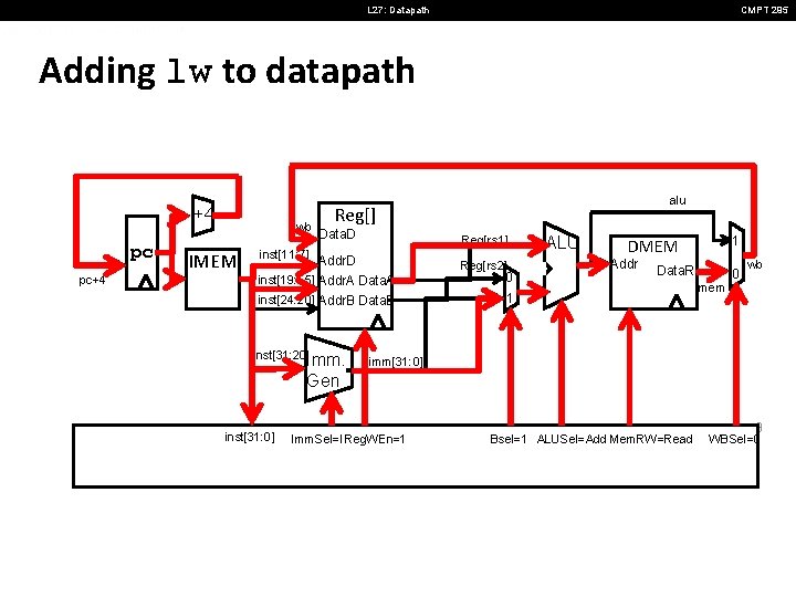
L 27: Datapath CMPT 295 Adding lw to datapath +4 pc pc+4 wb IMEM alu Reg[] Data. D Reg[rs 1] inst[11: 7] Addr. D Reg[rs 2] inst[19: 15] Addr. A Data. A 0 inst[24: 20] Addr. B Data. B 1 inst[31: 20] Imm. Gen inst[31: 0] ALU 1 DMEM Addr Data. R mem 0 wb imm[31: 0] Imm. Sel=I Reg. WEn=1 Bsel=1 ALUSel=Add Mem. RW=Read 9 WBSel=0

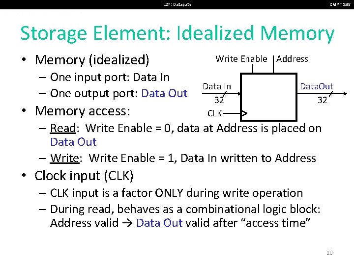
L 27: Datapath CMPT 295 Storage Element: Idealized Memory • Memory (idealized) – One input port: Data In – One output port: Data Out • Memory access: Write Enable Address Data In 32 CLK Data. Out 32 – Read: Write Enable = 0, data at Address is placed on Data Out – Write: Write Enable = 1, Data In written to Address • Clock input (CLK) – CLK input is a factor ONLY during write operation – During read, behaves as a combinational logic block: Address valid → Data Out valid after “access time” 10
![L 27 Datapath CMPT 295 Current Datapath 4 wb pc4 pc IMEM inst11 7 L 27: Datapath CMPT 295 Current Datapath +4 wb pc+4 pc IMEM inst[11: 7]](https://slidetodoc.com/presentation_image_h2/86a5aee15f20d703de19c8fcaf545326/image-11.jpg)
L 27: Datapath CMPT 295 Current Datapath +4 wb pc+4 pc IMEM inst[11: 7] ALU Reg[] Data. D ALU Reg[rs 1] Addr. D Reg[rs 2] Addr inst[19: 15] Addr. A Data. A 0 inst[24: 20] Addr. B Data. B 1 inst[31: 20]Imm. Gen inst[31: 0] Imm. Sel 1 DMEM Data. R 0 wb mem imm[31: 0] BSel ALUSel Mem. RW WBSel 11
![L 27 Datapath CMPT 295 Adding sw to datapath 4 pc wb IMEM Reg L 27: Datapath CMPT 295 Adding sw to datapath +4 pc wb IMEM Reg[]](https://slidetodoc.com/presentation_image_h2/86a5aee15f20d703de19c8fcaf545326/image-12.jpg)
L 27: Datapath CMPT 295 Adding sw to datapath +4 pc wb IMEM Reg[] Data. D alu Reg[rs 1] inst[11: 7] Addr. D Reg[rs 2] inst[19: 15] Addr. A Data. A 0 inst[24: 20] Addr. B Data. B 1 inst[31: 7] inst[31: 0] Imm. Gen ALU DMEM Addr Data. R Data. W mem 1 wb 0 imm[31: 0] Imm. Sel=SReg. WEn=0 Bsel=1 ALUSel=Add Mem. RW=Write *= “Don’t Care” 12 WBSel=*

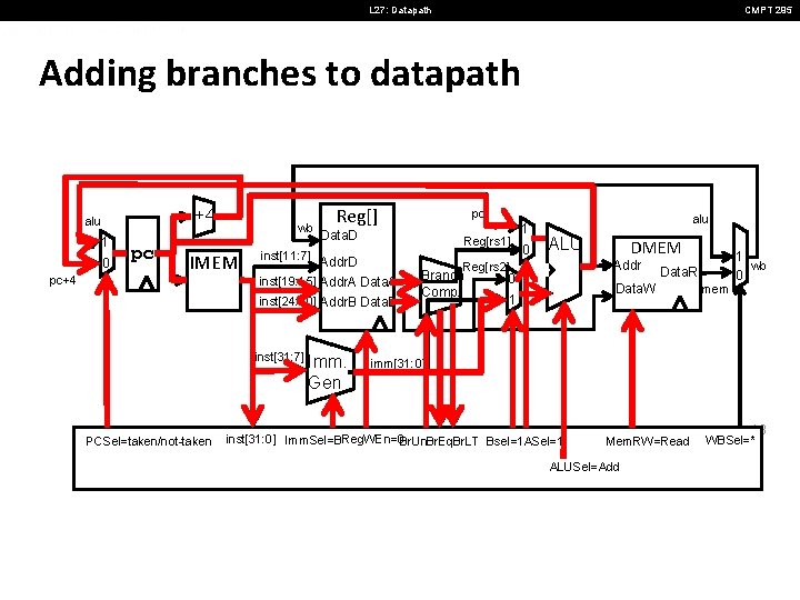
L 27: Datapath CMPT 295 Adding branches to datapath +4 alu 1 0 pc+4 pc wb IMEM Reg[] Data. D Reg[rs 1] inst[11: 7] Addr. D inst[24: 20] Addr. B Data. B PCSel=taken/not-taken Imm. Gen 1 0 alu ALU Branch Comp. DMEM Addr Reg[rs 2] inst[19: 15] Addr. A Data. A inst[31: 7] pc 0 Data. R Data. W 1 mem 1 wb 0 imm[31: 0] inst[31: 0] Imm. Sel=BReg. WEn=0 Br. Un. Br. Eq. Br. LT Bsel=1 ASel=1 Mem. RW=Read ALUSel=Add 13 WBSel=*

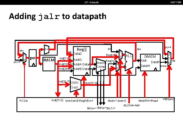
L 27: Datapath CMPT 295 Adding jalr to datapath +4 alu 1 pc+4 0 pc wb IMEM Reg[] pc Data. D Reg[rs 1] inst[11: 7] Addr. D inst[24: 20] Addr. B Data. B PCSel Imm. Gen 0 ALU DMEM Addr Reg[rs 2] inst[19: 15] Addr. A Data. A inst[31: 7] 1 Branch Comp. pc+4 alu 0 Data. R Data. W 1 mem 2 1 wb 0 imm[31: 0] inst[31: 0] Imm. Sel=B Reg. WEn=1 Bsel=1 Asel=0 Br. Un=* Br. Eq=* Br. LT=* Mem. RW=Read ALUSel=Add 14 WBSel=2

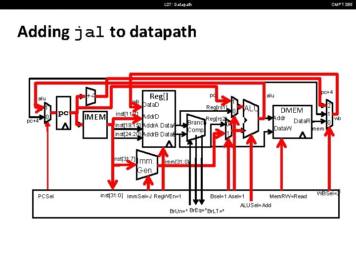
L 27: Datapath CMPT 295 Adding jal to datapath +4 alu 1 pc+4 0 pc wb IMEM Reg[] pc Data. D Reg[rs 1] inst[11: 7] Addr. D inst[24: 20] Addr. B Data. B PCSel Imm. Gen 0 ALU DMEM Addr Reg[rs 2] inst[19: 15] Addr. A Data. A inst[31: 7] 1 Branch Comp. pc+4 alu 0 Data. R Data. W 1 mem 2 1 wb 0 imm[31: 0] inst[31: 0] Imm. Sel=J Reg. WEn=1 Bsel=1 Asel=1 Br. Un=* Br. Eq=* Br. LT=* Mem. RW=Read ALUSel=Add 15 WBSel=2

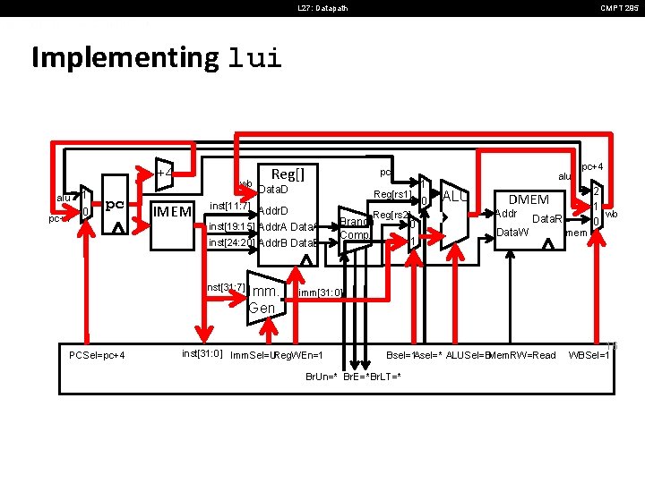
L 27: Datapath CMPT 295 Implementing lui +4 alu pc+4 1 0 pc wb IMEM Reg[] pc Data. D Reg[rs 1] inst[11: 7] Addr. D Reg[rs 2] inst[19: 15] Addr. A Data. A inst[24: 20] Addr. B Data. B inst[31: 7] PCSel=pc+4 Imm. Gen Branch Comp. 0 1 1 0 alu ALU pc+4 DMEM Addr Data. R Data. W mem 2 1 wb 0 imm[31: 0] inst[31: 0] Imm. Sel=UReg. WEn=1 Bsel=1 Asel=* ALUSel=BMem. RW=Read Br. Un=* Br. E=*Br. LT=* 16 WBSel=1

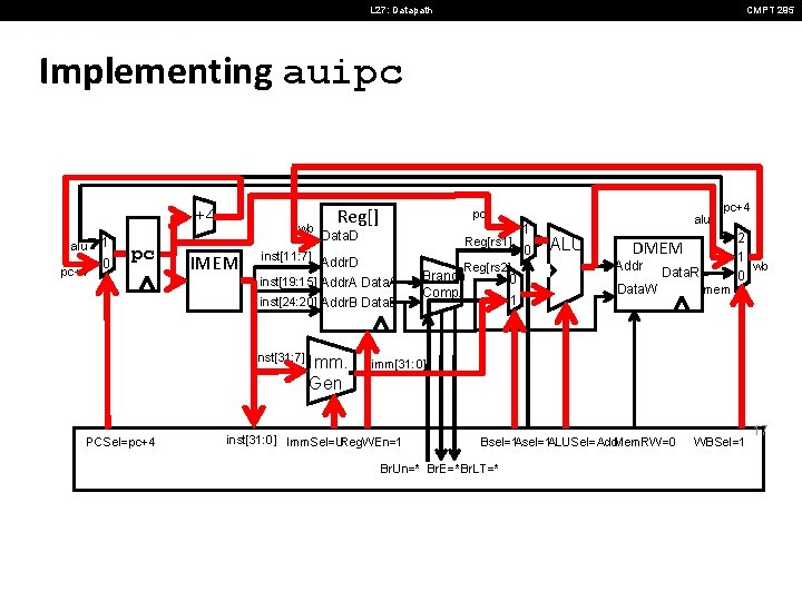
L 27: Datapath CMPT 295 Implementing auipc +4 alu pc+4 1 0 pc wb IMEM Reg[] pc Data. D Reg[rs 1] inst[11: 7] Addr. D Reg[rs 2] inst[19: 15] Addr. A Data. A inst[24: 20] Addr. B Data. B inst[31: 7] PCSel=pc+4 Imm. Gen Branch Comp. 0 1 1 0 alu ALU pc+4 DMEM Addr Data. R Data. W mem 2 1 wb 0 imm[31: 0] inst[31: 0] Imm. Sel=UReg. WEn=1 Bsel=1 ALUSel=Add. Mem. RW=0 Br. Un=* Br. E=*Br. LT=* WBSel=1 17