Knowledge Institute of Technology Department of Mechanical Engineering
- Slides: 25

Knowledge Institute of Technology Department of Mechanical Engineering PH 8151 - Engineering Physics (R 2017) Prepared by, B. Indumathi AP/Physics 1

CRYSTAL DEFECTS AND IMPERFECTIONS An ideal crystal is a perfect crystal in which each atom has identical surroundings. Real crystals are not perfect. A real crystal always has a large number of imperfections in the lattice. One can reduce crystal defects considerably, but can never eliminate them entirely. 2

CRYSTAL DEFECTS AND IMPERFECTIONS The study of imperfections has a two fold purpose, namely, A better understanding of crystals and how they affect the properties of metals. Exploration of possibilities of minimizing or eliminating these defects. The term “defect” or “imperfection” is generally used to describe any deviation from the perfect periodic array of atoms in the crystal. 3

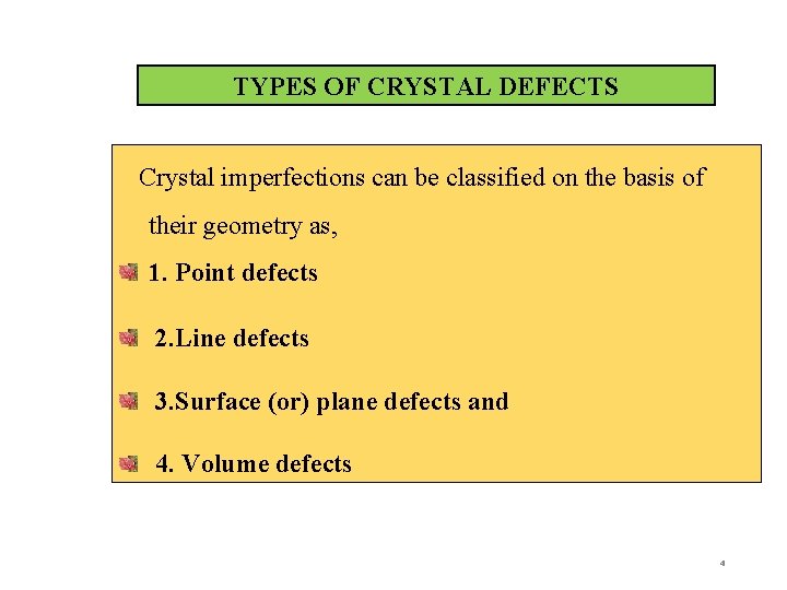
TYPES OF CRYSTAL DEFECTS Crystal imperfections can be classified on the basis of their geometry as, 1. Point defects 2. Line defects 3. Surface (or) plane defects and 4. Volume defects 4

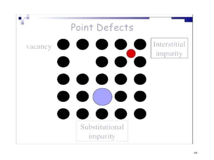
1. POINT DEFECTS They are imperfect point- like regions, one or two atomic diameters in size and hence referred to as ‘zero dimensional imperfections’. It takes place due to imperfect packing of atoms during crystallization. There are different kinds of point imperfections. a) Vacancies b) Impurities c) Interstitials 5

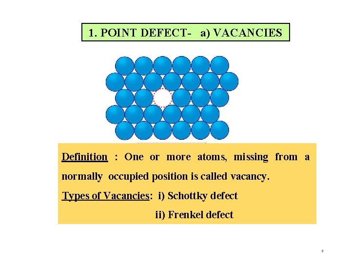
1. POINT DEFECT- a) VACANCIES Definition : One or more atoms, missing from a normally occupied position is called vacancy. Types of Vacancies: i) Schottky defect ii) Frenkel defect 6

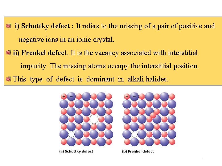
i) Schottky defect : It refers to the missing of a pair of positive and negative ions in an ionic crystal. ii) Frenkel defect: It is the vacancy associated with interstitial impurity. The missing atoms occupy the interstitial position. This type of defect is dominant in alkali halides. 7

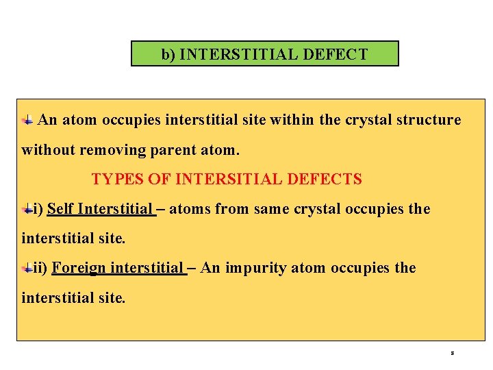
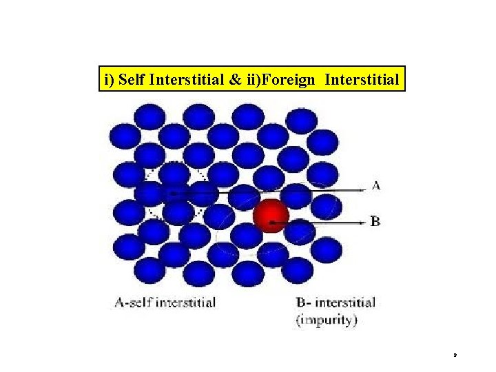
b) INTERSTITIAL DEFECT An atom occupies interstitial site within the crystal structure without removing parent atom. TYPES OF INTERSITIAL DEFECTS i) Self Interstitial – atoms from same crystal occupies the interstitial site. ii) Foreign interstitial – An impurity atom occupies the interstitial site. 8

i) Self Interstitial & ii)Foreign Interstitial 9

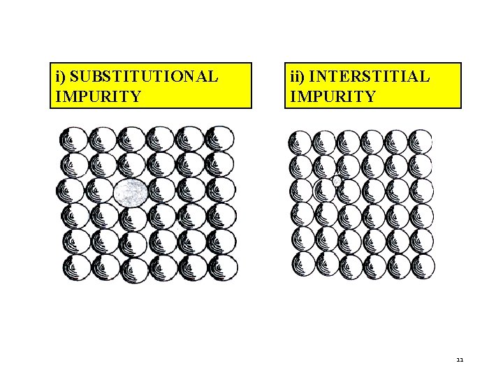
c) IMPURITIES When foreign atoms are added to crystal lattices, they are known as impurities. Types of Impurities i) Substitutional Impurity – Foreign atom replaces parent atom. Eg. , Doping of atoms in pure semiconductors. ii) Interstitial Impurity – A small size atom occupy interstitial space in parent crystal. Eg. , In FCC iron Carbon is added. 10

i) SUBSTITUTIONAL IMPURITY ii) INTERSTITIAL IMPURITY 11

12

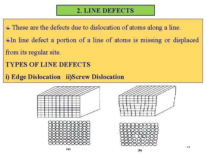
2. LINE DEFECTS These are the defects due to dislocation of atoms along a line. In line defect a portion of a line of atoms is missing or displaced from its regular site. TYPES OF LINE DEFECTS i) Edge Dislocation ii)Screw Dislocation 13

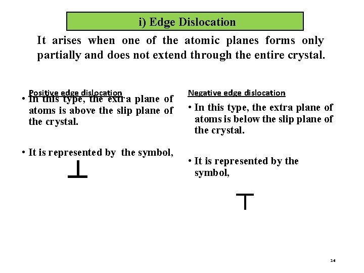
i) Edge Dislocation It arises when one of the atomic planes forms only partially and does not extend through the entire crystal. Positive edge dislocation • In this type, the extra plane of atoms is above the slip plane of the crystal. • It is represented by the symbol, ┴ Negative edge dislocation • In this type, the extra plane of atoms is below the slip plane of the crystal. • It is represented by the symbol, ┬ 14

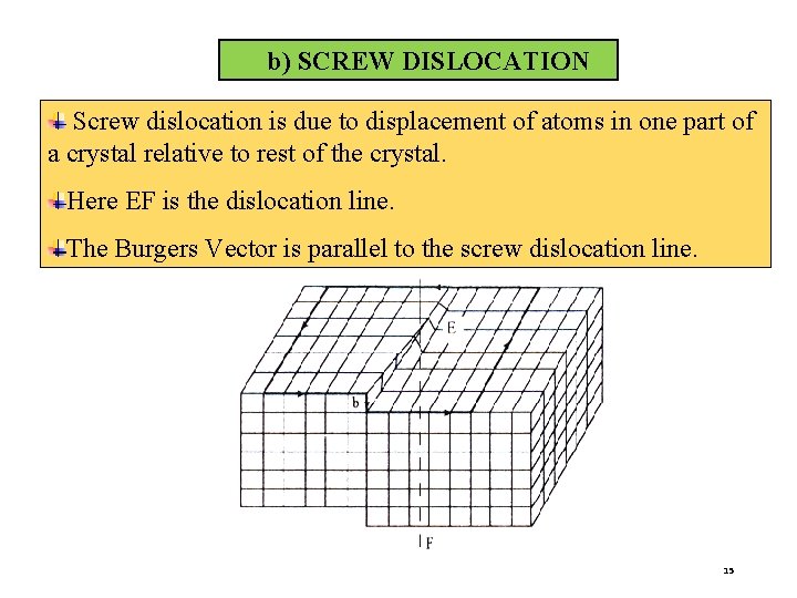
b) SCREW DISLOCATION Screw dislocation is due to displacement of atoms in one part of a crystal relative to rest of the crystal. Here EF is the dislocation line. The Burgers Vector is parallel to the screw dislocation line. 15

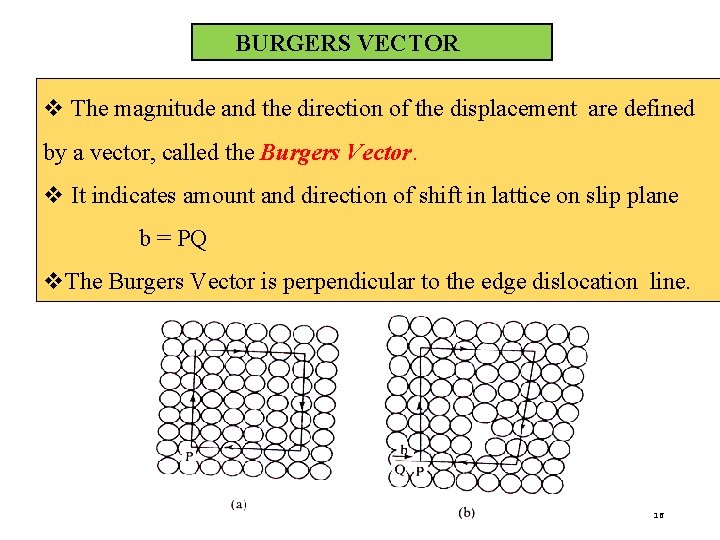
BURGERS VECTOR v The magnitude and the direction of the displacement are defined by a vector, called the Burgers Vector. v It indicates amount and direction of shift in lattice on slip plane b = PQ v. The Burgers Vector is perpendicular to the edge dislocation line. 16

3. SURFACE DEFECTS These are 2 dimensional defects. This type of defects are present on the surface of the material. TYPES OF SURFACE DEFECTS i) Grain boundaries ii) Tilt boundaries iii) Twin boundaries iv) Stacking Fault 17

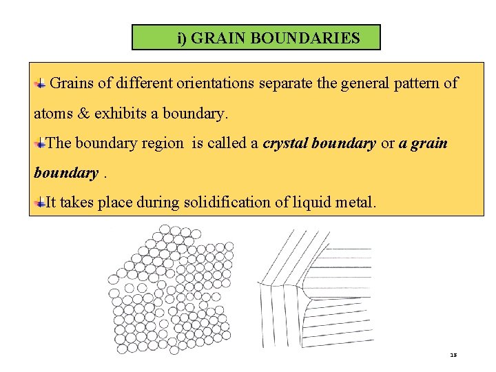
i) GRAIN BOUNDARIES Grains of different orientations separate the general pattern of atoms & exhibits a boundary. The boundary region is called a crystal boundary or a grain boundary. It takes place during solidification of liquid metal. 18

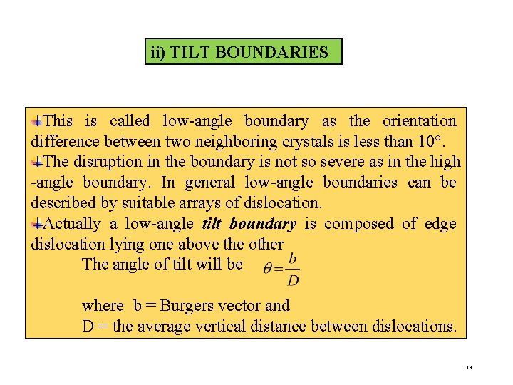
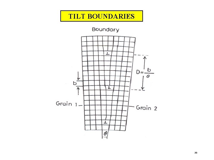
ii) TILT BOUNDARIES This is called low-angle boundary as the orientation difference between two neighboring crystals is less than 10°. The disruption in the boundary is not so severe as in the high -angle boundary. In general low-angle boundaries can be described by suitable arrays of dislocation. Actually a low-angle tilt boundary is composed of edge dislocation lying one above the other The angle of tilt will be where b = Burgers vector and D = the average vertical distance between dislocations. 19

TILT BOUNDARIES 20

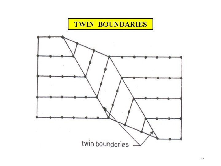
iii)TWIN BOUNDARIES If the atomic arrangement on one side of a boundary is a mirror reflection of the arrangement on the other side, then it is called as twin boundary. As they occur in pair, they are called twin boundaries. At one boundary, orientation of atomic arrangement changes. At another boundary, it is restored back. The region between the pair of boundaries is called the twinned region. These boundaries are easily identified under an optical microscope. 21

TWIN BOUNDARIES 22

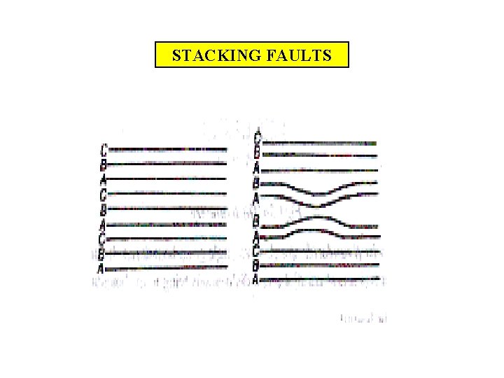
iv) STACKING FAULTS Whenever the stacking of atomic planes is not in a proper sequence throughout the crystal, the fault caused is known as stacking fault. For example, the stacking sequence in an ideal FCC crystal may be described as A-B-C-……. But the stacking fault may change the sequence to A-B-C-A-B-AB-C. The region in which the stacking fault occurs (A-B-A-B) forms a thin region and it becomes HCP. This thin region is a surface imperfection and is called a stacking fault. 23

STACKING FAULTS 24

4. VOLUME IMPERFECTIONS Volume defects such as cracks may arise in crystals when there is only small electrostatic dissimilarity between the stacking sequences of close packed planes in metals. Presence of a large vacancy or void space, when cluster of atoms are missed is also considered as a volume imperfection. Foreign particle inclusions and non crystalline regions which have the dimensions of the order of 0. 20 nm are also called as volume imperfections. 25