KNOWLEDGE INSTITUTE OF TECHNOLOGY DEPARTMENT OF ECE MICROPROCESSOR


- Slides: 26

KNOWLEDGE INSTITUTE OF TECHNOLOGY DEPARTMENT OF ECE MICROPROCESSOR AND MICROCONTROLLER Prepared by Mrs. A. Lelinadevi M. E Assistant processor/ECE

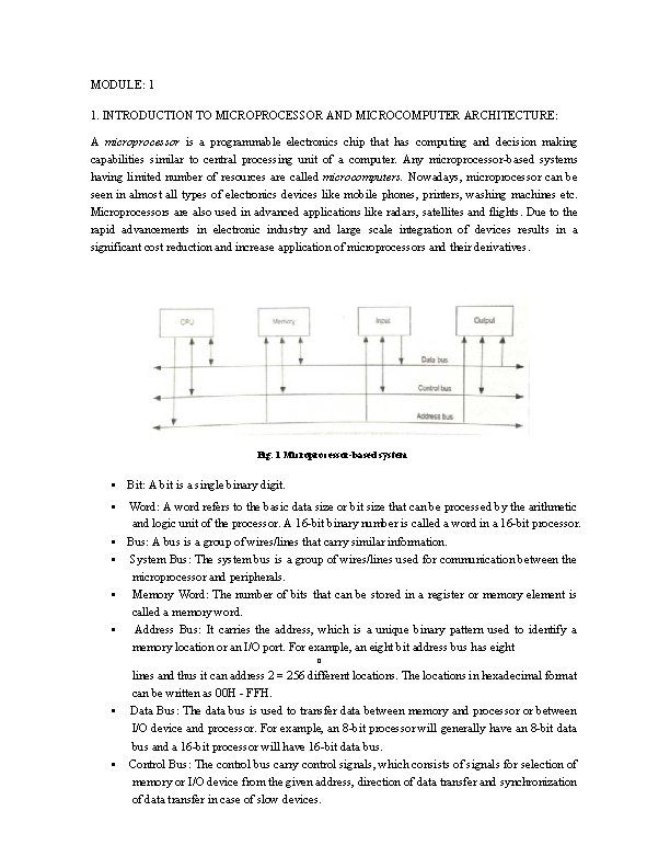
MODULE: 1 1. INTRODUCTION TO MICROPROCESSOR AND MICROCOMPUTER ARCHITECTURE: A microprocessor is a programmable electronics chip that has computing and decision making capabilities similar to central processing unit of a computer. Any microprocessor-based systems having limited number of resources are called microcomputers. Nowadays, microprocessor can be seen in almost all types of electronics devices like mobile phones, printers, washing machines etc. Microprocessors are also used in advanced applications like radars, satellites and flights. Due to the rapid advancements in electronic industry and large scale integration of devices results in a significant cost reduction and increase application of microprocessors and their derivatives. Fig. 1 Microprocessor-based system • Bit: A bit is a single binary digit. • Word: A word refers to the basic data size or bit size that can be processed by the arithmetic and logic unit of the processor. A 16 -bit binary number is called a word in a 16 -bit processor. Bus: A bus is a group of wires/lines that carry similar information. System Bus: The system bus is a group of wires/lines used for communication between the microprocessor and peripherals. Memory Word: The number of bits that can be stored in a register or memory element is called a memory word. Address Bus: It carries the address, which is a unique binary pattern used to identify a memory location or an I/O port. For example, an eight bit address bus has eight • • o • • lines and thus it can address 2 = 256 different locations. The locations in hexadecimal format can be written as 00 H - FFH. Data Bus: The data bus is used to transfer data between memory and processor or between I/O device and processor. For example, an 8 -bit processor will generally have an 8 -bit data bus and a 16 -bit processor will have 16 -bit data bus. Control Bus: The control bus carry control signals, which consists of signals for selection of memory or I/O device from the given address, direction of data transfer and synchronization of data transfer in case of slow devices.

A typical microprocessor consists of arithmetic and logic unit (ALU) in association with control unit to process the instruction execution. Almost all the microprocessors are based on the principle of store-program concept. In store-program concept, programs or instructions are sequentially stored in the memory locations that are to be executed. To do any task using a microprocessor, it is to be programmed by the user. So the programmer must have idea about its internal resources, features and supported instructions. Each microprocessor has a set of instructions, a list which is provided by the microprocessor manufacturer. The instruction set of a microprocessor is provided in two forms: binary machine code and mnemonics. Microprocessor communicates and operates in binary numbers 0 and 1. The set of instructions in the form of binary patterns is called a machine language and it is difficult for us to understand. Therefore, the binary patterns are given abbreviated names, called mnemonics, which forms the assembly language. The conversion of assembly-level language into binary machine-level language is done by using an application called assembler. Technology Used: The semiconductor manufacturing technologies used for chips are: • • Transistor-Transistor Logic (TTL) Emitter Coupled Logic (ECL) • Complementary Metal-Oxide Semiconductor (CMOS) Classification of Microprocessors: Based on their specification, application and architecture microprocessors are classified. Based on size of data bus: • • 4 -bit microprocessor 8 -bit microprocessor 16 -bit microprocessor 32 -bit microprocessor Based on application: • • • General-purpose microprocessor- used in general computer system and can be used by programmer for any application. Examples, 8085 to Intel Pentium. Microcontroller- microprocessor with built-in memory and ports and can be programmed for any generic control application. Example, 8051. Special-purpose processors- designed to handle special functions required for an application. Examples, digital signal processors and application-specific integrated circuit (ASIC) chips.

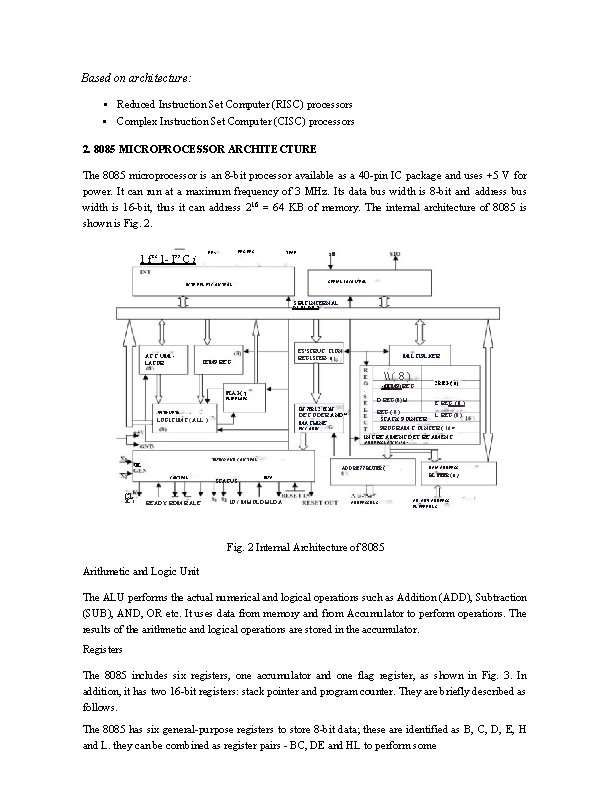
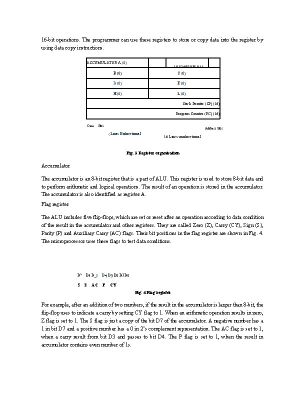
Based on architecture: • Reduced Instruction Set Computer (RISC) processors • Complex Instruction Set Computer (CISC) processors 2. 8085 MICROPROCESSOR ARCHITECTURE The 8085 microprocessor is an 8 -bit processor available as a 40 -pin IC package and uses +5 V for power. It can run at a maximum frequency of 3 MHz. Its data bus width is 8 -bit and address bus width is 16 -bit, thus it can address 216 = 64 KB of memory. The internal architecture of 8085 is shown is Fig. 2. RFs 1 f“ 1 - I” C i RFS TRAP Sill SERIAL I OCO. MROL IN TE RRL PT C ON TROL S BIT INTERNAL DATA BT S AC C UMl LATOR ES'STRUC TION REGISTER- o j TEMP REG Ml LTIPLXER \ ( 8 ) e. TEMP. RE C-. s I REG. C REG (' 8 ) FLAG ( ? ) FLIP FLOPS D REG(8) H IN STRl C TION RITIir. MFTI( DEC ODER AND* MACHINE LOGIC IMT ( ALL ) EN C ODIN E REG ( 8 ) L REG (8 ) STACK POINTER PROGRAM C Ol NTER ( 16 > INC RE AMENT DEC RE AMENT ADDRESS LATCH ( 16 > TIMING AND C ON TROL UK ADDRESS BLUER ( CONTROL CL OL 1 READY RDM R ALE STATUS IO / M HOLD HLDA DAIA ADDRESS BL FEER ( 8 } DMA ADDRESS BL S AD- ADfi. ADDRESS EL FFER BL S Fig. 2 Internal Architecture of 8085 Arithmetic and Logic Unit The ALU performs the actual numerical and logical operations such as Addition (ADD), Subtraction (SUB), AND, OR etc. It uses data from memory and from Accumulator to perform operations. The results of the arithmetic and logical operations are stored in the accumulator. Registers The 8085 includes six registers, one accumulator and one flag register, as shown in Fig. 3. In addition, it has two 16 -bit registers: stack pointer and program counter. They are briefly described as follows. The 8085 has six general-purpose registers to store 8 -bit data; these are identified as B, C, D, E, H and L. they can be combined as register pairs - BC, DE and HL to perform some

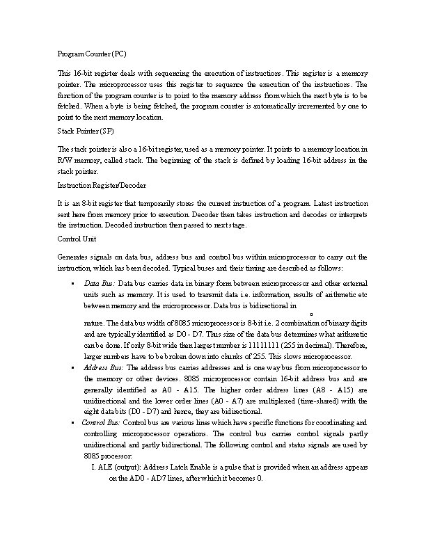
16 -bit operations. The programmer can use these registers to store or copy data into the register by using data copy instructions. ACCUMULATOR A (8) 1 1 FT Ad RFfr. TSTFR 1 1 B (8) C (8) D (8) E (8) H (8) L (8) Stack Pointer (SP) (16) Program Counter (PC) (16) Data Bus Address Bus ; Lines Bidirectional 16 Lines unidirectional Fig. 3 Register organisation Accumulator The accumulator is an 8 -bit register that is a part of ALU. This register is used to store 8 -bit data and to perform arithmetic and logical operations. The result of an operation is stored in the accumulator. The accumulator is also identified as register A. Flag register The ALU includes five flip-flops, which are set or reset after an operation according to data condition of the result in the accumulator and other registers. They are called Zero (Z), Carry (CY), Sign (S), Parity (P) and Auxiliary Carry (AC) flags. Their bit positions in the flag register are shown in Fig. 4. The microprocessor uses these flags to test data conditions. D? De D_s D 4 D 3 D 2 DI Do S Z AC P CY Fig. 4 Flag register For example, after an addition of two numbers, if the result in the accumulator is larger than 8 -bit, the flip-flop uses to indicate a carry by setting CY flag to 1. When an arithmetic operation results in zero, Z flag is set to 1. The S flag is just a copy of the bit D 7 of the accumulator. A negative number has a 1 in bit D 7 and a positive number has a 0 in 2’s complement representation. The AC flag is set to 1, when a carry result from bit D 3 and passes to bit D 4. The P flag is set to 1, when the result in accumulator contains even number of 1 s.

Program Counter (PC) This 16 -bit register deals with sequencing the execution of instructions. This register is a memory pointer. The microprocessor uses this register to sequence the execution of the instructions. The function of the program counter is to point to the memory address from which the next byte is to be fetched. When a byte is being fetched, the program counter is automatically incremented by one to point to the next memory location. Stack Pointer (SP) The stack pointer is also a 16 -bit register, used as a memory pointer. It points to a memory location in R/W memory, called stack. The beginning of the stack is defined by loading 16 -bit address in the stack pointer. Instruction Register/Decoder It is an 8 -bit register that temporarily stores the current instruction of a program. Latest instruction sent here from memory prior to execution. Decoder then takes instruction and decodes or interprets the instruction. Decoded instruction then passed to next stage. Control Unit Generates signals on data bus, address bus and control bus within microprocessor to carry out the instruction, which has been decoded. Typical buses and their timing are described as follows: • Data Bus: Data bus carries data in binary form between microprocessor and other external units such as memory. It is used to transmit data i. e. information, results of arithmetic etc between memory and the microprocessor. Data bus is bidirectional in o nature. The data bus width of 8085 microprocessor is 8 -bit i. e. 2 combination of binary digits and are typically identified as D 0 - D 7. Thus size of the data bus determines what arithmetic can be done. If only 8 -bit wide then largest number is 1111 (255 in decimal). Therefore, larger numbers have to be broken down into chunks of 255. This slows microprocessor. • Address Bus: The address bus carries addresses and is one way bus from microprocessor to the memory or other devices. 8085 microprocessor contain 16 -bit address bus and are generally identified as A 0 - A 15. The higher order address lines (A 8 - A 15) are unidirectional and the lower order lines (A 0 - A 7) are multiplexed (time-shared) with the eight data bits (D 0 - D 7) and hence, they are bidirectional. • Control Bus: Control bus are various lines which have specific functions for coordinating and controlling microprocessor operations. The control bus carries control signals partly unidirectional and partly bidirectional. The following control and status signals are used by 8085 processor: I. ALE (output): Address Latch Enable is a pulse that is provided when an address appears on the AD 0 - AD 7 lines, after which it becomes 0.

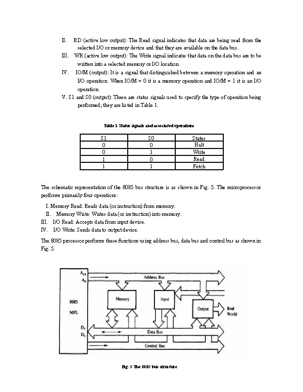
II. RD (active low output): The Read signal indicates that data are being read from the selected I/O or memory device and that they are available on the data bus. III. WR (active low output): The Write signal indicates that data on the data bus are to be written into a selected memory or I/O location. IV. IO/M (output): It is a signal that distinguished between a memory operation and an I/O operation. When IO/M = 0 it is a memory operation and IO/M = 1 it is an I/O operation. V. S 1 and S 0 (output): These are status signals used to specify the type of operation being performed; they are listed in Table 1 Status signals and associated operations S 1 0 0 1 1 S 0 0 1 States Halt Write Read Fetch The schematic representation of the 8085 bus structure is as shown in Fig. 5. The microprocessor performs primarily four operations: I. Memory Read: Reads data (or instruction) from memory. II. Memory Write: Writes data (or instruction) into memory. III. I/O Read: Accepts data from input device. IV. I/O Write: Sends data to output device. The 8085 processor performs these functions using address bus, data bus and control bus as shown in Fig. 5 The 8085 bus structure

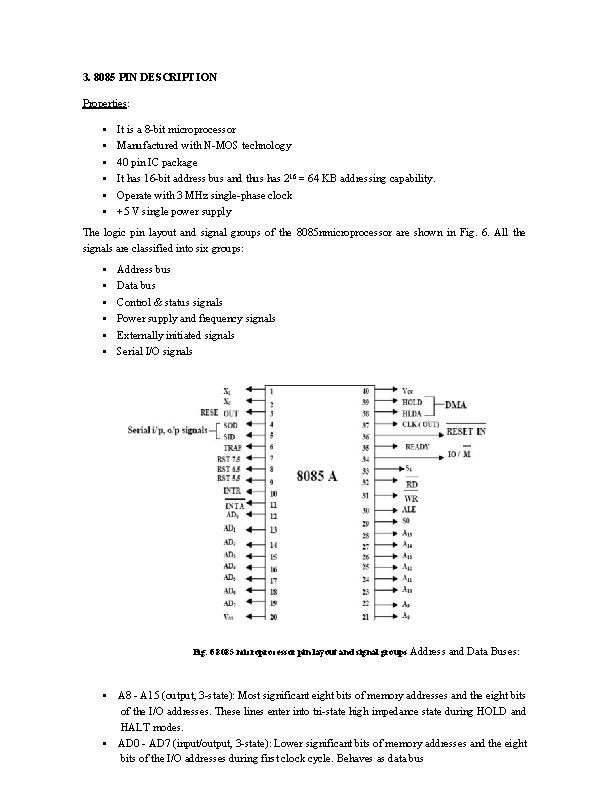
3. 8085 PIN DESCRIPTION Properties: • • It is a 8 -bit microprocessor Manufactured with N-MOS technology • • 40 pin IC package It has 16 -bit address bus and thus has 216 = 64 KB addressing capability. Operate with 3 MHz single-phase clock +5 V single power supply The logic pin layout and signal groups of the 8085 nmicroprocessor are shown in Fig. 6. All the signals are classified into six groups: • • • Address bus Data bus Control & status signals Power supply and frequency signals Externally initiated signals • Serial I/O signals Fig. 6 8085 microprocessor pin layout and signal groups Address • • and Data Buses: A 8 - A 15 (output, 3 -state): Most significant eight bits of memory addresses and the eight bits of the I/O addresses. These lines enter into tri-state high impedance state during HOLD and HALT modes. AD 0 - AD 7 (input/output, 3 -state): Lower significant bits of memory addresses and the eight bits of the I/O addresses during first clock cycle. Behaves as data bus

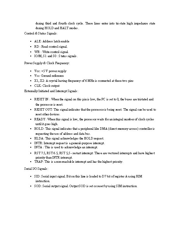
during third and fourth clock cycle. These lines enter into tri-state high impedance state during HOLD and HALT modes. Control & Status Signals: • ALE: Address latch enable • RD : Read control signal. • • WR : Write control signal. IO/M, S 1 and S 0 : Status signals. Power Supply & Clock Frequency: • Vcc: +5 V power supply • Vss: Ground reference • X 1, X 2: A crystal having frequency of 6 MHz is connected at these two pins • CLK: Clock output Externally Initiated and Interrupt Signals: • RESET IN : When the signal on this pin is low, the PC is set to 0, the buses are tristated and the processor is reset. • • RESET OUT: This signal indicates that the processor is being reset. The signal can be used to reset other devices. READY: When this signal is low, the processor waits for an integral number of clock cycles until it goes high. HOLD: This signal indicates that a peripheral like DMA (direct memory access) controller is requesting the use of address and data bus. HLDA: This signal acknowledges the HOLD request. INTR: Interrupt request is a general-purpose interrupt. INTA : This is used to acknowledge an interrupt. RST 7. 5, RST 6. 5, RST 5, 5 - restart interrupt: These are vectored interrupts and have highest priority than INTR interrupt. TRAP: This is a non-maskable interrupt and has the highest priority. Serial I/O Signals: • • SID: Serial input signal. Bit on this line is loaded to D 7 bit of register A using RIM instruction. SOD: Serial output signal. Output SOD is set or reset by using SIM instruction.

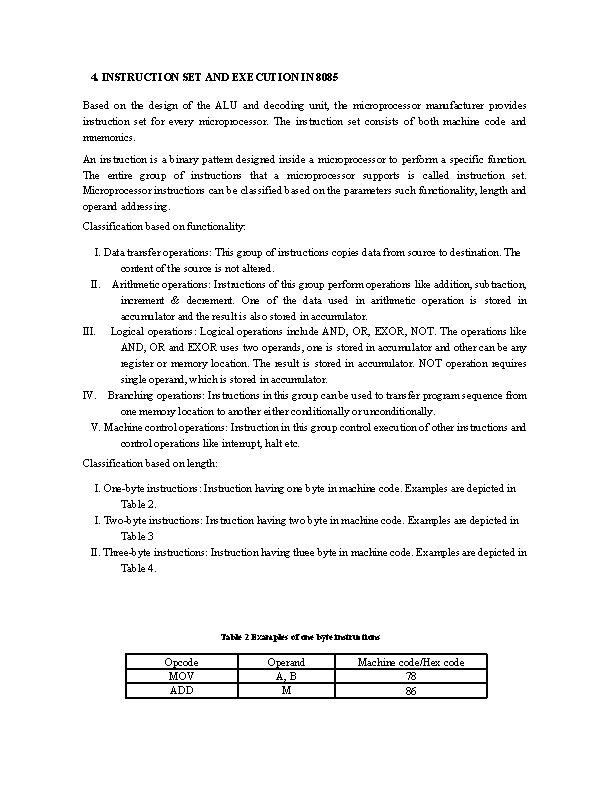
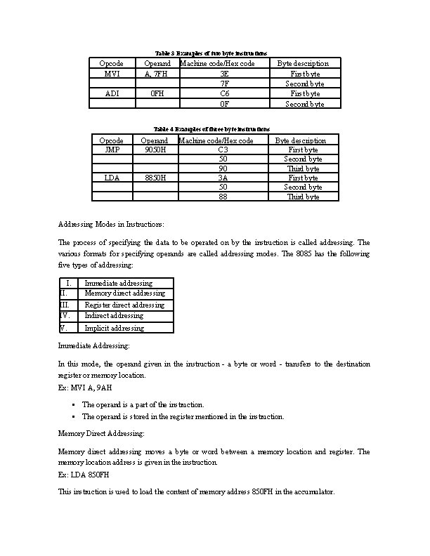
4. INSTRUCTION SET AND EXECUTION IN 8085 Based on the design of the ALU and decoding unit, the microprocessor manufacturer provides instruction set for every microprocessor. The instruction set consists of both machine code and mnemonics. An instruction is a binary pattern designed inside a microprocessor to perform a specific function. The entire group of instructions that a microprocessor supports is called instruction set. Microprocessor instructions can be classified based on the parameters such functionality, length and operand addressing. Classification based on functionality: I. Data transfer operations: This group of instructions copies data from source to destination. The content of the source is not altered. II. Arithmetic operations: Instructions of this group perform operations like addition, subtraction, increment & decrement. One of the data used in arithmetic operation is stored in accumulator and the result is also stored in accumulator. III. Logical operations: Logical operations include AND, OR, EXOR, NOT. The operations like AND, OR and EXOR uses two operands, one is stored in accumulator and other can be any register or memory location. The result is stored in accumulator. NOT operation requires single operand, which is stored in accumulator. IV. Branching operations: Instructions in this group can be used to transfer program sequence from one memory location to another either conditionally or unconditionally. V. Machine control operations: Instruction in this group control execution of other instructions and control operations like interrupt, halt etc. Classification based on length: I. One-byte instructions: Instruction having one byte in machine code. Examples are depicted in Table 2. I. Two-byte instructions: Instruction having two byte in machine code. Examples are depicted in Table 3 II. Three-byte instructions: Instruction having three byte in machine code. Examples are depicted in Table 4. Table 2 Examples of one byte instructions Opcode MOV ADD Operand A, B M Machine code/Hex code 78 86

Table 3 Examples of two byte instructions Opcode MVI Operand A, 7 FH ADI 0 FH Machine code/Hex code 3 E 7 F C 6 0 F Byte description First byte Second byte Table 4 Examples of three byte instructions Opcode JMP Operand 9050 H LDA 8850 H Machine code/Hex code C 3 50 90 3 A 50 88 Byte description First byte Second byte Third byte Addressing Modes in Instructions: The process of specifying the data to be operated on by the instruction is called addressing. The various formats for specifying operands are called addressing modes. The 8085 has the following five types of addressing: I. III. IV. Immediate addressing Memory direct addressing Register direct addressing Indirect addressing V. Implicit addressing Immediate Addressing: In this mode, the operand given in the instruction - a byte or word - transfers to the destination register or memory location. Ex: MVI A, 9 AH • The operand is a part of the instruction. • The operand is stored in the register mentioned in the instruction. Memory Direct Addressing: Memory direct addressing moves a byte or word between a memory location and register. The memory location address is given in the instruction. Ex: LDA 850 FH This instruction is used to load the content of memory address 850 FH in the accumulator.

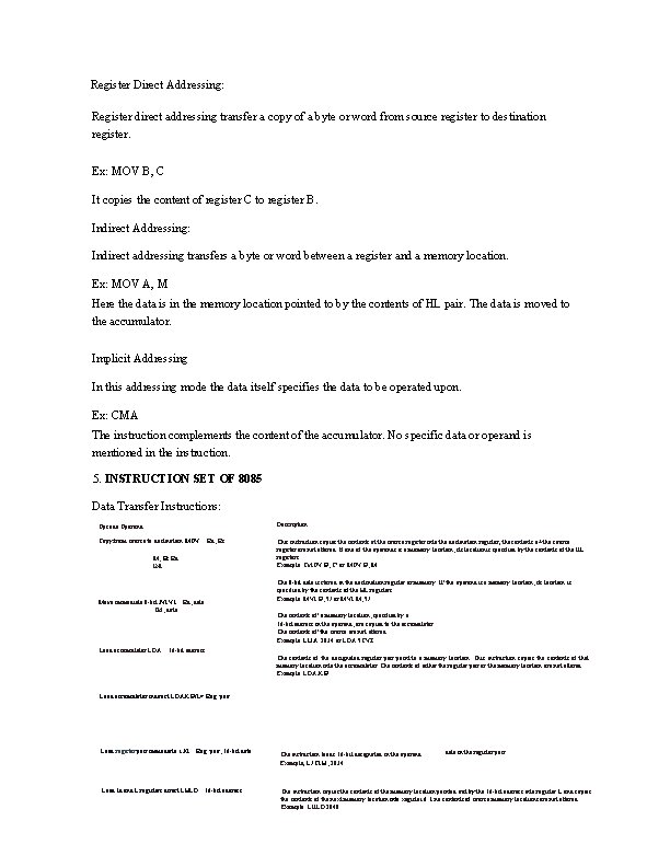
Register Direct Addressing: Register direct addressing transfer a copy of a byte or word from source register to destination register. Ex: MOV B, C It copies the content of register C to register B. Indirect Addressing: Indirect addressing transfers a byte or word between a register and a memory location. Ex: MOV A, M Here the data is in the memory location pointed to by the contents of HL pair. The data is moved to the accumulator. Implicit Addressing In this addressing mode the data itself specifies the data to be operated upon. Ex: CMA The instruction complements the content of the accumulator. No specific data or operand is mentioned in the instruction. 5. INSTRUCTION SET OF 8085 Data Transfer Instructions: Description Opcode Operand Copy from source to destination MOV Rd, Rs M, Rs Rd. INI The 8 -bit data is stored in the destination register or memory. II' the operand is a memory location, its location is specified by the contents of the HL registers. Example: MVI B, 57 or MVI M, 57 Move immediate 8 -bit JVl VI Rd, data Tvf, data Load accumulator LDA This instruction copies the contents ot the source register into the destination register; the contents o± the source register are not altered. If one of the operands is a memory location, its location is specified by the contents of the IIL registers. Example: Tvl. OV B, C 1 or MOV B, M The contents of' a memory location, specified by a 16 -bit address in the operand, are copied to the accumulator. The contents of' the source are not altered. Example: LI 3 A. 2034 or LDA 5 CVZ 16 -bit address The contents of the designated register pair point to a memory location. This instruction copies the contents of that memory location into the accumulator. The contents of either the register pair or the memory location are not altered. Example: LDAX B Load accumulator indirect LDAX B/L> Reg. pair Load register pair immediate 1 XI Reg. pair, 16 -bit data Load Id and L registers direct LHLD 16 -bit address The instruction loads 16 -bil designated in the operand. Example; L 7 CI H, 2034 data in the register pair The instruction copies the contents of the memory location pointed out by the 16 -bit address into register L and copies the contents of the next memory location into xegistei if. I ne contents of source memory locations are not altered. Example: LIILD 2040

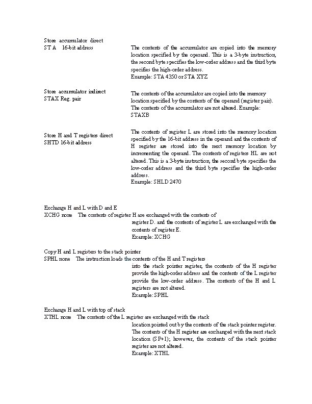
Store accumulator direct ST A 16 -bit address Store accumulator indirect STAX Reg. pair Store H and T registers direct SHTD 16 -bit address The contents of the accumulator are copied into the memory location specified by the operand. This is a 3 -byte instruction, the second byte specifies the low-order address and the third byte specifies the high-order address. Example: STA 4350 or STA XYZ The contents of the accumulator are copied into the memory location specified by the contents of the operand (register pair). The contents of the accumulator are not altered. Example: STAXB The contents of register L are stored into the memory location specified by the 16 -bit address in the operand the contents of H register are stored into the next memory location by incrementing the operand. The contents of registers HL are not altered. This is a 3 -byte instruction, the second byte specifies the low-order address and the third byte specifies the high-order address. Example: SHLD 2470 Exchange H and L with D and E XCHG none The contents of register H are exchanged with the contents of register D. and the contents of register L are exchanged with the contents of register E. Example: XCHG Copy H and L registers to the stack pointer SPHL none The instruction loads the contents of the H and T registers into the stack pointer register, the contents of the H register provide the high-order address and the contents of the L register provide the low-order address. The contents of the H and L registers are not altered. Example: SPHL Exchange H and L with top of stack XTHL none The contents of the L register are exchanged with the stack location pointed out by the contents of the stack pointer register. The contents of the H register are exchanged with the next stack location (SP+1); however, the contents of the stack pointer register are not altered. Example: XTHL

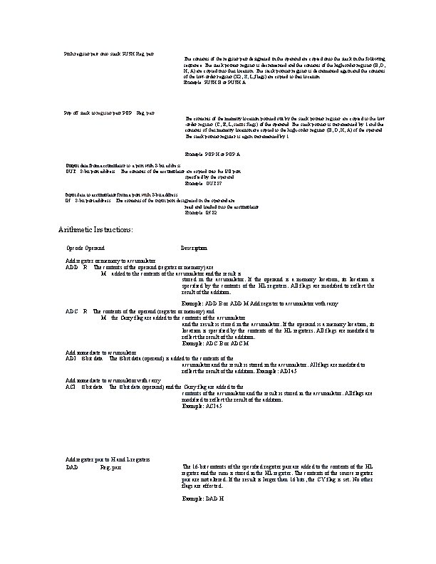
Push register pair onto stack PUSH Reg. pair The contents of the register pair designated in the operand are copied onto the stack in the following sequence. The stack pointer register is decremented and the contents of the high-order register (B, D, H, A) are copied into that location. The stack pointer register is decremented again and the contents of the low-order register (X 2, E, L, flags) are copied to that location. Example: PUSH B or PUSH A Pop off stack to register pair POP Reg. pair The contents of the memory location pointed out by the stack pointer register are copied to the low -order register (C, E, L, status flags) of the operand. The stack pointer is incremented by 1 and the contents of that memory location are copied to the high-order register (B, D, H, A) of the operand. The stack pointer register is again incremented by 1. Example: POP H or POP A Output data from accumulator to a port with 8 -bit address OUT 8 -bit port address The contents of the accumulator are copied into the I/O port specified by the operand. Example: OUT 87 Input data to accumulator from a port with 8 -bit address IN 8 -bit port address The contents of the input port designated in the operand are read and loaded into the accumulator. Example: IN 82 Arithmetic Instructions: Opcode Operand Description Add register or memory to accumulator ADD R The contents of the operand (register or memory) are M added to the contents of the accumulator and the result is stored in the accumulator. If the operand is a memory location, its location is specified by the contents of the HL registers. All flags are modified to reflect the result of the addition. ADC R Example: ADD B or ADD M Add register to accumulator with carry The contents of the operand (register or memory) and M the Carry flag are added to the contents of the accumulator and the result is stored in the accumulator. If the operand is a memory location, its location is specified by the contents of the HL registers. All flags are modified to reflect the result of the addition. Example: ADC B or ADC M Add immediate to accumulator ADI 8 -bit data The 8 -bit data (operand) is added to the contents of the accumulator and the result is stored in the accumulator. All flags are modified to reflect the result of the addition. Example: ADI 45 Add immediate to accumulator with carry ACI 8 -bit data The 8 -bit data (operand) and the Carry flag are added to the contents of the accumulator and the result is stored in the accumulator. All flags are modified to reflect the result of the addition. Example: ACI 45 Add register pair to H and L registers DAD Reg. pair The 16 -bit contents of the specified register pair are added to the contents of the HL register and the sum is stored in the HL register. The contents of the source register pair are not altered. If the result is larger than 16 bits, the CY flag is set. No other flags are affected. Example: DAD H

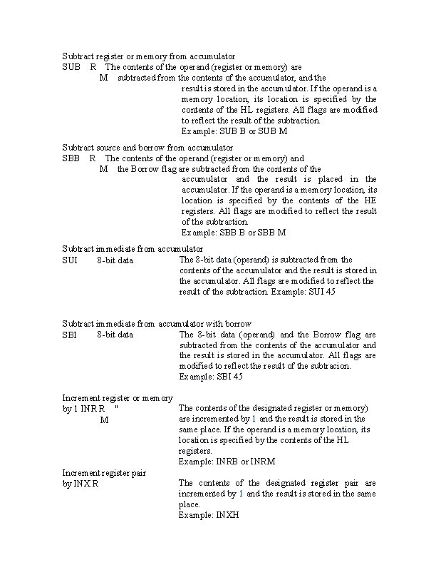
Subtract register or memory from accumulator SUB R The contents of the operand (register or memory) are M subtracted from the contents of the accumulator, and the result is stored in the accumulator. If the operand is a memory location, its location is specified by the contents of the HL registers. All flags are modified to reflect the result of the subtraction. Example: SUB B or SUB M Subtract source and borrow from accumulator SBB R The contents of the operand (register or memory) and M the Borrow flag are subtracted from the contents of the accumulator and the result is placed in the accumulator. If the operand is a memory location, its location is specified by the contents of the HE registers. All flags are modified to reflect the result of the subtraction. Example: SBB B or SBB M Subtract immediate from accumulator The 8 -bit data (operand) is subtracted from the 8 -bit data SUI contents of the accumulator and the result is stored in the accumulator. All flags are modified to reflect the result of the subtraction. Example: SUI 45 Subtract immediate from accumulator with borrow The 8 -bit data (operand) and the Borrow flag are 8 -bit data SBI subtracted from the contents of the accumulator and the result is stored in the accumulator. All flags are modified to reflect the result of the subtracion. Example: SBI 45 Increment register or memory The contents of the designated register or memory) by 1 INR R " are incremented by 1 and the result is stored in the M same place. If the operand is a memory location, its location is specified by the contents of the HL registers. Example: INRB or INRM Increment register pair The contents of the designated register pair are by INX R incremented by 1 and the result is stored in the same place. Example: INXH

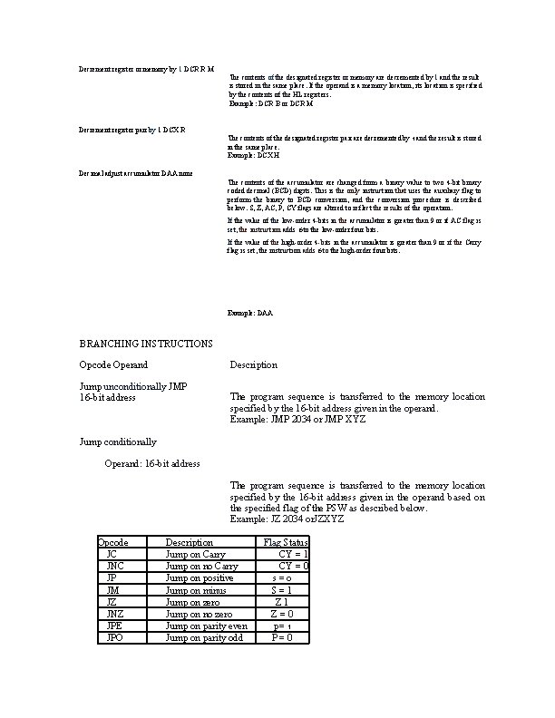
Decrement register or memory by 1 DCR R M Decrement register pair by 1 DCX R The contents of the designated register or memory are decremented by 1 and the result is stored in the same place. If the operand is a memory location, its location is specified by the contents of the HL registers. Example: DCR B or DCR M The contents of the designated register pair are decremented by 1 and the result is stored in the same place. Example: DCX H Decimal adjust accumulator DAA none The contents of the accumulator are changed from a binary value to two 4 -bit binary coded decimal (BCD) digits. This is the only instruction that uses the auxiliary flag to perform the binary to BCD conversion, and the conversion procedure is described below. S, Z, AC, P, CY flags are altered to reflect the results of the operation. If the value of the low-order 4 -bits in the accumulator is greater than 9 or if AC flag is set, the instruction adds 6 to the low-order four bits. If the value of the high-order 4 -bits in the accumulator is greater than 9 or if the Carry flag is set, the instruction adds 6 to the high-order four bits. Example: DAA BRANCHING INSTRUCTIONS Opcode Operand Description Jump unconditionally JMP 16 -bit address The program sequence is transferred to the memory location specified by the 16 -bit address given in the operand. Example: JMP 2034 or JMP XYZ Jump conditionally Operand: 16 -bit address The program sequence is transferred to the memory location specified by the 16 -bit address given in the operand based on the specified flag of the PSW as described below. Example: JZ 2034 or. JZXYZ Opcode JC JNC JP JM JZ JNZ JPE JPO Description Jump on Carry Jump on no Carry Jump on positive Jump on minus Jump on zero Jump on no zero Jump on parity even Jump on parity odd Flag Status CY = 1 CY = 0 s=o S=1 Z 1 Z=0 p= 1 P=0

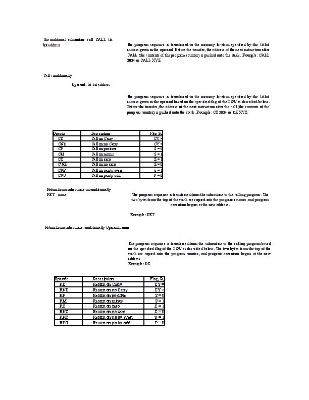
Unconditional subroutine call CALL 16 bit address The program sequence is transferred to the memory location specified by the 16 -bit address given in the operand. Before the transfer, the address of the next instruction after CALL (the contents of the program counter) is pushed onto the stack. Example: CALL 2034 or CALL XYZ Call conditionally Operand: 16 -bit address The program sequence is transferred to the memory location specified by the 16 -bit address given in the operand based on the specified flag of the PSW as described below. Before the transfer, the address of the next instruction after the call (the contents of the program counter) is pushed onto the stack. Example: CZ 2034 or CZ XYZ Opcode CC CNC CP CM CZ C'NZ CPE CPO Description Call on Carry Call on no Carry Call on positive Call on minus Call on zero Call on no zero Call on parity even Call on parity odd Flag St; CY = S=0 S=1 Z=0 p=1 P=0 Return from subroutine unconditionally RET none The program sequence is transferred from the subroutine to the calling program. The two bytes from the top of the stack are copied into the program counter, and program execution begins at the new address. Example: RET Return from subroutine conditionally Operand: none The program sequence is transferred from the subroutine to the calling program based on the specified flag of the PSW as described below. The two bytes from the top of the stack are copied into the program counter, and program execution begins at the new address. Example: RZ Opcode RC RNC RP RM RZ RNZ RPE RPO Description Return on Carry Return on no Carry Return on positive Return on minus Return on zero Return on no zero Return on parity even Return on parity odd Flag St; CY = S=0 S=1 Z=0 p=1 P=0

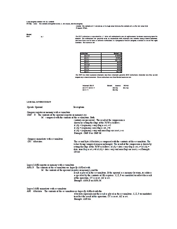
Load program counter with III. contents PCTHL none The contents of registers H and. L are copied, into the program counter. The contents of 11 are placed as the high-order byte and the contents of L as the low-order byte. Example: PCHL Restart RST 0 -7 The RST instruction is equivalent to a 1 -byte call instruction to one of eight memory locations depending upon the number. The instructions are generally used in conjunction with interrupts and inserted using external hardware. However these cair be used as software instructions in a program to transfer program execution to one of the eight locations. The addresses are: Instruction RST O RST 1 RST 2 RST 3 RST A RST 5 RST 6 RST 7 Restart Acl OOOOM OOOSH OO 1 OH 0018 H 0020 H 0028 H 0030 H 003 8 H The 8085 has four additional interrupts and these interrupts generate RST instructions internally and thus do not require any external hardware. These instructions and their Restart addresses are: Interrupt TRAP RST 5. 5 RST 6. 5 RST 7. 5 Restart Address 002 CH 003 CH 0024 H 003 -4 H LOGICAL INSTRUCTIONS Opcode Operand Description Compare register or memory with accumulator CMP R The contents of the operand (register or memory) are M compared with the contents of the accumulator. Both contents are preserved. The result of the comparison is shown by setting the flags of the PSW as follows: if (A) < (reg/mem): carry flag is set, s=l if (A) = (reg/mem): zero flag is set, s=0 if (A) > (reg/mem): carry and zero flags are reset, s=0 Example: CMP B or CMP M Compare immediate with accumulator CPI 8 -bit data The second byte (8 -bit data) is compared with the contents of the accumulator. The values being compared remain unchanged. The result of the comparison is shown by setting the flags of the PSW as follows: if (A) < data: carry flag is set, s=l if (A) = data: zero flag is set, s=0 if (A) > data: carry and zero flags are reset, s=0 Example: CPI 89 Logical AND register or memory with accumulator ANA R The contents of the accumulator are logically ANDed with M the contents of the operand (register or memory), and the result is placed in the accumulator. If the operand is a memory location, its address is specified by the contents of HL registers. S, Z, P are modified to reflect the result of the operation. CY is reset. AC is set. Example: ANA B or ANA M Logical AND immediate with accumulator ANI 8 -bit data The contents of the accumulator are logically ANDed with the 8 -bit data (operand) and the result is placed in the accumulator. S, Z, P are modified to reflect the result of the operation. CY is reset. AC is set. Example: ANI 86

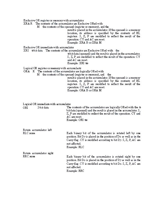
Exclusive OR register or memory with accumulator XRA R The contents of the accumulator are Exclusive ORed with M the contents of the operand (register or memory), and the result is placed in the accumulator. If the operand is a memory location, its address is specified by the contents of HL registers. S, Z, P are modified to reflect the result of the operation. CY and AC are reset. Example: XRA B or XRA M Exclusive OR immediate with accumulator XRI 8 -bit data The contents of the accumulator are Exclusive ORed with the 8 -bit data (operand) and the result is placed in the accumulator. S, Z, P are modified to reflect the result of the operation. CY and AC are reset. Example: XRI 86 Logical OR register or memory with accumulaotr ORA R The contents of the accumulator are logically ORed with M the contents of the operand (register or memory), and the result is placed in the accumulator. If the operand is a memory location, its address is specified by the contents of HL registers. S, Z, P are modified to reflect the result of the operation. CY and AC are reset. Example: ORA B or ORA M Logical OR immediate with accumulator The contents of the accumulator are logically ORed with the 85 -bit data ORI bit data (operand) and the result is placed in the accumulator. S, Z, P are modified to reflect the result of the operation. CY and AC are reset. Example: ORI 86 Rotate accumulator left RLC none Rotate accumulator right RRC none Each binary bit of the accumulator is rotated left by one position. Bit D 7 is placed in the position of Do as well as in the Carry flag. CY is modified according to bit D 7. S, Z, P, AC are not affected. Example: RLC Each binary bit of the accumulator is rotated right by one position. Bit Do is placed in the position of D 7 as well as in the Carry flag. CY is modified according to bit Do. S, Z, P, AC are not affected. Example: RRC

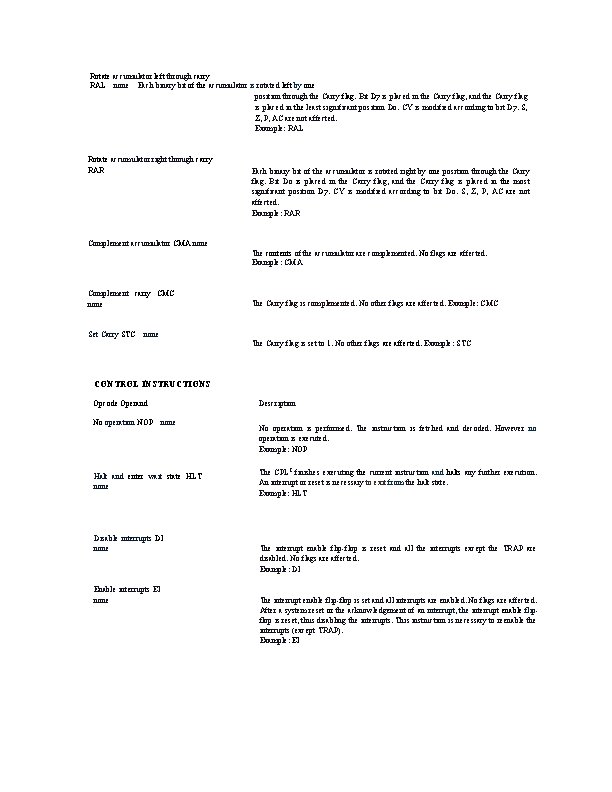
Rotate accumulator left through carry RAL none Each binary bit of the accumulator is rotated left by one position through the Carry flag. Bit D 7 is placed in the Carry flag, and the Carry flag is placed in the least significant position Do. CY is modified according to bit D 7. S, Z, P, AC are not affected. Example: RAL Rotate accumulator right through carry RAR Each binary bit of the accumulator is rotated right by one position through the Carry flag. Bit Do is placed in the Carry flag, and the Carry flag is placed in the most significant position D 7. CY is modified according to bit Do. S, Z, P, AC are not affected. Example: RAR Complement accumulator CMA none The contents of the accumulator are complemented. No flags are affected. Example: CMA Complement carry CMC none Set Carry STC The Carry flag is complemented. No other flags are affected. Example: CMC none The Carry flag is set to 1. No other flags are affected. Example: STC CONTROL INSTRUCTIONS Opcode Operand No operation NOP Description none Halt and enter wait state HLT none Disable interrupts DI none Enable interrupts El none No operation is performed. The instruction is fetched and decoded. However no operation is executed. Example: NOP The CPLT finishes executing the current instruction and halts any further execution. An interrupt or reset is necessary to exit from the halt state. Example: HLT The interrupt enable flip-flop is reset and all the interrupts except the TRAP are disabled. No flags are affected. Example: DI The interrupt enable flip-flop is set and all interrupts are enabled. No flags are affected. After a system reset or the acknowledgement of an interrupt, the interrupt enable flipflop is reset, thus disabling the interrupts. This instruction is necessary to reenable the interrupts (except TRAP). Example: El

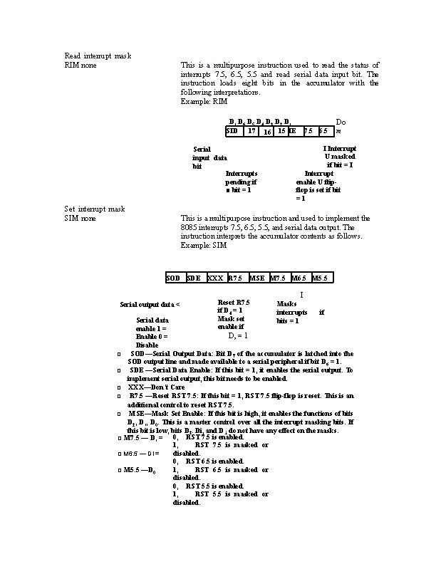
Read interrupt mask RIM none This is a multipurpose instruction used to read the status of interrupts 7. 5, 6. 5, 5. 5 and read serial data input bit. The instruction loads eight bits in the accumulator with the following interpretations. Example: RIM D, D 6 D 5 D 4 D 3 D 2 D, SID 17 16 15 IE Serial input data bit Interrupts pending if ■ bit = 1 Set interrupt mask SIM none Do 7. 5 6. 5 m I Interrupt U masked if bit = I Interrupt enable U flipflop is set if bit =1 This is a multipurpose instruction and used to implement the 8085 interrupts 7. 5, 6. 5, 5. 5, and serial data output. The instruction interprets the accumulator contents as follows. Example: SIM SOD SDE Serial output data < XXX R 7. 5 MSE M 7. 5 M 6. 5 M 5. 5 Reset R 7. 5 if D 4 = 1 Mask set enable if I Masks interrupts bits = 1 if Serial data enable 1 = D, = 1 Enable 0 = Disable □ SOD—Serial Output Data: Bit D 7 of the accumulator is latched into the SOD output line and made available to a serial peripheral if bit D 6 = 1. □ SDE —Serial Data Enable: If this bit = 1, it enables the serial output. To implement serial output, this bit needs to be enabled. □ XXX—Don’t Care □ R 7. 5 —Reset RST 7. 5: If this bit = 1, RST 7. 5 flip-flop is reset. This is an additional control to reset RST 7. 5. □ MSE—Mask Set Enable: If this bit is high, it enables the functions of bits D 2, D, , D 0. This is a master control over all the interrupt masking bits. If this bit is low, bits D 2. Di, and D: i do not have any effect on the masks. □ M 7. 5 — D, = 0, RST 7. 5 is enabled. 1, RST 7. 5 is masked or disabled. □ M 6. 5 — Di = 0, RST 6. 5 is enabled. 1, RST 6. 5 is masked or □ M 5. 5 —D 0 disabled. 0, RST 5. 5 is enabled. 1, RST 5. 5 is masked or disabled.

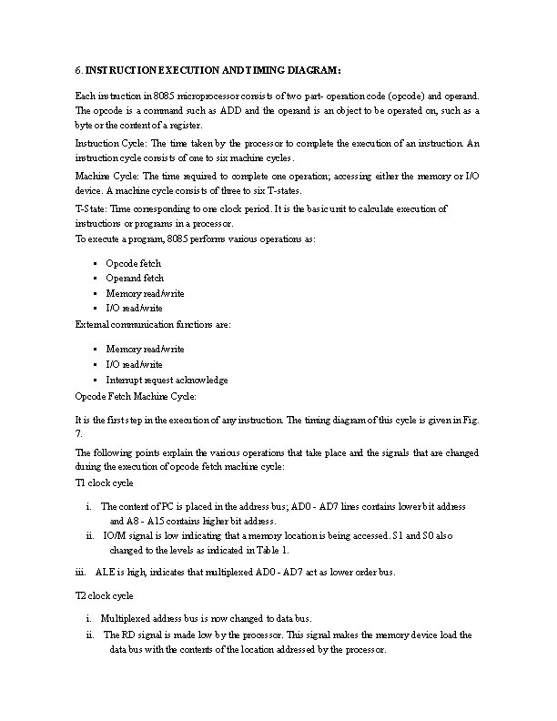
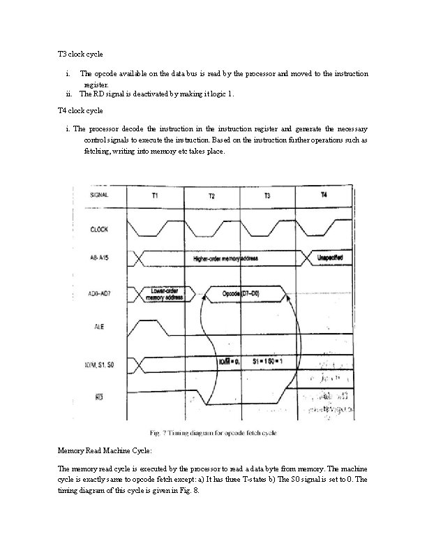
6. INSTRUCTION EXECUTION AND TIMING DIAGRAM: Each instruction in 8085 microprocessor consists of two part- operation code (opcode) and operand. The opcode is a command such as ADD and the operand is an object to be operated on, such as a byte or the content of a register. Instruction Cycle: The time taken by the processor to complete the execution of an instruction. An instruction cycle consists of one to six machine cycles. Machine Cycle: The time required to complete one operation; accessing either the memory or I/O device. A machine cycle consists of three to six T-states. T-State: Time corresponding to one clock period. It is the basic unit to calculate execution of instructions or programs in a processor. To execute a program, 8085 performs various operations as: • • Opcode fetch Operand fetch Memory read/write I/O read/write External communication functions are: • Memory read/write • I/O read/write • Interrupt request acknowledge Opcode Fetch Machine Cycle: It is the first step in the execution of any instruction. The timing diagram of this cycle is given in Fig. 7. The following points explain the various operations that take place and the signals that are changed during the execution of opcode fetch machine cycle: T 1 clock cycle i. The content of PC is placed in the address bus; AD 0 - AD 7 lines contains lower bit address and A 8 - A 15 contains higher bit address. ii. IO/M signal is low indicating that a memory location is being accessed. S 1 and S 0 also changed to the levels as indicated in Table 1. iii. ALE is high, indicates that multiplexed AD 0 - AD 7 act as lower order bus. T 2 clock cycle i. Multiplexed address bus is now changed to data bus. ii. The RD signal is made low by the processor. This signal makes the memory device load the data bus with the contents of the location addressed by the processor.

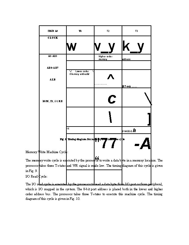
T 3 clock cycle i. ii. The opcode available on the data bus is read by the processor and moved to the instruction register. The RD signal is deactivated by making it logic 1. T 4 clock cycle i. The processor decode the instruction in the instruction register and generate the necessary control signals to execute the instruction. Based on the instruction further operations such as fetching, writing into memory etc takes place. Memory Read Machine Cycle: The memory read cycle is executed by the processor to read a data byte from memory. The machine cycle is exactly same to opcode fetch except: a) It has three T-states b) The S 0 signal is set to 0. The timing diagram of this cycle is given in Fig. 8.

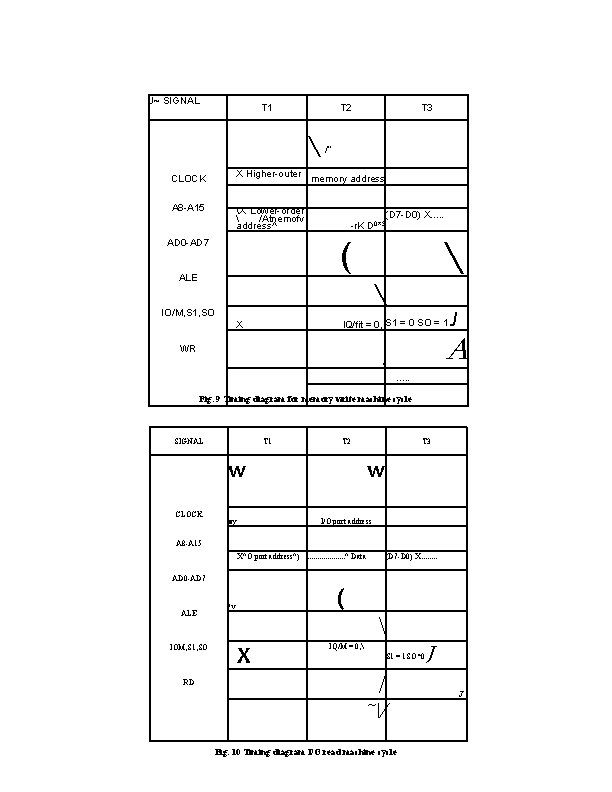
SIGN At T 1 CLOCK T 2 w T 3 v_y k_y A 5 -A 15 Higher-order memory address AD 0 -AD 7 / Lower-order /Viemory addres$/ ALE ^ . . . . (D 7 -oo). . . . ] c 10/M, S 1, SO RD ~x S 1 MS 0 -0 "77 “ Fig. 8 Timing diagram for memory read machine cycle Memory Write Machine Cycle: h -A The memory write cycle is executed by the processor to write a data byte in a memory location. The processor takes three T-states and WR signal is made low. The timing diagram of this cycle is given in Fig. 9. I/O Read Cycle: The I/O read cycle is executed by the processor to read a data byte from I/O port or from peripheral, which is I/O mapped in the system. The 8 -bit port address is placed both in the lower and higher order address bus. The processor takes three T-states to execute this machine cycle. The timing diagram of this cycle is given in Fig. 10.

J~ SIGNAL T 1 T 2 T 3 /“ CLOCK X Higher-outer memory address A 8 -A 15 X Lower-order /Atnemofv address^ (D 7 -D 0) X. . . -r. K D 0*3 ( AD 0 -AD 7 ALE IO/M, S 1, SO l. Q/fit = 0, |S 1 = 0 SO = 1 X J A WR /. . . Fig. 9 Timing diagram for memory write machine cycle SIGNAL T 1 T 2 T 3 w CLOCK ■y w I/O port address A 8 -A 15 X^O port address^). . . . . ^ Data (D 7 -D 0) X. . . . AD 0 -AD 7 ALE IOM, S 1, SO RD / v_ ( X IQ/M = 0, S 1 = 1 SO*0 / ~/ Fig. 10 Timing diagram I/O read machine cycle J J_

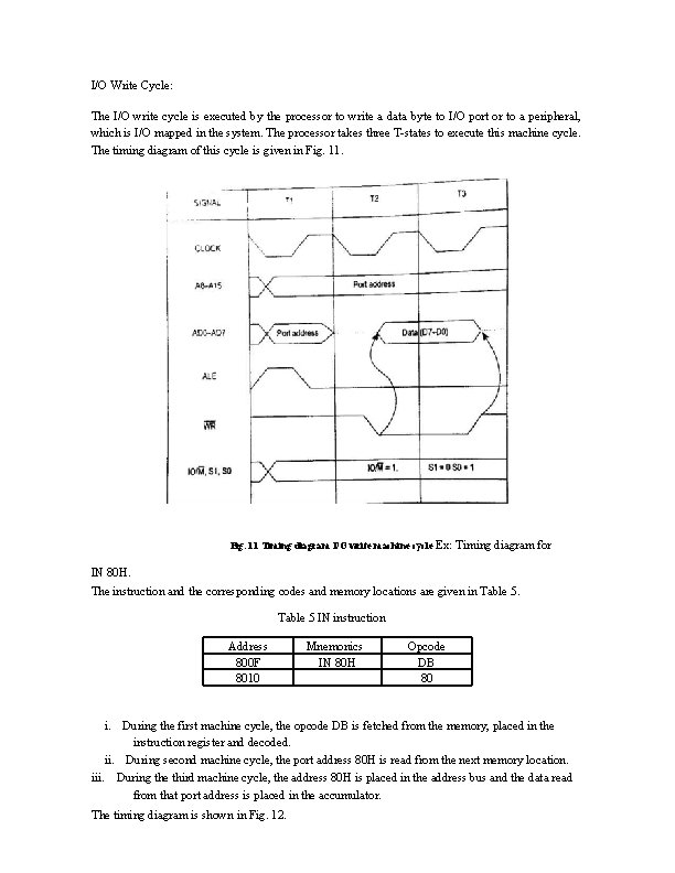
I/O Write Cycle: The I/O write cycle is executed by the processor to write a data byte to I/O port or to a peripheral, which is I/O mapped in the system. The processor takes three T-states to execute this machine cycle. The timing diagram of this cycle is given in Fig. 11 Timing diagram I/O write machine cycle Ex: Timing diagram for IN 80 H. The instruction and the corresponding codes and memory locations are given in Table 5 IN instruction Address 800 F 8010 i. Mnemonics IN 80 H Opcode DB 80 During the first machine cycle, the opcode DB is fetched from the memory, placed in the instruction register and decoded. ii. During second machine cycle, the port address 80 H is read from the next memory location. iii. During the third machine cycle, the address 80 H is placed in the address bus and the data read from that port address is placed in the accumulator. The timing diagram is shown in Fig. 12.