Kharkov National University of Radioelectronics Kharkov Ukraine April

- Slides: 96

Kharkov National University of Radioelectronics Kharkov, Ukraine April 5 -7, 2004 Test Generation and Fault Simulation for Digital Systems Raimund Ubar Tallinn Technical University D&T Laboratory Estonia 1 Copyright 2000 -2003 by Raimund Ubar Technical University Tallinn, ESTONIA

Motivation of the Course • The increasing complexity of VLSI circuits has made test generation one of the most complicated and time-consuming problems in digital design • The more complex are getting systems, the more important will be the problems of test and design for testability because of the very high cost of testing electronic products • Engineers involved in So. C design and technology should be – made better aware of the importance of test, – very close relationships between design and test, and – trained in test technology to enable them to design and produce high quality, defect-free and fault-tolerant products 2 Copyright 2000 -2003 by Raimund Ubar Technical University Tallinn, ESTONIA

Goals of the Course • The main goal of the course is to give the basic knowledge to answer the question: How to improve the testing quality at increasing complexities of today's systems? • This knowledges includes – understanding of how the physical defects can influence on the behavior of systems, and how the fault modelling can be carried out – learning the basic techniques of fault simulation, test generation and fault diagnosis – understanding the meaning of testability, and how the testability of a system can be measured and improved – learning the basic methods of making systems self-testable • The goal is also to give some hands-on experience of solving test related problems 3 Copyright 2000 -2003 by Raimund Ubar Technical University Tallinn, ESTONIA

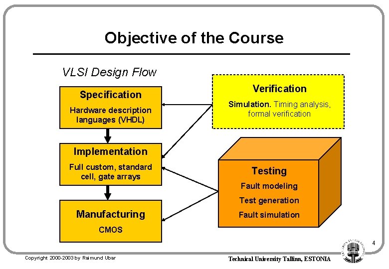
Objective of the Course VLSI Design Flow Specification Hardware description languages (VHDL) Verification Simulation. Timing analysis, formal verification Implementation Full custom, standard cell, gate arrays Testing Fault modeling Test generation Manufacturing Fault simulation CMOS 4 Copyright 2000 -2003 by Raimund Ubar Technical University Tallinn, ESTONIA

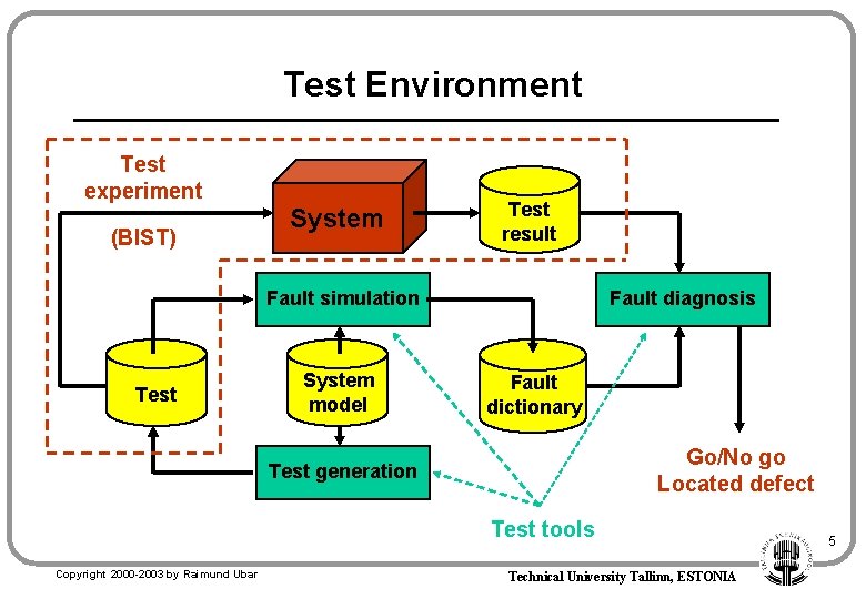
Test Environment Test experiment (BIST) System Test result Fault simulation Test System model Fault diagnosis Fault dictionary Go/No go Located defect Test generation Test tools Copyright 2000 -2003 by Raimund Ubar Technical University Tallinn, ESTONIA 5

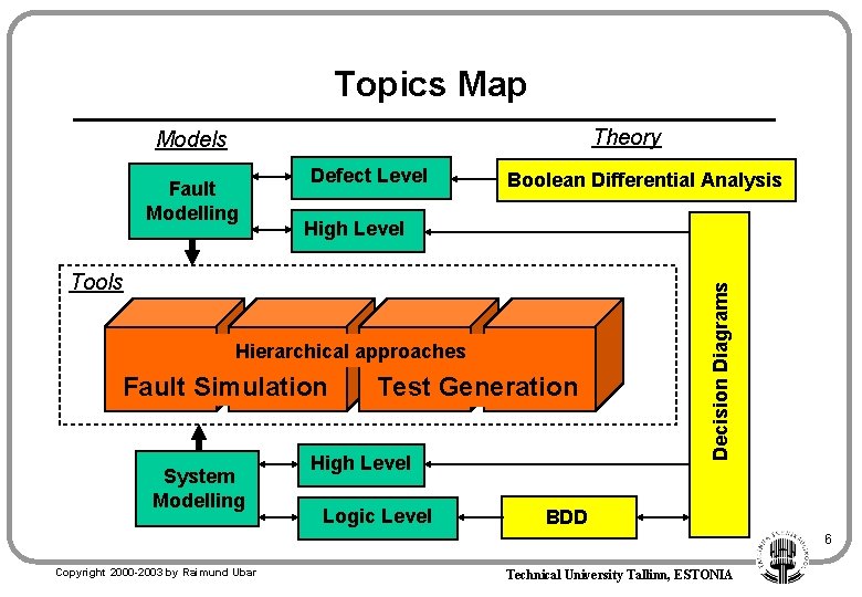
Topics Map Theory Models Defect Level Boolean Differential Analysis High Level Tools Hierarchical approaches Fault Simulation System Modelling Test Generation High Level Logic Level Decision Diagrams Fault Modelling BDD 6 Copyright 2000 -2003 by Raimund Ubar Technical University Tallinn, ESTONIA

Abstract • • How to improve the testing quality at increasing complexities of today's systems? Two main trends: defect-oriented test and high-level modelling – Both are caused by the increasing complexities of systems based on deepsubmicron technologies • • • The complexity problems in testing digital systems are handled by raising the abstraction levels from gate to register-transfer level (RTL) instruction set architecture (ISA) or behavioral levels To handle defects in circuits implemented in deep-submicron technologies, new fault models and defect-oriented test methods should be used Trends to high-level modelling and defect-orientation are opposite As a promising compromise and solution is: to combine hierarchical approach with defect orientation Decision Diagrams serve as a good tool for hierarchical modelling of defects in digital systems 7 Copyright 2000 -2003 by Raimund Ubar Technical University Tallinn, ESTONIA

Outline • Introduction to Digital Test (5) • How to improve test quality at increasing complexity of systems (9) • High-level modelling and defect-orientation (25) • BDDs and logic level testing • Hierarchical test generation (42) – General concepts – Test generation for RT Level systems – Test generation for Microprocessors • Hierarchical fault simulation (62) • Overview of tools developed at D&T Lab (70) 8 Copyright 2000 -2003 by Raimund Ubar Technical University Tallinn, ESTONIA

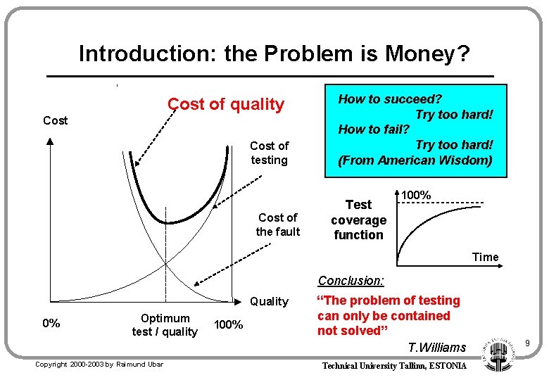
Introduction: the Problem is Money? Cost of quality Cost of testing Cost of the fault How to succeed? Try too hard! How to fail? Try too hard! (From American Wisdom) Test coverage function 100% Time Conclusion: Quality 0% Optimum test / quality Copyright 2000 -2003 by Raimund Ubar 100% “The problem of testing can only be contained not solved” T. Williams Technical University Tallinn, ESTONIA 9

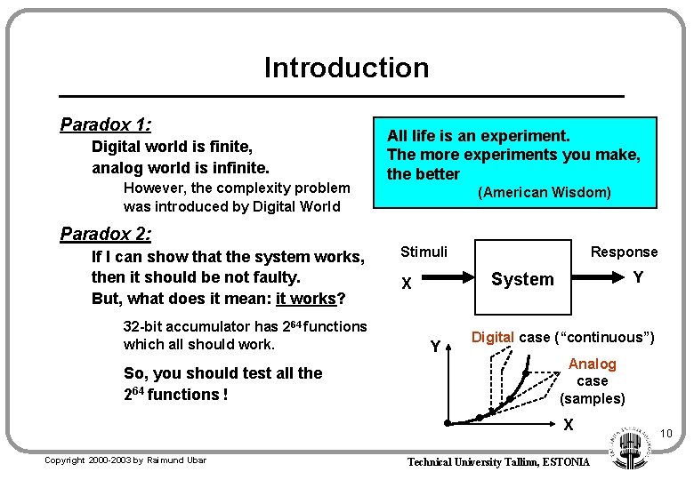
Introduction Paradox 1: Digital world is finite, analog world is infinite. However, the complexity problem was introduced by Digital World Paradox 2: If I can show that the system works, then it should be not faulty. But, what does it mean: it works? 32 -bit accumulator has 264 functions which all should work. So, you should test all the 264 functions ! All life is an experiment. The more experiments you make, the better (American Wisdom) Stimuli Response Y System X Y Digital case (“continuous”) Analog case (samples) X Copyright 2000 -2003 by Raimund Ubar Technical University Tallinn, ESTONIA 10

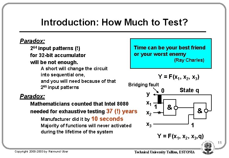
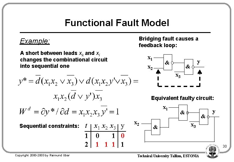
Introduction: How Much to Test? Paradox: Time can be your best friend or your worst enemy 264 input patterns (!) for 32 -bit accumulator will be not enough. A short will change the circuit into sequential one, and you will need because of that 265 input patterns (Ray Charles) Y = F(x 1, x 2, x 3) Bridging fault Paradox: Mathematicians counted that Intel 8080 needed for exhaustive testing 37 (!) years Manufacturer did it by 10 seconds Majority of functions will never activated during the lifetime of the system y x 1 x 2 x 3 State q 0 1 * & & 1 Y = F(x 1, x 2, x 3, q) 11 Copyright 2000 -2003 by Raimund Ubar Technical University Tallinn, ESTONIA

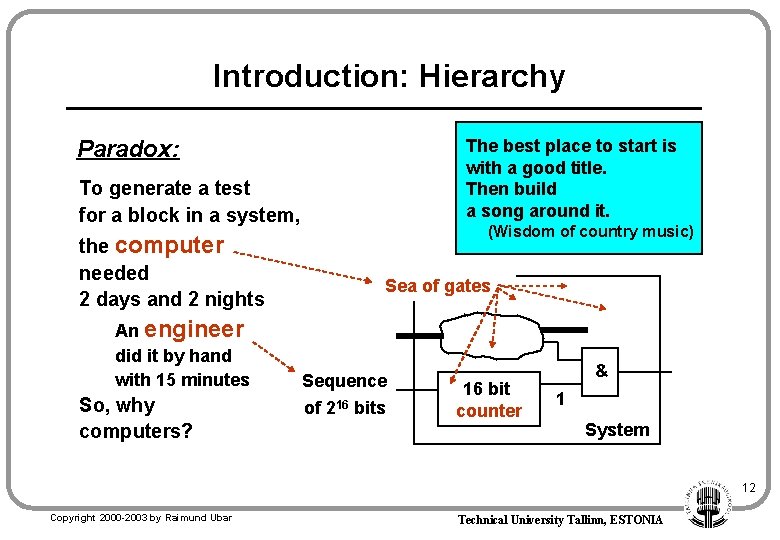
Introduction: Hierarchy Paradox: The best place to start is with a good title. Then build a song around it. To generate a test for a block in a system, the computer needed 2 days and 2 nights An engineer did it by hand with 15 minutes So, why computers? (Wisdom of country music) Sea of gates Sequence of 216 bits 16 bit counter & 1 System 12 Copyright 2000 -2003 by Raimund Ubar Technical University Tallinn, ESTONIA

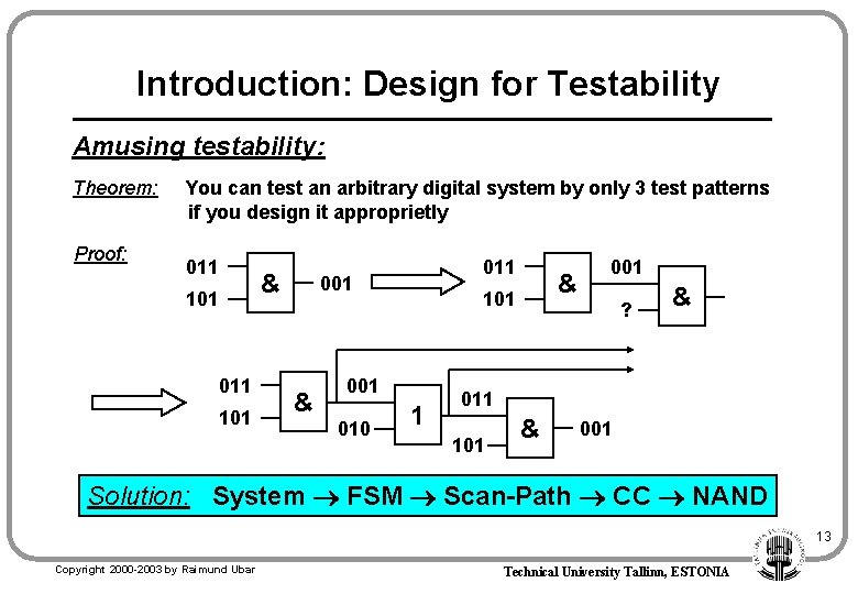
Introduction: Design for Testability Amusing testability: Theorem: Proof: You can test an arbitrary digital system by only 3 test patterns if you design it approprietly 011 101 & 011 001 & 001 010 & 101 1 001 ? & 011 101 & 001 Solution: System FSM Scan-Path CC NAND 13 Copyright 2000 -2003 by Raimund Ubar Technical University Tallinn, ESTONIA

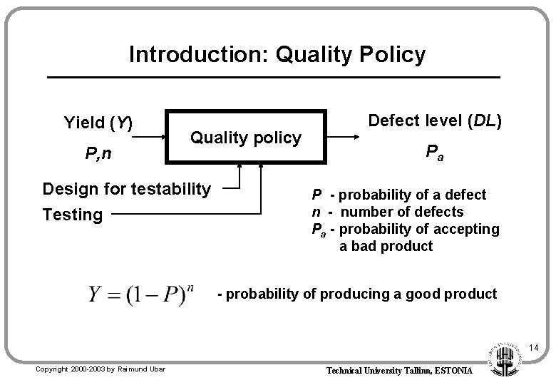
Introduction: Quality Policy Yield (Y) P, n Quality policy Design for testability Testing Defect level (DL) Pa P - probability of a defect n - number of defects Pa - probability of accepting a bad product - probability of producing a good product 14 Copyright 2000 -2003 by Raimund Ubar Technical University Tallinn, ESTONIA

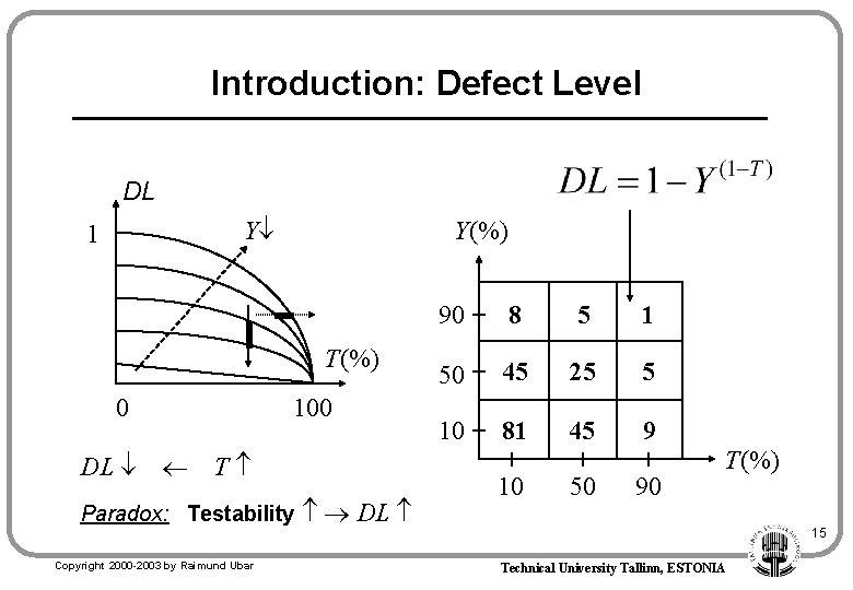
Introduction: Defect Level DL Y 1 Y(%) T(%) 0 DL 100 T Paradox: Testability Copyright 2000 -2003 by Raimund Ubar DL 90 8 5 1 50 45 25 5 10 81 45 9 10 50 90 T(%) 15 Technical University Tallinn, ESTONIA

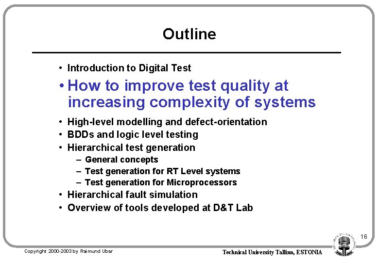
Outline • Introduction to Digital Test • How to improve test quality at increasing complexity of systems • High-level modelling and defect-orientation • BDDs and logic level testing • Hierarchical test generation – General concepts – Test generation for RT Level systems – Test generation for Microprocessors • Hierarchical fault simulation • Overview of tools developed at D&T Lab 16 Copyright 2000 -2003 by Raimund Ubar Technical University Tallinn, ESTONIA

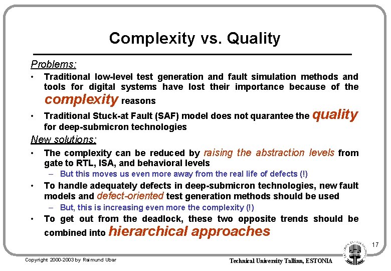
Complexity vs. Quality Problems: • Traditional low-level test generation and fault simulation methods and tools for digital systems have lost their importance because of the complexity reasons • Traditional Stuck-at Fault (SAF) model does not quarantee the quality for deep-submicron technologies New solutions: • The complexity can be reduced by raising the abstraction levels from gate to RTL, ISA, and behavioral levels – But this moves us even more away from the real life of defects (!) • To handle adequately defects in deep-submicron technologies, new fault models and defect-oriented test generation methods should be used – But, this is increasing even more the complexity (!) • To get out from the deadlock, these two opposite trends should be combined into hierarchical approaches 17 Copyright 2000 -2003 by Raimund Ubar Technical University Tallinn, ESTONIA

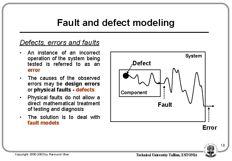
Fault and defect modeling Defects, errors and faults • • An instance of an incorrect operation of the system being tested is referred to as an error The causes of the observed errors may be design errors or physical faults - defects Physical faults do not allow a direct mathematical treatment of testing and diagnosis The solution is to deal with fault models System Defect Component Fault Error 18 Copyright 2000 -2003 by Raimund Ubar Technical University Tallinn, ESTONIA

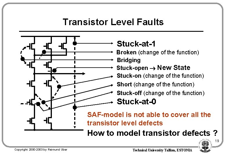
Transistor Level Faults Stuck-at-1 Broken (change of the function) Bridging Stuck-open New State Stuck-on (change of the function) Short (change of the function) Stuck-off (change of the function) Stuck-at-0 SAF-model is not able to cover all the transistor level defects How to model transistor defects ? 19 Copyright 2000 -2003 by Raimund Ubar Technical University Tallinn, ESTONIA

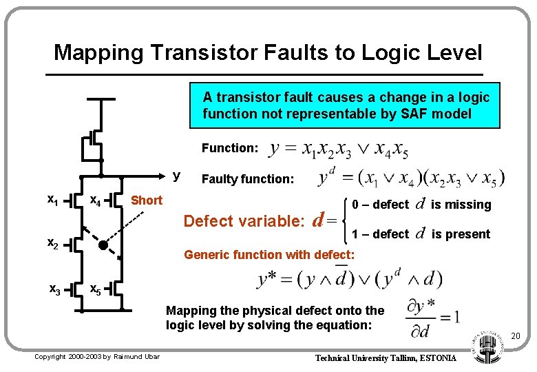
Mapping Transistor Faults to Logic Level A transistor fault causes a change in a logic function not representable by SAF model Function: y x 1 x 4 Faulty function: Short Defect variable: x 2 x 3 d= 0 – defect d is missing 1 – defect d is present Generic function with defect: x 5 Mapping the physical defect onto the logic level by solving the equation: Copyright 2000 -2003 by Raimund Ubar Technical University Tallinn, ESTONIA 20

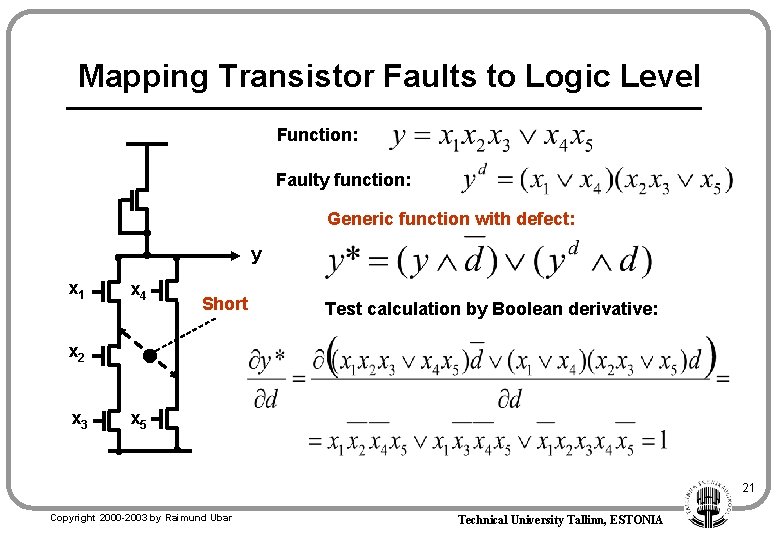
Mapping Transistor Faults to Logic Level Function: Faulty function: Generic function with defect: y x 1 x 4 Short Test calculation by Boolean derivative: x 2 x 3 x 5 21 Copyright 2000 -2003 by Raimund Ubar Technical University Tallinn, ESTONIA

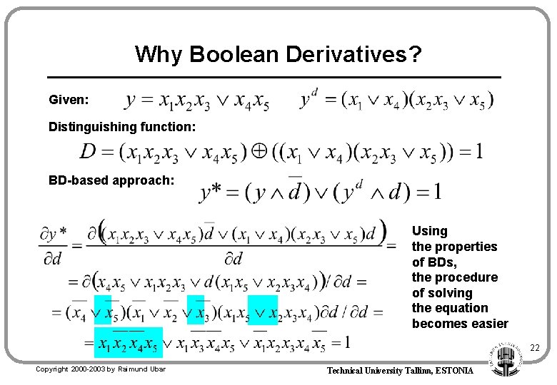
Why Boolean Derivatives? Given: Distinguishing function: BD-based approach: Using the properties of BDs, the procedure of solving the equation becomes easier 22 Copyright 2000 -2003 by Raimund Ubar Technical University Tallinn, ESTONIA

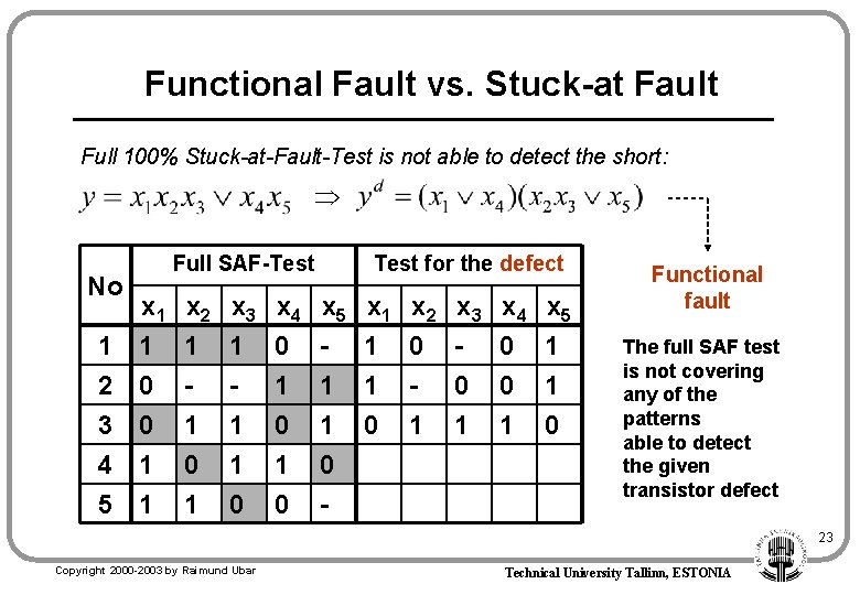
Functional Fault vs. Stuck-at Fault Full 100% Stuck-at-Fault-Test is not able to detect the short: No Full SAF-Test for the defect x 1 x 2 x 3 x 4 x 5 1 1 0 - 0 1 2 0 - - 1 1 1 - 0 0 1 3 0 4 1 5 1 1 0 1 1 1 0 0 1 0 - 0 1 1 1 0 Functional fault The full SAF test is not covering any of the patterns able to detect the given transistor defect 23 Copyright 2000 -2003 by Raimund Ubar Technical University Tallinn, ESTONIA

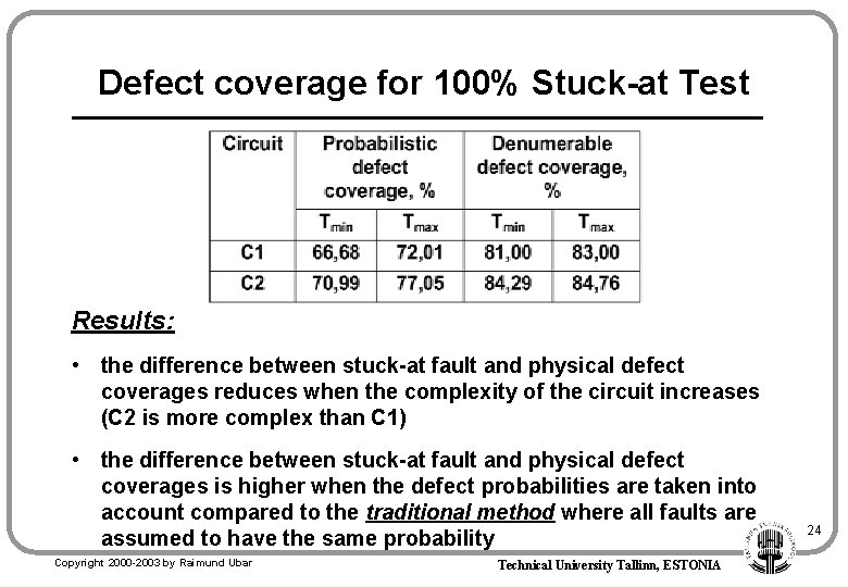
Defect coverage for 100% Stuck-at Test Results: • the difference between stuck-at fault and physical defect coverages reduces when the complexity of the circuit increases (C 2 is more complex than C 1) • the difference between stuck-at fault and physical defect coverages is higher when the defect probabilities are taken into account compared to the traditional method where all faults are assumed to have the same probability Copyright 2000 -2003 by Raimund Ubar Technical University Tallinn, ESTONIA 24

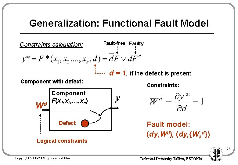
Generalization: Functional Fault Model Constraints calculation: Fault-free Faulty d = 1, if the defect is present Component with defect: Wd Component F(x 1, x 2, …, xn) Defect Logical constraints Constraints: y Fault model: (dy, Wd), (dy, {Wkd}) 25 Copyright 2000 -2003 by Raimund Ubar Technical University Tallinn, ESTONIA

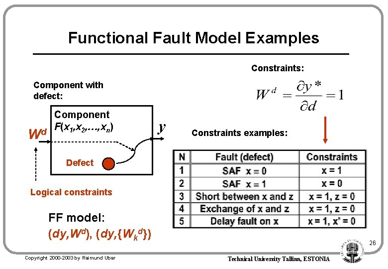
Functional Fault Model Examples Constraints: Component with defect: Wd Component F(x 1, x 2, …, xn) y Constraints examples: Defect Logical constraints FF model: (dy, Wd), (dy, {Wkd}) Copyright 2000 -2003 by Raimund Ubar 26 Technical University Tallinn, ESTONIA

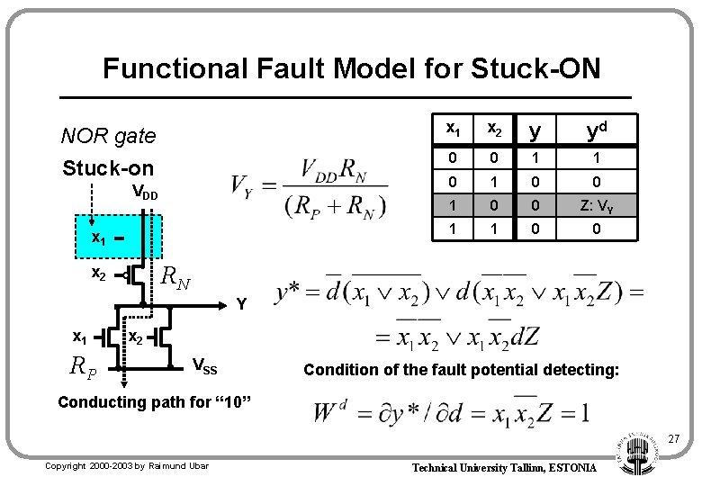
Functional Fault Model for Stuck-ON NOR gate Stuck-on VDD x 1 x 2 y yd 0 0 1 1 0 0 Z: VY 1 1 0 0 RN x 2 Y x 1 RP x 2 VSS Condition of the fault potential detecting: Conducting path for “ 10” 27 Copyright 2000 -2003 by Raimund Ubar Technical University Tallinn, ESTONIA

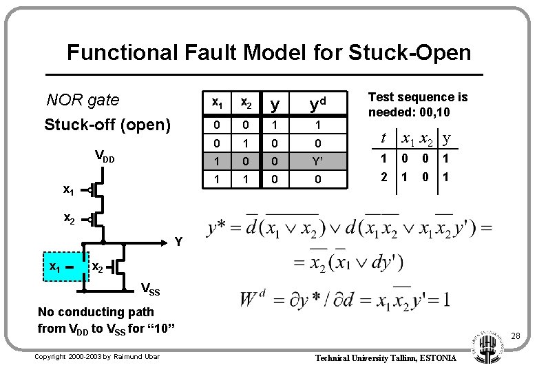
Functional Fault Model for Stuck-Open NOR gate Stuck-off (open) VDD x 1 Test sequence is needed: 00, 10 x 1 x 2 y yd 0 0 1 1 0 0 t x 1 x 2 y 1 0 0 Y’ 1 0 0 1 1 1 0 0 2 1 0 1 x 2 Y x 1 x 2 VSS No conducting path from VDD to VSS for “ 10” Copyright 2000 -2003 by Raimund Ubar 28 Technical University Tallinn, ESTONIA

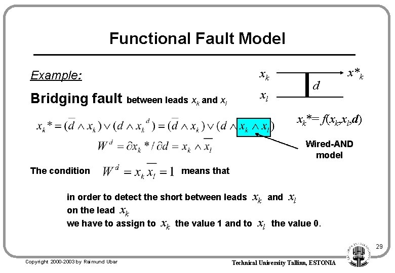
Functional Fault Model Example: xk Bridging fault between leads xk and xl xl d x*k xk*= f(xk, xl, d) Wired-AND model The condition means that in order to detect the short between leads xk and xl on the lead xk we have to assign to xk the value 1 and to xl the value 0. 29 Copyright 2000 -2003 by Raimund Ubar Technical University Tallinn, ESTONIA

Functional Fault Model Bridging fault causes a feedback loop: Example: A short between leads xk and xl changes the combinational circuit into sequential one x 1 & x 2 y & x 3 Equivalent faulty circuit: x 1 Sequential constraints: Copyright 2000 -2003 by Raimund Ubar t x 1 x 2 x 3 y 1 0 2 1 1 x 2 & & & y x 3 30 Technical University Tallinn, ESTONIA

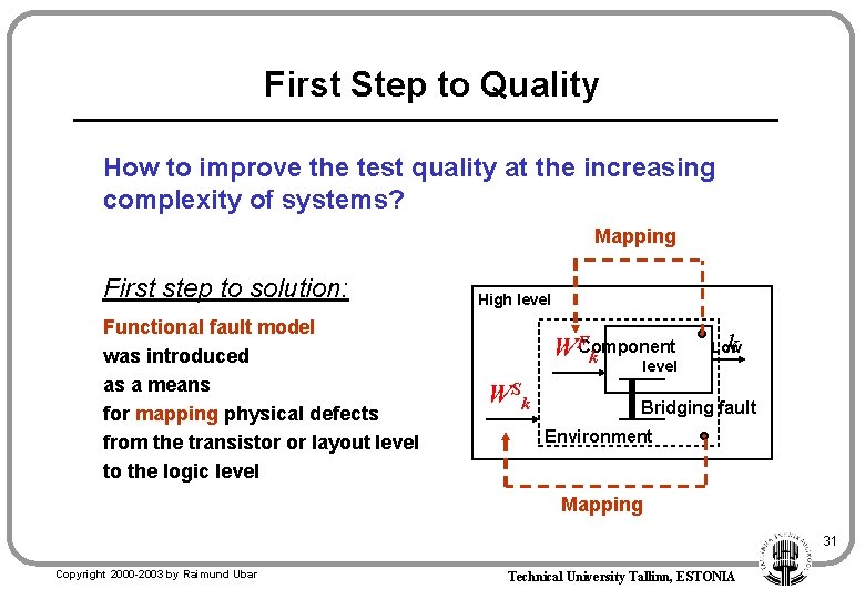
First Step to Quality How to improve the test quality at the increasing complexity of systems? Mapping First step to solution: Functional fault model was introduced as a means for mapping physical defects from the transistor or layout level to the logic level High level System WFComponent k level W Sk k Low Bridging fault Environment Mapping 31 Copyright 2000 -2003 by Raimund Ubar Technical University Tallinn, ESTONIA

Outline • Introduction to Digital Test • How to improve test quality at increasing complexity of systems • High-level modelling and defectorientation • BDDs and logic level testing • Hierarchical test generation – General concepts – Test generation for RT Level systems – Test generation for Microprocessors • Hierarchical fault simulation • Overview of tools developed at D&T Lab 32 Copyright 2000 -2003 by Raimund Ubar Technical University Tallinn, ESTONIA

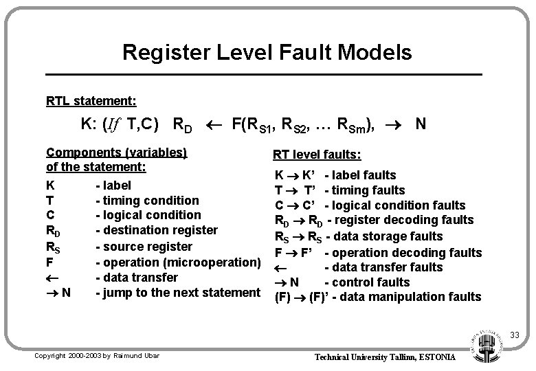
Register Level Fault Models RTL statement: K: (If T, C) RD F(RS 1, RS 2, … RSm), N Components (variables) RT level faults: of the statement: K K’ - label faults K - label T T’ - timing faults T - timing condition C C’ - logical condition faults C - logical condition RD - register decoding faults RD - destination register RS - data storage faults RS - source register F F’ - operation decoding faults F - operation (microoperation) - data transfer faults - data transfer N - control faults N - jump to the next statement (F)’ - data manipulation faults 33 Copyright 2000 -2003 by Raimund Ubar Technical University Tallinn, ESTONIA

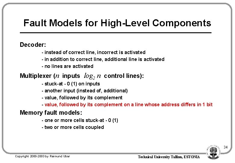
Fault Models for High-Level Components Decoder: - instead of correct line, incorrect is activated - in addition to correct line, additional line is activated - no lines are activated Multiplexer (n inputs log 2 n control lines): - stuck-at - 0 (1) on inputs - another input (instead of, additional) - value, followed by its complement on a line whose address differs in 1 bit Memory fault models: - one or more cells stuck-at - 0 (1) - two or more cells coupled 34 Copyright 2000 -2003 by Raimund Ubar Technical University Tallinn, ESTONIA

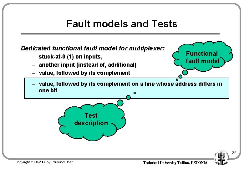
Fault models and Tests Dedicated functional fault model for multiplexer: – stuck-at-0 (1) on inputs, – another input (instead of, additional) – value, followed by its complement Functional fault model – value, followed by its complement on a line whose address differs in one bit Test description 35 Copyright 2000 -2003 by Raimund Ubar Technical University Tallinn, ESTONIA

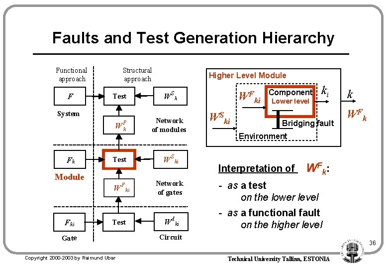
Faults and Test Generation Hierarchy Functional approach F Structural approach Test System Fk Network of modules Test W S ki W F ki Network of gates Test Gate Copyright 2000 -2003 by Raimund Ubar WFki W Sk W Fk Module F ki Higher Level Module W d ki WSki Component Lower level ki Bridging fault k WF k Environment Interpretation of W F k: - as a test on the lower level - as a functional fault on the higher level Circuit 36 Technical University Tallinn, ESTONIA

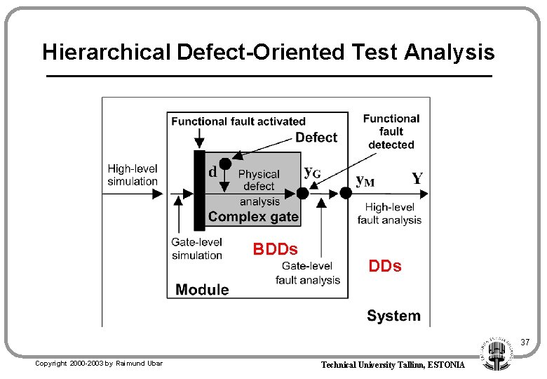
Hierarchical Defect-Oriented Test Analysis BDDs 37 Copyright 2000 -2003 by Raimund Ubar Technical University Tallinn, ESTONIA

Outline • Introduction to Digital Test • How to improve test quality at increasing complexity of systems • High-level modelling and defect-orientation • BDDs and logic level testing • Hierarchical test generation – General concepts – Test generation for RT Level systems – Test generation for Microprocessors • Hierarchical fault simulation • Overview of tools developed at D&T Lab 38 Copyright 2000 -2003 by Raimund Ubar Technical University Tallinn, ESTONIA

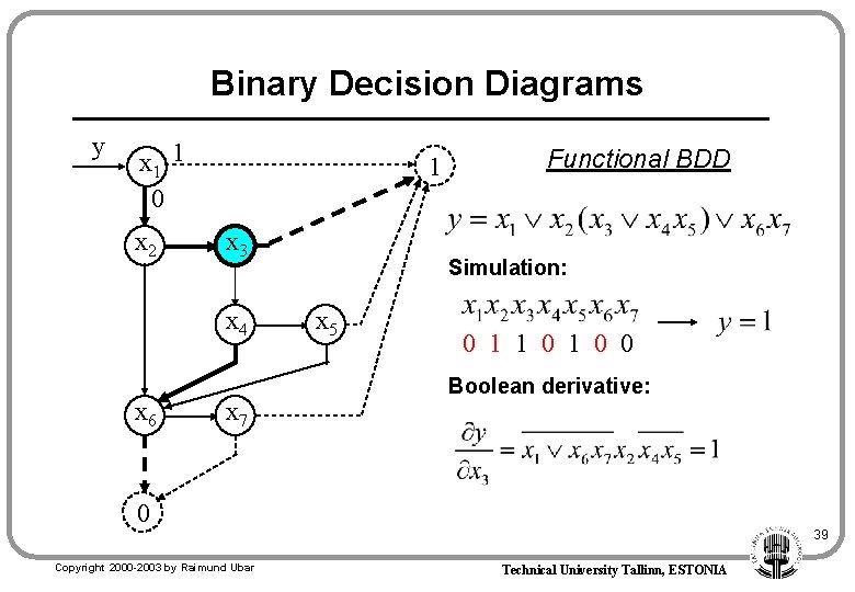
Binary Decision Diagrams y x 1 1 0 x 2 1 x 3 x 4 x 6 x 7 Functional BDD Simulation: x 5 0 1 1 0 0 Boolean derivative: 0 39 Copyright 2000 -2003 by Raimund Ubar Technical University Tallinn, ESTONIA

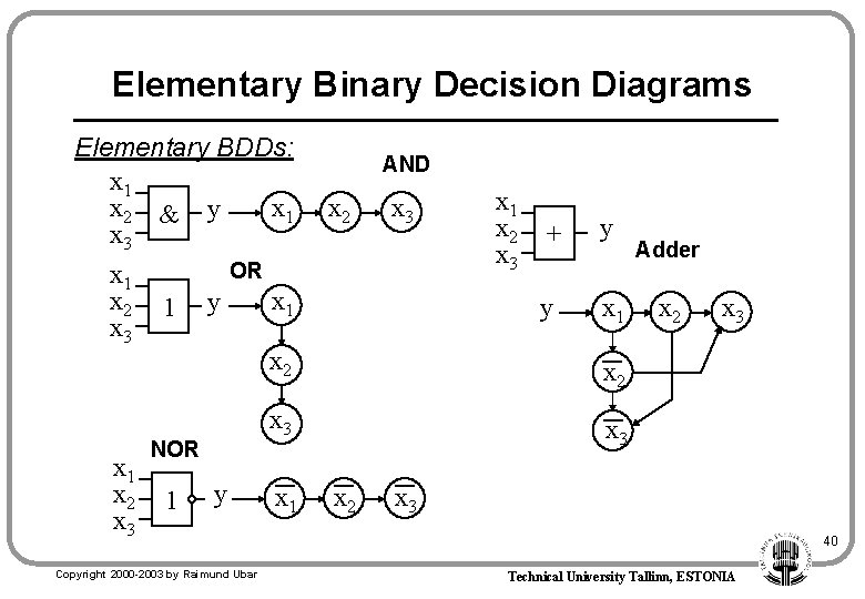
Elementary Binary Decision Diagrams Elementary BDDs: x 1 x 2 & y x 1 x 3 OR x 1 x 2 1 y x 1 x 3 x 2 x 1 x 2 x 3 y Copyright 2000 -2003 by Raimund Ubar x 1 x 2 x 3 + y y x 1 Adder x 2 x 3 NOR 1 AND x 3 x 2 x 3 40 Technical University Tallinn, ESTONIA

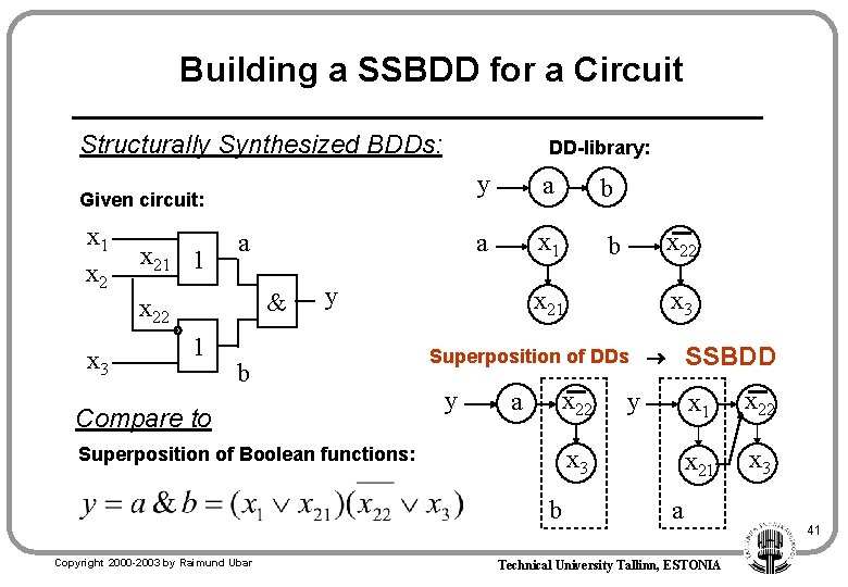
Building a SSBDD for a Circuit Structurally Synthesized BDDs: DD-library: Given circuit: x 1 x 21 1 a & x 22 x 3 1 y a b a x 1 b y b Compare to x 21 x 3 SSBDD Superposition of DDs y x 22 a Superposition of Boolean functions: y x 3 b Copyright 2000 -2003 by Raimund Ubar x 22 x 1 x 22 x 21 x 3 a Technical University Tallinn, ESTONIA 41

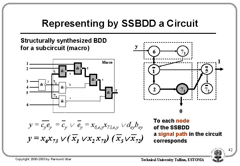
Representing by SSBDD a Circuit Structurally synthesized BDD for a subcircuit (macro) 4 5 6 6 73 1 Macro 1 2 3 y 71 & 7 & & d & 72 & e b & 73 & 5 1 a 2 y 71 72 c 0 y = cyey = cy ey = x 6, e, yx 73, e, y deybey y = x 6 x 73 ( x 1 x 2 x 71) ( x 5 x 72) To each node of the SSBDD a signal path in the circuit corresponds 42 Copyright 2000 -2003 by Raimund Ubar Technical University Tallinn, ESTONIA

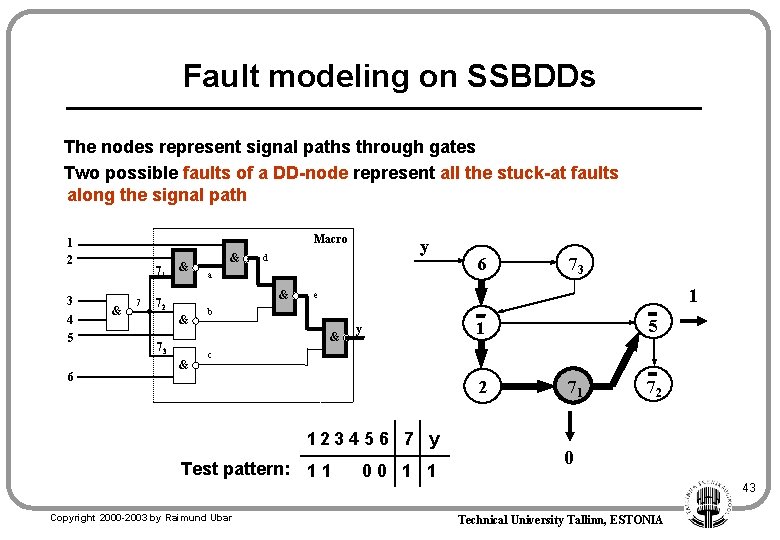
Fault modeling on SSBDDs The nodes represent signal paths through gates Two possible faults of a DD-node represent all the stuck-at faults along the signal path Macro 1 2 3 4 5 6 71 & 7 & & a & 72 & & 6 73 1 e b & 73 y d y 5 1 c 2 123 4 5 6 7 y Test pattern: 1 1 00 1 1 71 72 0 43 Copyright 2000 -2003 by Raimund Ubar Technical University Tallinn, ESTONIA

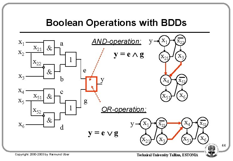
Boolean Operations with BDDs x 1 x 21 & & x 3 x 4 x 51 & y b c 1 & x 1 x 22 x 21 x 3 x 4 x 52 x 51 x 6 e x 52 x 6 y=e g 1 x 22 y AND-operation: a d Copyright 2000 -2003 by Raimund Ubar g OR-operation: y=e g y x 1 x 22 x 4 x 52 x 21 x 3 x 51 x 6 Technical University Tallinn, ESTONIA 44

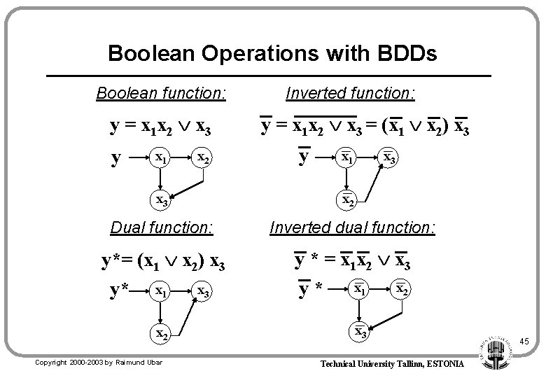
Boolean Operations with BDDs Boolean function: y = x 1 x 2 x 3 y x 1 x 2 x 3 Inverted function: y = x 1 x 2 x 3 = (x 1 x 2) x 3 y x 1 x 3 x 2 Dual function: Inverted dual function: y*= (x 1 x 2) x 3 y* x 1 y * = x 1 x 2 x 3 x 1 x 2 y* x 2 Copyright 2000 -2003 by Raimund Ubar x 3 Technical University Tallinn, ESTONIA 45

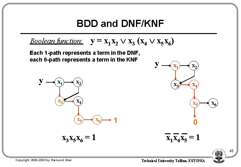
BDD and DNF/KNF Boolean function: y = x 1 x 2 x 3 (x 4 x 5 x 6) Each 1 -path represents a term in the DNF, each 0 -path represents a term in the KNF y x 1 x 2 x 3 x 4 x 5 x 6 x 3 x 5 x 6 = 1 1 x 6 0 x 1 x 4 x 5 = 1 46 Copyright 2000 -2003 by Raimund Ubar Technical University Tallinn, ESTONIA

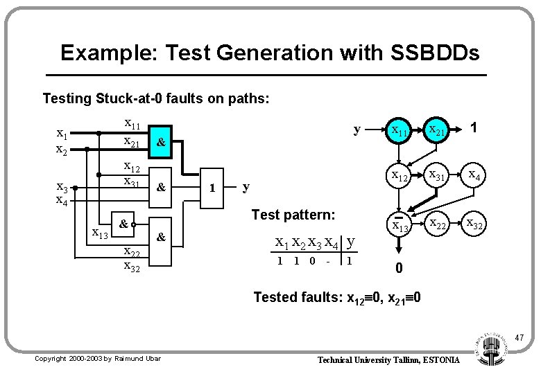
Example: Test Generation with SSBDDs Testing Stuck-at-0 faults on paths: x 11 x 21 x 2 x 12 x 31 x 3 x 4 x 13 & x 22 x 32 y & & 1 y Test pattern: & x 1 x 2 x 3 x 4 y 1 1 0 - 1 x 11 x 21 1 x 12 x 31 x 4 x 13 x 22 x 32 0 Tested faults: x 12 0, x 21 0 47 Copyright 2000 -2003 by Raimund Ubar Technical University Tallinn, ESTONIA

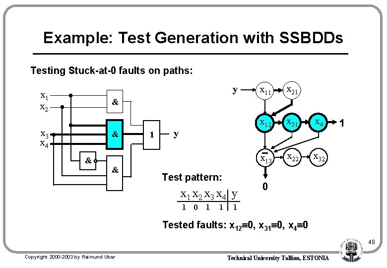
Example: Test Generation with SSBDDs Testing Stuck-at-0 faults on paths: y x 1 x 2 x 11 x 21 x 12 x 31 x 4 x 13 x 22 x 32 & x 3 x 4 & & & 1 y Test pattern: x 1 x 2 x 3 x 4 y 1 0 1 1 1 0 1 Tested faults: x 12 0, x 31 0, x 4 0 48 Copyright 2000 -2003 by Raimund Ubar Technical University Tallinn, ESTONIA

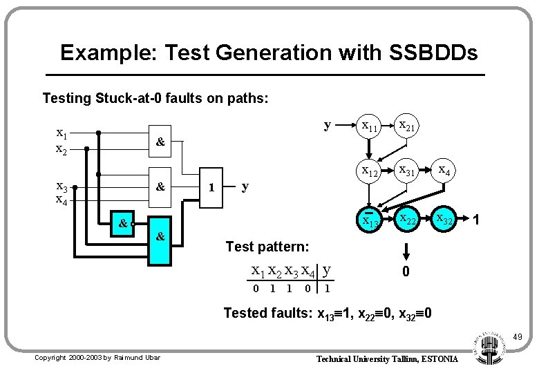
Example: Test Generation with SSBDDs Testing Stuck-at-0 faults on paths: y x 1 x 2 x 11 x 21 x 12 x 31 x 4 x 13 x 22 x 32 & x 3 x 4 & & & 1 y 1 Test pattern: x 1 x 2 x 3 x 4 y 0 1 1 0 0 1 Tested faults: x 13 1, x 22 0, x 32 0 49 Copyright 2000 -2003 by Raimund Ubar Technical University Tallinn, ESTONIA

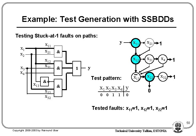
Example: Test Generation with SSBDDs Testing Stuck-at-1 faults on paths: x 11 x 21 x 2 x 12 x 31 x 3 x 4 x 13 & x 22 x 32 y x 11 x 21 x 12 x 31 x 4 1 x 13 x 22 x 32 1 1 & & 1 y Test pattern: & x 1 x 2 x 3 x 4 y 0 0 1 1 0 0 Tested faults: x 11 1, x 12 1, x 22 1 50 Copyright 2000 -2003 by Raimund Ubar Technical University Tallinn, ESTONIA

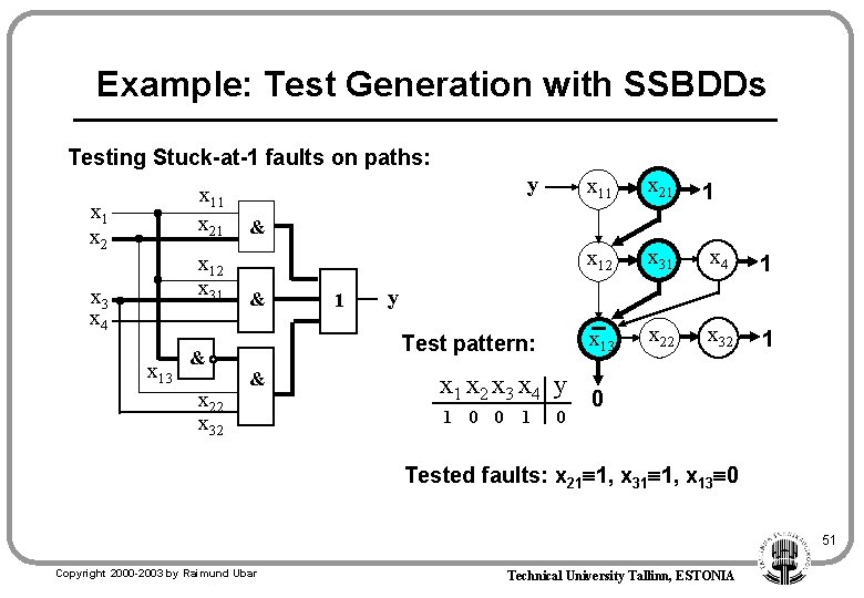
Example: Test Generation with SSBDDs Testing Stuck-at-1 faults on paths: x 11 x 21 x 2 x 12 x 31 x 3 x 4 x 13 & x 22 x 32 y x 11 x 21 x 12 x 31 x 4 1 x 13 x 22 x 32 1 1 & & 1 y Test pattern: & x 1 x 2 x 3 x 4 y 1 0 0 Tested faults: x 21 1, x 31 1, x 13 0 51 Copyright 2000 -2003 by Raimund Ubar Technical University Tallinn, ESTONIA

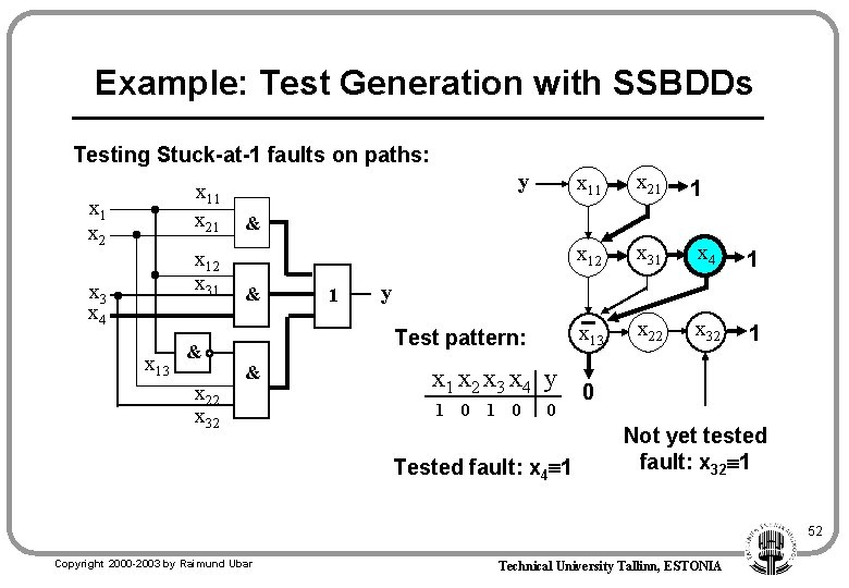
Example: Test Generation with SSBDDs Testing Stuck-at-1 faults on paths: x 11 x 21 x 2 x 12 x 31 x 3 x 4 x 13 & x 22 x 32 y x 11 x 21 x 12 x 31 x 4 1 x 13 x 22 x 32 1 1 & & 1 y Test pattern: & x 1 x 2 x 3 x 4 y 1 0 0 Tested fault: x 4 1 0 Not yet tested fault: x 32 1 52 Copyright 2000 -2003 by Raimund Ubar Technical University Tallinn, ESTONIA

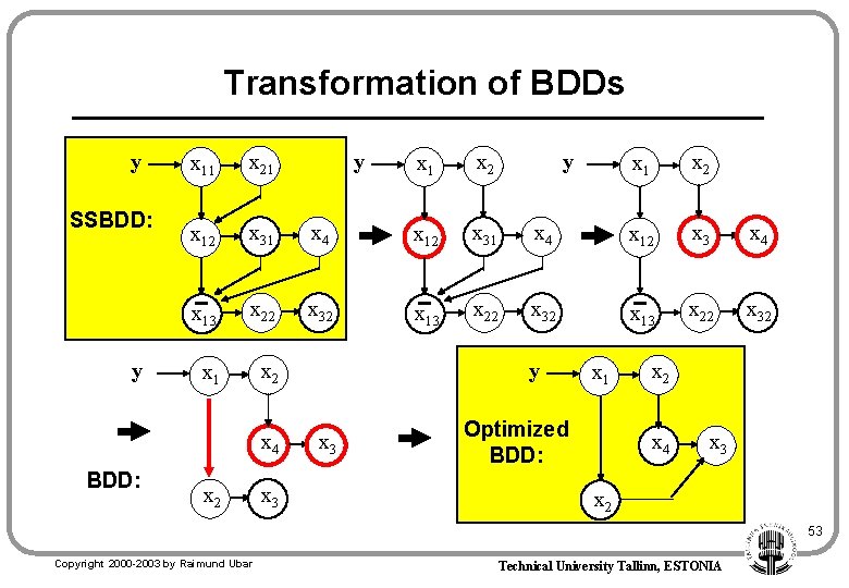
Transformation of BDDs y SSBDD: y x 11 x 21 x 12 x 31 x 13 x 22 x 1 x 2 x 4 BDD: x 2 x 3 y y x 1 x 2 x 4 x 12 x 31 x 32 x 13 x 22 x 1 x 2 x 4 x 12 x 3 x 4 x 32 x 13 x 22 x 32 y x 3 x 1 Optimized BDD: x 2 x 4 x 3 x 2 53 Copyright 2000 -2003 by Raimund Ubar Technical University Tallinn, ESTONIA

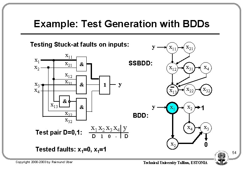
Example: Test Generation with BDDs Testing Stuck-at faults on inputs: x 1 x 2 x 3 x 4 x 13 x 11 x 21 & x 12 x 31 & & x 22 x 32 SSBDD: 1 y y & Test pair D=0, 1: x 11 x 21 x 12 x 31 x 4 x 13 x 22 x 32 x 1 x 2 1 BDD: x 1 x 2 x 3 x 4 y D 1 0 - Tested faults: x 1 0, x 1 1 Copyright 2000 -2003 by Raimund Ubar y x 4 x 3 D x 2 0 54 Technical University Tallinn, ESTONIA

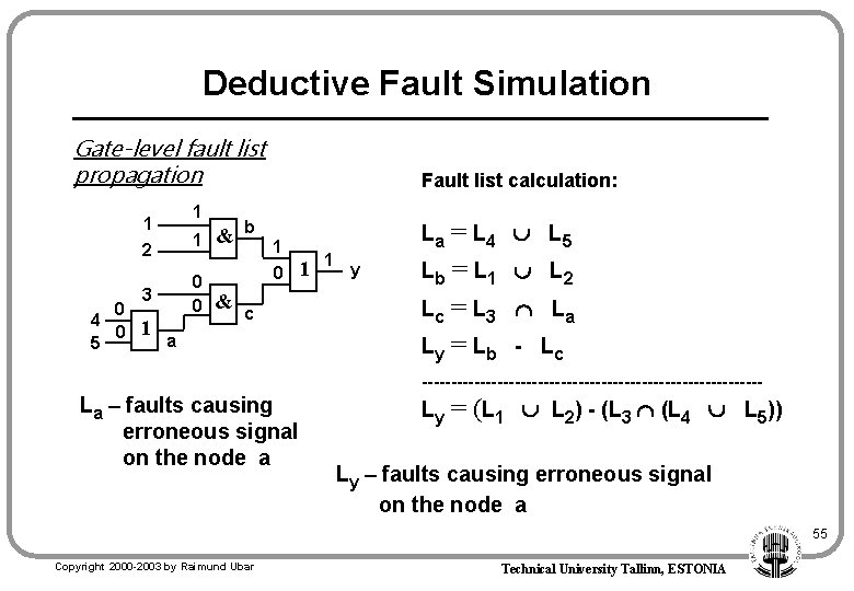
Deductive Fault Simulation Gate-level fault list propagation 1 1 2 0 4 0 5 1 0 0 3 1 & & Fault list calculation: b 1 0 c a 1 1 = L 4 Lb = L 1 Lc = L 3 Ly = Lb La y L 5 L 2 La - Lc ------------------------------ La – faults causing erroneous signal on the node a Ly = (L 1 L 2) - (L 3 (L 4 L 5)) Ly – faults causing erroneous signal on the node a 55 Copyright 2000 -2003 by Raimund Ubar Technical University Tallinn, ESTONIA

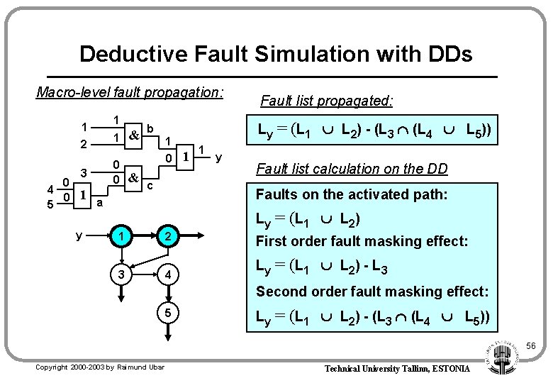
Deductive Fault Simulation with DDs Macro-level fault propagation: 1 1 2 0 4 0 5 1 0 0 3 1 y & & Ly b 1 0 c Fault list propagated: 1 1 y = (L 1 L 2) - (L 3 (L 4 L 5)) Fault list calculation on the DD Faults on the activated path: a Ly 1 2 3 4 = ( L 1 L 2) First order fault masking effect: Ly = ( L 1 L 2) - L 3 Second order fault masking effect: 5 Ly = (L 1 L 2) - (L 3 (L 4 L 5)) 56 Copyright 2000 -2003 by Raimund Ubar Technical University Tallinn, ESTONIA

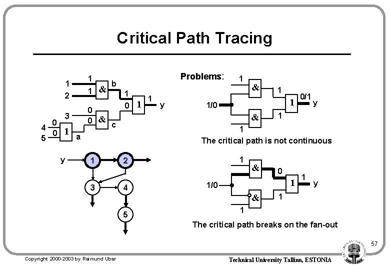
Critical Path Tracing 1 1 2 0 4 0 5 1 0 0 3 1 y & & Problems: b 1 0 1 1 1/0 0/1 y 1 1 The critical path is not continuous a 3 y & & c 1 1 1 2 4 & 1 1/0 & 5 0 1 y 1 1 The critical path breaks on the fan-out 57 Copyright 2000 -2003 by Raimund Ubar Technical University Tallinn, ESTONIA

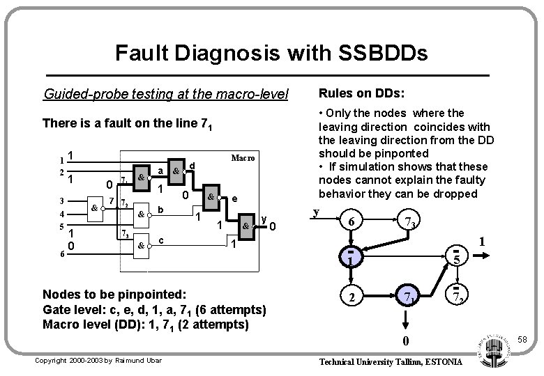
Fault Diagnosis with SSBDDs Guided-probe testing at the macro-level • Only the nodes where the leaving direction coincides with the leaving direction from the DD should be pinponted • If simulation shows that these nodes cannot explain the faulty behavior they can be dropped There is a fault on the line 71 1 2 1 1 3 & 4 5 6 0 1 0 71 & a 1 7 72 & 73 & b c Macro d & 0 & 1 e 1 & y y 0 6 73 1 1 Nodes to be pinpointed: Gate level: c, e, d, 1, a, 71 (6 attempts) Macro level (DD): 1, 71 (2 attempts) Copyright 2000 -2003 by Raimund Ubar Rules on DDs: 5 1 2 71 72 0 Technical University Tallinn, ESTONIA 58

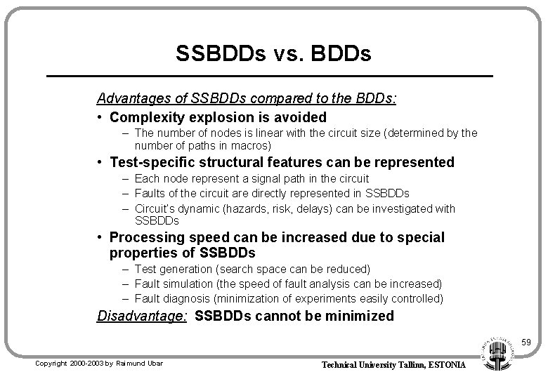
SSBDDs vs. BDDs Advantages of SSBDDs compared to the BDDs: • Complexity explosion is avoided – The number of nodes is linear with the circuit size (determined by the number of paths in macros) • Test-specific structural features can be represented – Each node represent a signal path in the circuit – Faults of the circuit are directly represented in SSBDDs – Circuit’s dynamic (hazards, risk, delays) can be investigated with SSBDDs • Processing speed can be increased due to special properties of SSBDDs – Test generation (search space can be reduced) – Fault simulation (the speed of fault analysis can be increased) – Fault diagnosis (minimization of experiments easily controlled) Disadvantage: SSBDDs cannot be minimized 59 Copyright 2000 -2003 by Raimund Ubar Technical University Tallinn, ESTONIA

SSBDDs vs. BDDs Increasing the Speed of Test Generation with SSBDDs Task: Activate a path to 1 Result: Tracing is forced in nodes 1, 9, 10 Output 0 Another trials possible from 2, 3, 4 Not needed Important property of SSBDD: N 4 1 9 11 1 A B 2 3 5 6 7 8 Breake search here Theorem: In SSBDD there exists always a path between the two successors A and B of N, either from A to B or from B to A 10 0 Copyright 2000 -2003 by Raimund Ubar Technical University Tallinn, ESTONIA 60

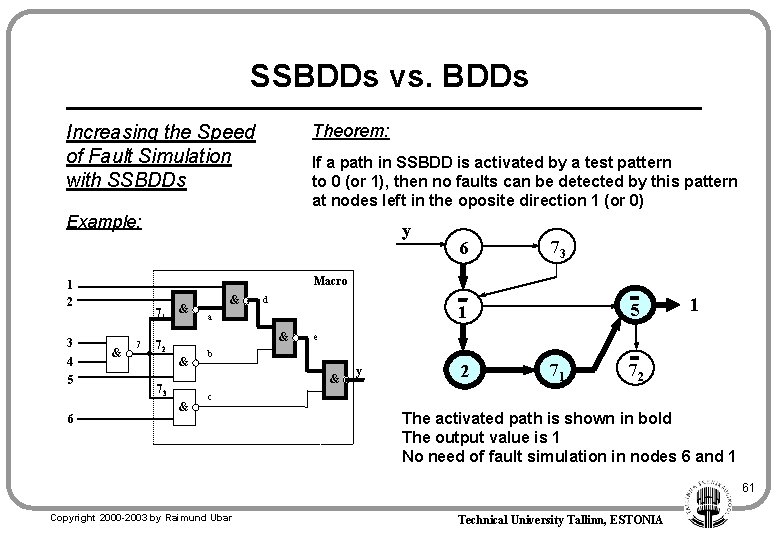
SSBDDs vs. BDDs Theorem: Increasing the Speed of Fault Simulation with SSBDDs If a path in SSBDD is activated by a test pattern to 0 (or 1), then no faults can be detected by this pattern at nodes left in the oposite direction 1 (or 0) Example: 4 5 6 6 73 Macro 1 2 3 y 71 & 7 & & d & 72 & & 1 e b & 73 5 1 a y 2 71 72 c The activated path is shown in bold The output value is 1 No need of fault simulation in nodes 6 and 1 61 Copyright 2000 -2003 by Raimund Ubar Technical University Tallinn, ESTONIA

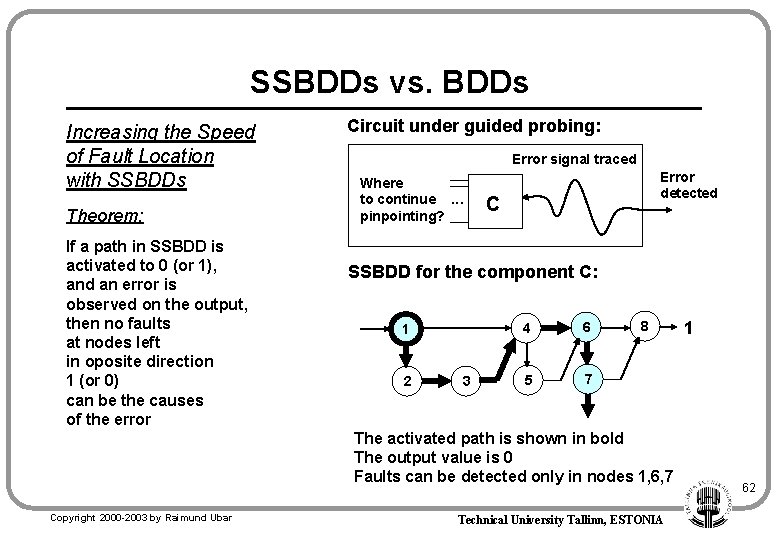
SSBDDs vs. BDDs Increasing the Speed of Fault Location with SSBDDs Theorem: If a path in SSBDD is activated to 0 (or 1), and an error is observed on the output, then no faults at nodes left in oposite direction 1 (or 0) can be the causes of the error Circuit under guided probing: Error signal traced Where to continue. . . pinpointing? Error detected C SSBDD for the component C: 1 2 3 4 6 5 7 8 The activated path is shown in bold The output value is 0 Faults can be detected only in nodes 1, 6, 7 Copyright 2000 -2003 by Raimund Ubar Technical University Tallinn, ESTONIA 1 62

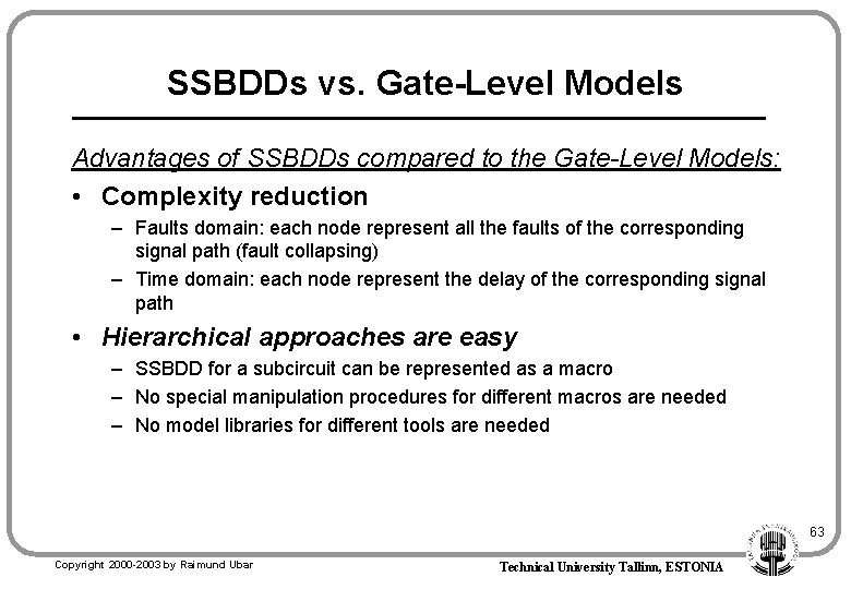
SSBDDs vs. Gate-Level Models Advantages of SSBDDs compared to the Gate-Level Models: • Complexity reduction – Faults domain: each node represent all the faults of the corresponding signal path (fault collapsing) – Time domain: each node represent the delay of the corresponding signal path • Hierarchical approaches are easy – SSBDD for a subcircuit can be represented as a macro – No special manipulation procedures for different macros are needed – No model libraries for different tools are needed 63 Copyright 2000 -2003 by Raimund Ubar Technical University Tallinn, ESTONIA

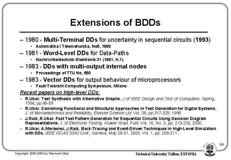
Extensions of BDDs – 1980 - Multi-Terminal DDs for uncertainty in sequential circuits (1993) • Automatika I Telemehanika, No 5, 1980 – 1981 - Word-Level DDs for Data-Paths • Nachrichtentechnik-Elektronik 31 (1981, H. 1) – 1983 - DDs with multi-output internal nodes • Proceedings of TTU No. 550 – 1983 - Vector DDs for output behaviour of microprocessors • Fault-Tolerant Computing Symposium, Milano Recent papers on high-level DDs: – R. Ubar. Test Synthesis with Alternative Graphs. J. of IEEE Design and Test of Computers. Spring, 1996, pp. 48 -59 – R. Ubar. Combining Functional and Structural Approaches in Test Generation for Digital Systems. J. of Microelectronics and Reliability, Elsevier Science Ltd. Vol. 38, pp. 317 -329, 1998 – J. Raik, R. Ubar. Fast Test Pattern Generation for Sequential Circuits Using Decision Diagram Representations. J. of Electronic Testing. Kluwer Acad. Publ. Vol. 16, No. 3, pp. 213 -226, 2000. – R. Ubar, A. Morawiec, J. Raik. Back-Tracing and Event-Driven Techniques in High-Level Simulation with DDs. IEEE ISCAS’ 2000 Conf. , Geneva, May 28 -31, 2000, Vol. 1, pp. 208 -211. 64 Copyright 2000 -2003 by Raimund Ubar Technical University Tallinn, ESTONIA

Outline • Introduction to Digital Test • How to improve test quality at increasing complexity of systems • High-level modelling and defect-orientation • BDDs and logic level testing • Hierarchical test generation – General concepts – Test generation for RT Level systems – Test generation for Microprocessors • Hierarchical fault simulation • Overview of tools developed at D&T Lab 65 Copyright 2000 -2003 by Raimund Ubar Technical University Tallinn, ESTONIA

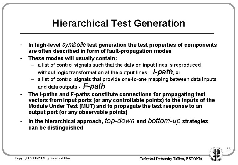
Hierarchical Test Generation • • In high-level symbolic test generation the test properties of components are often described in form of fault-propagation modes These modes will usually contain: – a list of control signals such that the data on input lines is reproduced without logic transformation at the output lines - I-path, or – a list of control signals that provide one-to-one mapping between data inputs and data outputs - F-path • The I-paths and F-paths constitute connections for propagating test vectors from input ports (or any controllable points) to the inputs of the Module Under Test (MUT) and to propagate the test response to an output port (or any observable points) • In the hierarchical approach, top-down and bottom-up strategies can be distinguished 66 Copyright 2000 -2003 by Raimund Ubar Technical University Tallinn, ESTONIA

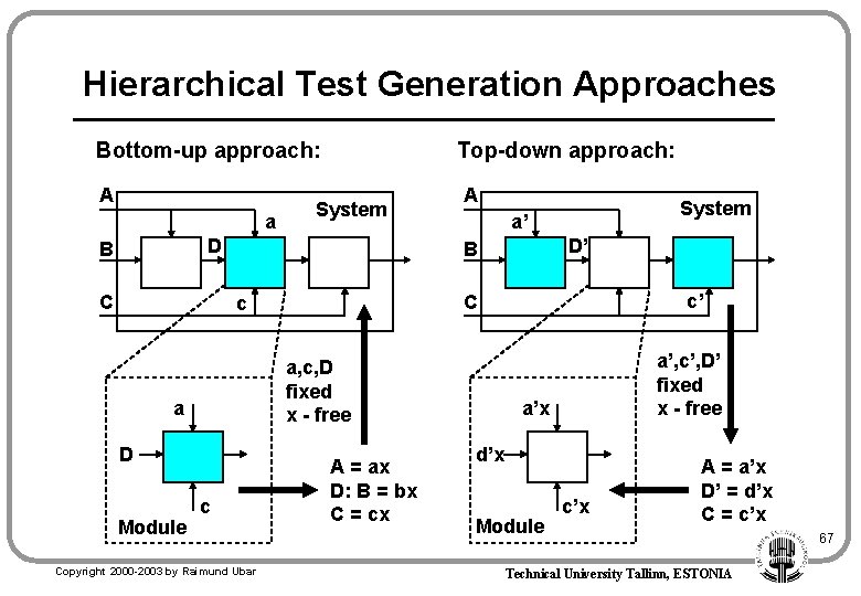
Hierarchical Test Generation Approaches Bottom-up approach: Top-down approach: A A a System D B C a, c, D fixed x - free D c Copyright 2000 -2003 by Raimund Ubar c’ C c Module D’ B a System a’ A = ax D: B = bx C = cx a’, c’, D’ fixed x - free a’x d’x Module c’x A = a’x D’ = d’x C = c’x Technical University Tallinn, ESTONIA 67

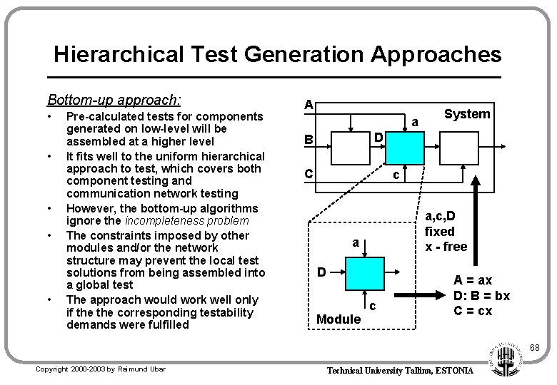
Hierarchical Test Generation Approaches Bottom-up approach: • • • Pre-calculated tests for components generated on low-level will be assembled at a higher level It fits well to the uniform hierarchical approach to test, which covers both component testing and communication network testing However, the bottom-up algorithms ignore the incompleteness problem The constraints imposed by other modules and/or the network structure may prevent the local test solutions from being assembled into a global test The approach would work well only if the corresponding testability demands were fulfilled A a System D B C c a, c, D fixed x - free a D Module c A = ax D: B = bx C = cx 68 Copyright 2000 -2003 by Raimund Ubar Technical University Tallinn, ESTONIA

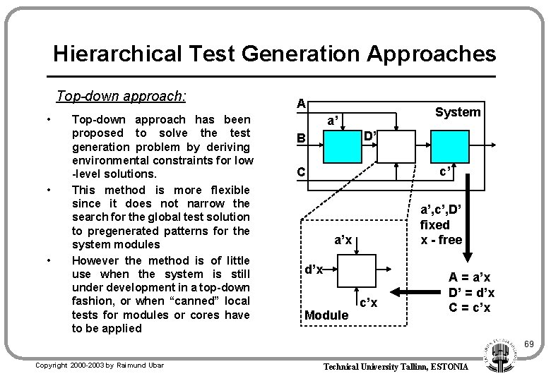
Hierarchical Test Generation Approaches Top-down approach: • • • Top-down approach has been proposed to solve the test generation problem by deriving environmental constraints for low -level solutions. This method is more flexible since it does not narrow the search for the global test solution to pregenerated patterns for the system modules However the method is of little use when the system is still under development in a top-down fashion, or when “canned” local tests for modules or cores have to be applied A System a’ D’ B c’ C a’, c’, D’ fixed x - free a’x d’x Module c’x A = a’x D’ = d’x C = c’x 69 Copyright 2000 -2003 by Raimund Ubar Technical University Tallinn, ESTONIA

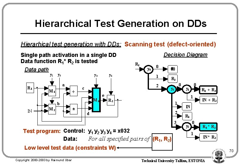
Hierarchical Test Generation on DDs Hierarhical test generation with DDs: Scanning test (defect-oriented) Single path activation in a single DD Data function R 1* R 2 is tested Data path R 1 y 2 y 3 a · M 1 + · M 2 * R 2 y 4 0 1 2 M 3 · y 4 c b · IN y 1 Decision Diagram e #0 R 2 0 y 3 0 y 1 R 1 + R 2 1 R 2 · 1 2 d 3 Test program: Control: y 1 y 2 y 3 y 4 = x 032 Data: For all specified pairs of (R 1, R 2) IN + R 2 IN R 1 y 2 0 1 R 1 * R 2 IN* R 2 Low level test data (constraints W) Copyright 2000 -2003 by Raimund Ubar 70 Technical University Tallinn, ESTONIA

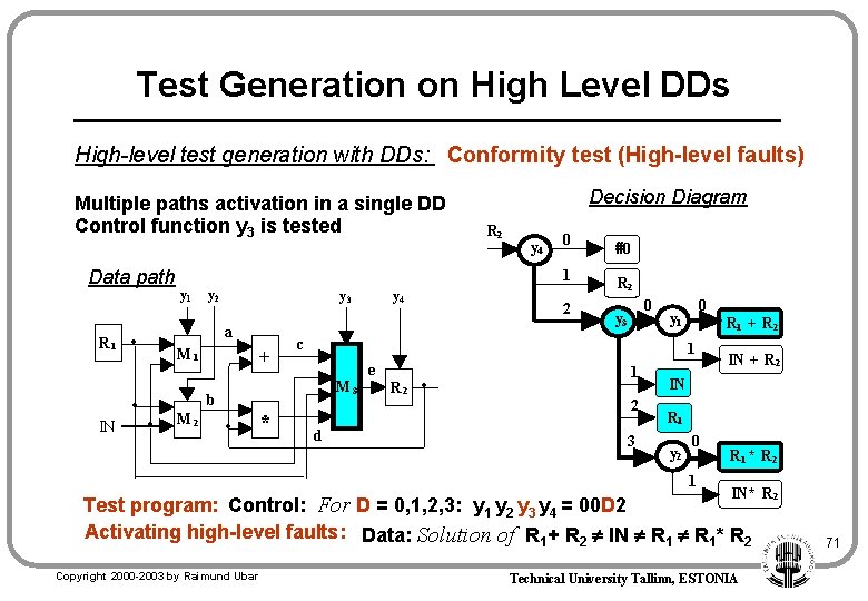
Test Generation on High Level DDs High-level test generation with DDs: Conformity test (High-level faults) Multiple paths activation in a single DD Control function y 3 is tested Data path R 1 IN y 1 y 2 y 3 M 1 + · y 4 0 M 2 * 2 R 2 0 y 3 0 y 1 R 1 + R 2 1 M 3 · y 4 #0 c b · R 2 1 a · Decision Diagram e R 2 · 1 2 d 3 IN + R 2 IN R 1 y 2 0 1 R 1 * R 2 IN* R 2 Test program: Control: For D = 0, 1, 2, 3: y 1 y 2 y 3 y 4 = 00 D 2 Activating high-level faults: Data: Solution of R 1+ R 2 IN R 1* R 2 Copyright 2000 -2003 by Raimund Ubar Technical University Tallinn, ESTONIA 71

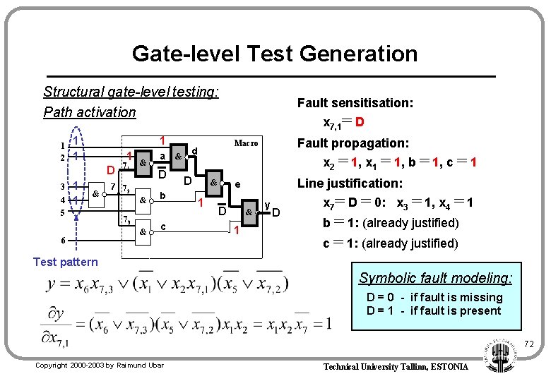
Gate-level Test Generation Structural gate-level testing: Path activation 1 2 1 1 D 3 4 1 1 & 5 6 71 & a D 7 72 & 73 & b c & Fault sensitisation: x 7, 1= D Fault propagation: Macro d x 2 = 1, x 1 = 1, b = 1, c = 1 D & 1 Line justification: e D & 1 y D x 7= D = 0: x 3 = 1, x 4 = 1 b = 1: (already justified) c = 1: (already justified) Test pattern Symbolic fault modeling: D = 0 - if fault is missing D = 1 - if fault is present 72 Copyright 2000 -2003 by Raimund Ubar Technical University Tallinn, ESTONIA

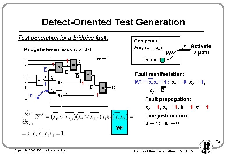
Defect-Oriented Test Generation Test generation for a bridging fault: Component F(x 1, x 2, …, xn) Bridge between leads 73 and 6 1 2 1 3 & 4 5 6 D 71 7 72 1 & D & 1 73 0 a & b c & Macro d & D 1 Wd a path Defect Fault manifestation: e D y Activate & y Wd = x 6 x 7= 1: x 6 = 0, x 7 = 1, D x 7 = D 1 Fault propagation: x 2 = 1, x 1 = 1, b = 1, c = 1 Line justification: Wd b = 1: x 5 = 0 73 Copyright 2000 -2003 by Raimund Ubar Technical University Tallinn, ESTONIA

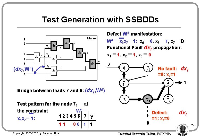
Test Generation with SSBDDs Macro 1 2 3 4 5 (dx 7, Wd) Defect Wd manifestation: 71 & 7 & & a x 1 = 1, x 2 = 1, x 5 = 0 e b & 73 & Wd = x 6 x 7= 1: x 6 = 0, x 7 = 1, x 7 = D Functional Fault dx 7 propagation: d & 72 6 & y c y 6 73 No fault: dx 7 =0: x 7=1 5 1 1 Bridge between leads 7 and 6: (dx 7, Wd) Test pattern for the node 71 the constraint x 6 x 7= 1: at 2 71 Wd = 123 4 5 6 7 y 11 Copyright 2000 -2003 by Raimund Ubar 00 1 1 0 72 Defect: =1: x 7=0 Technical University Tallinn, ESTONIA dx 7 74

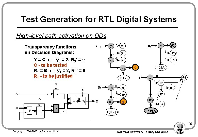
Test Generation for RTL Digital Systems High-level path activation on DDs Y, R 3 Transparency functions on Decision Diagrams: 1 2 Y = C y 3 = 2, R 3’ = 0 C - to be tested R 1 = B y 1 = 2, R 3’ = 0 R 1 - to be justified C R 1 B 1 R 2 F R 1 + * C s y 1 0 2 R 3 Y R’ 3 0 F(B, R’ 3 ) 0 y 2 R 2 1 R’ 3 2 R’ 2 0 C+R’ 2 y 3 y 1 0 #0 R’ 2 y 2 A 0 y 3 3 C R’ 2 A 2 R’ 2 C A 0 #0 0 R’ 1 1 1 #0 #1 R’ 1 B #0 R’ 1 0 1 A A* R’ 1 75 Copyright 2000 -2003 by Raimund Ubar Technical University Tallinn, ESTONIA

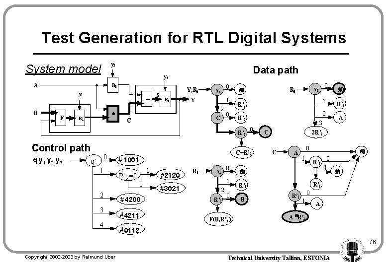
Test Generation for RTL Digital Systems y 2 System model A R 2 y 1 B F Data path y 3 + * R 1 s Y, R 3 0 y 3 1 Y 2 C C 0 #0 q y 1 y 2 y 3 0 q’ 1 2 3 4 2 R’ 2 2 0 C+R’ 2 # 1001 R’ 2 =0 1 R’ 3 R’ 2 Control path 1 0 # 4200 # 4211 #2120 ##3021 R 1 y 1 0 1 2 R’ 3 0 F(B, R’ 3 ) 0 y 2 R’ 2 A 2 R’ 2 C C A 0 #0 0 R’ 1 1 1 #0 #1 R’ 1 B 3 #0 R’ 1 0 1 A A *R’ 1 # 0112 76 Copyright 2000 -2003 by Raimund Ubar Technical University Tallinn, ESTONIA

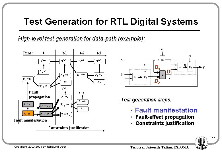
Test Generation for RTL Digital Systems High-level test generation for data-path (example): t Time: q’=4 t-2 t-3 q’=2 q’=1 q’=0 D 1 y =2 3 y R 3=D 2 R’ 2 = 0 =0 2 =0 D 2 q’=1 y =2 1 1 R’ 3 =0 R’ 1 = D 2 B =D A =D 1 D q’=2 Fault propagation C =D y =0 2 # 0 R’ A * R’ t-1 y =0 3 # 0 2 Fault manifestation Constraints justification Test generation steps: • Fault manifestation • Fault-effect propagation • Constraints justification 77 Copyright 2000 -2003 by Raimund Ubar Technical University Tallinn, ESTONIA

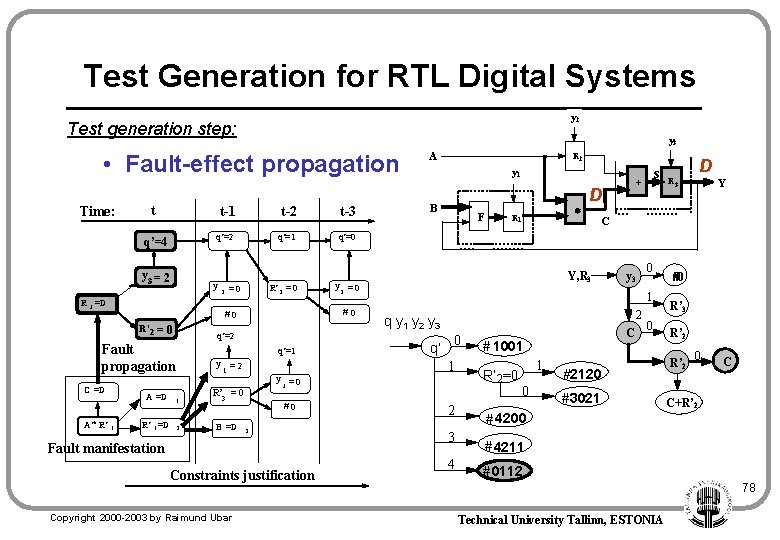
Test Generation for RTL Digital Systems y 2 Test generation step: y 3 • Fault-effect propagation Time: t q’=4 y 3 = 2 t-3 q’=2 q’=1 q’=0 y R 3 =D 2 R’ 2 = 0 =0 =0 q’=2 Fault propagation C =D A =D 1 R’ 1 =D q’=1 R’ 3 = 0 2 B =D B F # 0 2 Constraints justification * R 1 s + D 0 y 3 1 2 q y 1 y 2 y 3 q’ 0 2 3 4 C # 1001 R’ 2 =0 1 0 D R 3 Y C Y, R 3 y =0 3 Fault manifestation Copyright 2000 -2003 by Raimund Ubar y 1 1 y =2 1 1 R 2 y =0 2 # 0 R’ 2 A * R’ t-1 A 0 #2120 ##3021 #4200 #0 R’ 3 R’ 2 0 C C+R’ 2 # 4211 # 0112 78 Technical University Tallinn, ESTONIA

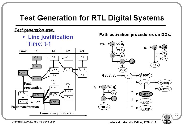
Test Generation for RTL Digital Systems Test generation step: Path activation procedures on DDs: • Line justification Time: t-1 t Time: t-1 q’=4 t-2 q’=1 y 3 00 Y, R 3 1 t-3 2 C q’=0 0 #0 R’ 3 y R 3 =D =0 R’ 2 = 0 =0 A =D 1 y =0 2 C 3 R’ 2 A C+R’ 2 # 0 q y 1 y 2 y 3 R’ 1 =D q’=1 y =2 1 1 R’ 3 =0 2 B =D 0 q’ 1 q’=2 Fault propagation A * R’ 2 # 0 C =D 2 #0 2 R’ 2 y =2 3 2 1 R’ 2 R’ y 2 0 R 2 R 1 0 y 1 y =0 3 # 0 1 2 R’ 3 0 #0 R’ 1 2 B 3 2 Fault manifestation F(B, R’ 3 ) 4 # 1001 R’ 2 =0 1 0 ##3021 # 4200 # 4211 # 0112 Constraints justification Copyright 2000 -2003 by Raimund Ubar #2120 79 Technical University Tallinn, ESTONIA

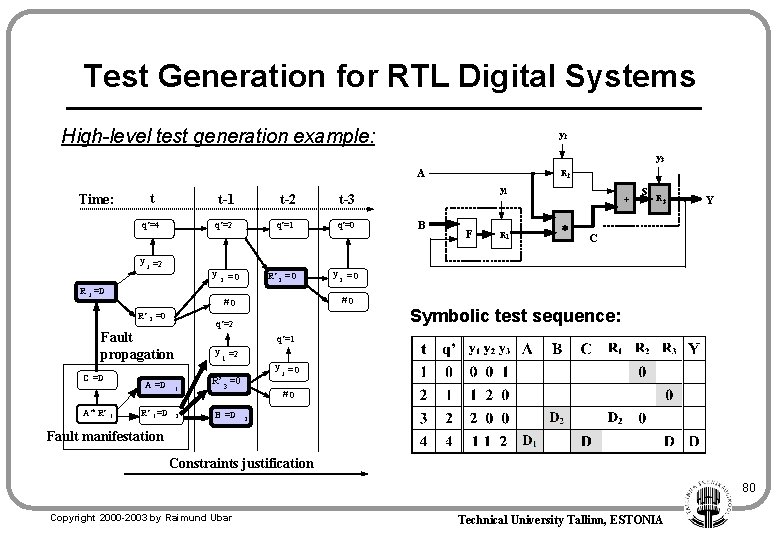
Test Generation for RTL Digital Systems High-level test generation example: y 2 y 3 A t t-1 t-2 t-3 q’=4 q’=2 q’=1 q’=0 Time: y =2 3 y R 3 =D R’ 2 = 0 =0 2 =0 C =D 1 B F R 1 + * s R 3 Y C y =0 2 Symbolic test sequence: q’=2 Fault propagation y 1 # 0 R’ A * R’ 2 R 2 q’=1 y =2 1 A =D 1 R’ 3 =0 R’ 1 =D 2 B =D y =0 3 # 0 2 Fault manifestation Constraints justification 80 Copyright 2000 -2003 by Raimund Ubar Technical University Tallinn, ESTONIA

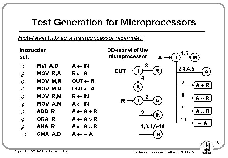
Test Generation for Microprocessors High-Level DDs for a microprocessor (example): DD-model of the microprocessor: Instruction set: I 1 : I 2 : I 3 : I 4 : I 5 : I 6 : I 7 : I 8 : I 9 : I 10: MVI A, D MOV R, A MOV M, R MOV M, A MOV R, M MOV A, M ADD R ORA R ANA R CMA A, D A IN R A OUT R OUT A R IN A A+R A A OUT 3 I A R 4 2 I 5 1, 6 IN 2, 3, 4, 5 7 A R I A 8 9 IN 10 1, 3, 4, 6 -10 A A+R A R A R 81 Copyright 2000 -2003 by Raimund Ubar Technical University Tallinn, ESTONIA

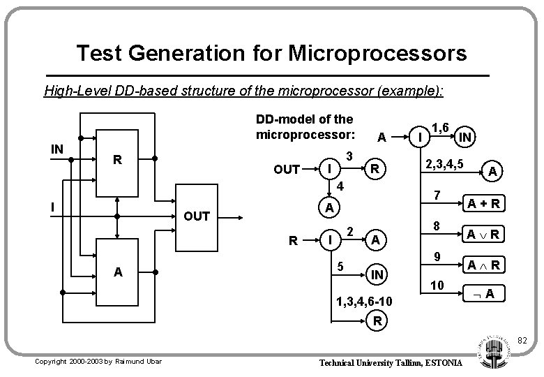
Test Generation for Microprocessors High-Level DD-based structure of the microprocessor (example): DD-model of the microprocessor: IN R OUT 3 I A R 4 I R A 2 I 5 1, 6 IN 2, 3, 4, 5 7 A OUT I A 8 9 IN 10 1, 3, 4, 6 -10 A A+R A R A R 82 Copyright 2000 -2003 by Raimund Ubar Technical University Tallinn, ESTONIA

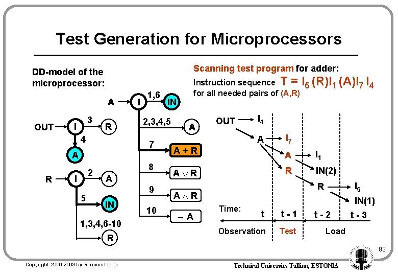
Test Generation for Microprocessors Scanning test program for adder: DD-model of the microprocessor: A OUT 3 I R 4 I 1, 6 A R 2 I 5 8 A 9 IN 1, 3, 4, 6 -10 R IN 2, 3, 4, 5 7 10 Instruction sequence T = I 5 (R)I 1 (A)I 7 I 4 for all needed pairs of (A, R) A OUT I 4 A I 7 A+R A I 1 A R R IN(2) A R A I 5 R Time: IN(1) t t-1 Observation Test t-2 t-3 Load 83 Copyright 2000 -2003 by Raimund Ubar Technical University Tallinn, ESTONIA

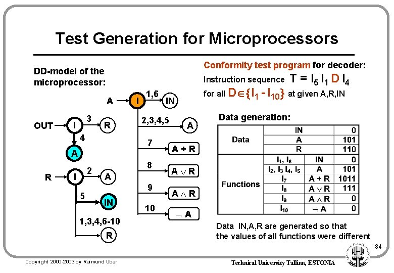
Test Generation for Microprocessors Conformity test program for decoder: DD-model of the microprocessor: Instruction sequence A OUT 3 I R 4 I 1, 6 7 A R 2 I 5 8 A 9 IN 1, 3, 4, 6 -10 R 10 for all D I 1 - I 10 at given A, R, IN IN 2, 3, 4, 5 T = I 5 I 1 D I 4 A Data generation: A+R A R A Data IN, A, R are generated so that the values of all functions were different 84 Copyright 2000 -2003 by Raimund Ubar Technical University Tallinn, ESTONIA

Outline • Introduction to Digital Test • How to improve test quality at increasing complexity of systems • High-level modelling and defect-orientation • BDDs and logic level testing • Hierarchical test generation – General concepts – Test generation for RT Level systems – Test generation for Microprocessors • Hierarchical fault simulation • Overview of tools developed at D&T Lab 85 Copyright 2000 -2003 by Raimund Ubar Technical University Tallinn, ESTONIA

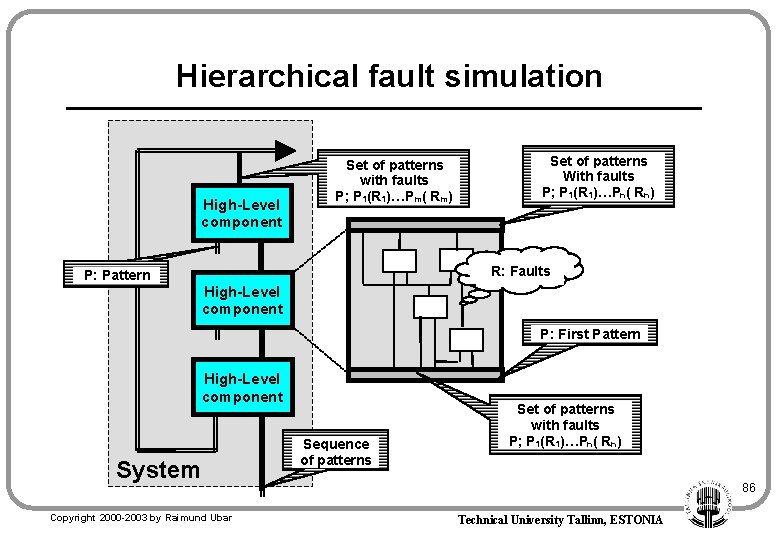
Hierarchical fault simulation High-Level component P: Pattern Set of patterns with faults P; P 1(R 1)…Pm( Rm) Set of patterns With faults P; P 1(R 1)…Pn( Rn) R: Faults High-Level component P: First Pattern High-Level component System Copyright 2000 -2003 by Raimund Ubar Sequence of patterns Set of patterns with faults P; P 1(R 1)…Pn( Rn) 86 Technical University Tallinn, ESTONIA

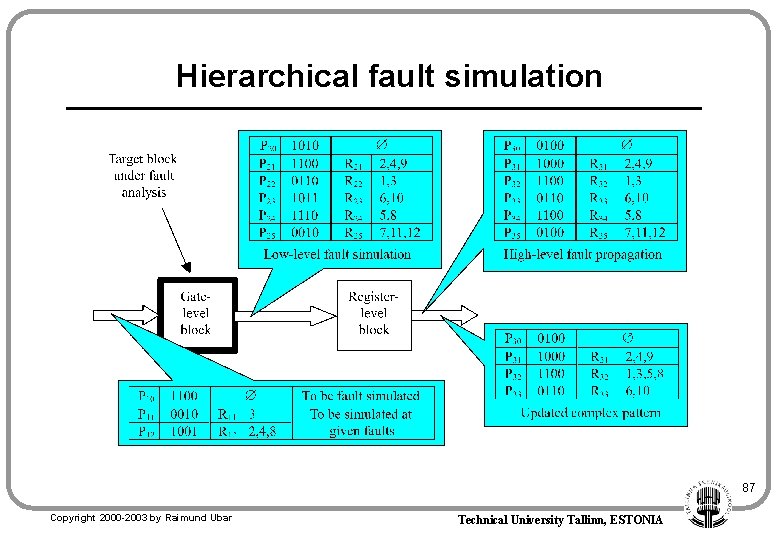
Hierarchical fault simulation 87 Copyright 2000 -2003 by Raimund Ubar Technical University Tallinn, ESTONIA

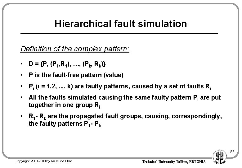
Hierarchical fault simulation Definition of the complex pattern: • D = {P, (P 1, R 1), …, (Pk, Rk)} • P is the fault-free pattern (value) • Pi (i = 1, 2, . . . , k) are faulty patterns, caused by a set of faults Ri • All the faults simulated causing the same faulty pattern Pi are put together in one group Ri • R 1 - Rk are the propagated fault groups, causing, correspondingly, the faulty patterns P 1 - Pk 88 Copyright 2000 -2003 by Raimund Ubar Technical University Tallinn, ESTONIA

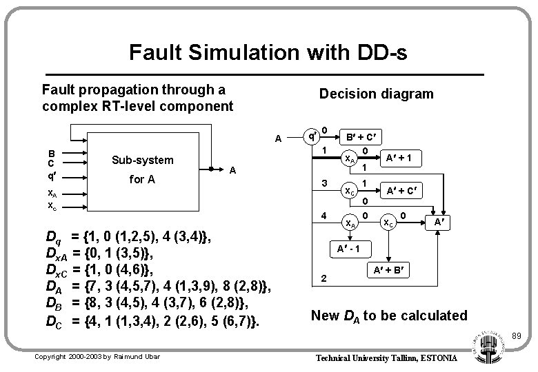
Fault Simulation with DD-s Fault propagation through a complex RT-level component Decision diagram A B C q Sub-system for A q 0 1 A xc Dq = {1, 0 (1, 2, 5), 4 (3, 4)}, Dx. A = {0, 1 (3, 5)}, Dx. C = {1, 0 (4, 6)}, DA = {7, 3 (4, 5, 7), 4 (1, 3, 9), 8 (2, 8)}, DB = {8, 3 (4, 5), 4 (3, 7), 6 (2, 8)}, DC = {4, 1 (1, 3, 4), 2 (2, 6), 5 (6, 7)}. 3 4 B + C 0 x. A 1 x. C x. A 1 0 0 A + 1 A + C x. C 0 A A - 1 2 A + B New DA to be calculated 89 Copyright 2000 -2003 by Raimund Ubar Technical University Tallinn, ESTONIA

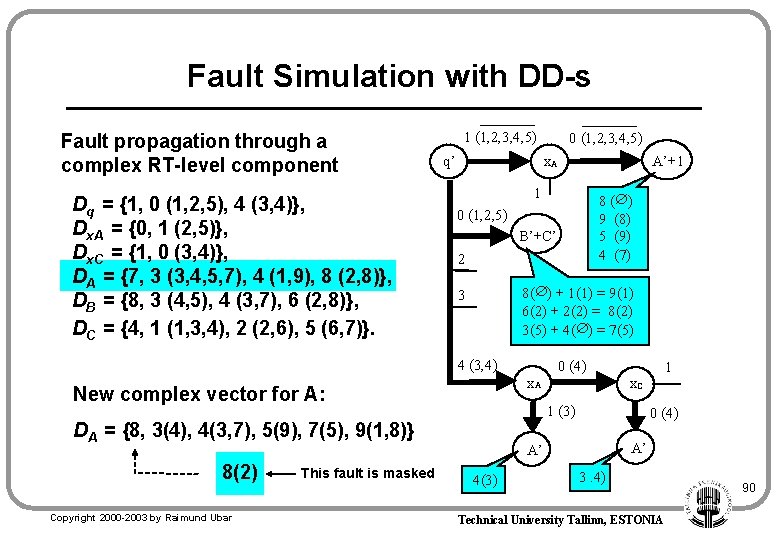
Fault Simulation with DD-s Fault propagation through a complex RT-level component Dq = {1, 0 (1, 2, 5), 4 (3, 4)}, Dx. A = {0, 1 (2, 5)}, Dx. C = {1, 0 (3, 4)}, DA = {7, 3 (3, 4, 5, 7), 4 (1, 9), 8 (2, 8)}, DB = {8, 3 (4, 5), 4 (3, 7), 6 (2, 8)}, DC = {4, 1 (1, 3, 4), 2 (2, 6), 5 (6, 7)}. 1 (1, 2, 3, 4, 5) q’ x. A B’+C’ 2 8(Æ) + 1(1) = 9(1) 6(2) + 2(2) = 8(2) 3(5) + 4(Æ) = 7(5) 3 x. A 0 (4) A’ A’ 4(3) 1 x. C 1 (3) DA = {8, 3(4), 4(3, 7), 5(9), 7(5), 9(1, 8)} Copyright 2000 -2003 by Raimund Ubar 8 (Æ ) 9 (8) 5 (9) 4 (7) 0 (1, 2, 5) New complex vector for A: This fault is masked A’+1 1 4 (3, 4) 8(2) 0 (1, 2, 3, 4, 5) 3. 4) Technical University Tallinn, ESTONIA 90

Outline • Introduction to Digital Test • How to improve test quality at increasing complexity of systems • High-level modelling and defect-orientation • BDDs and logic level testing • Hierarchical test generation – General concepts – Test generation for RT Level systems – Test generation for Microprocessors • Overview of tools developed at D&T Lab 91 Copyright 2000 -2003 by Raimund Ubar Technical University Tallinn, ESTONIA

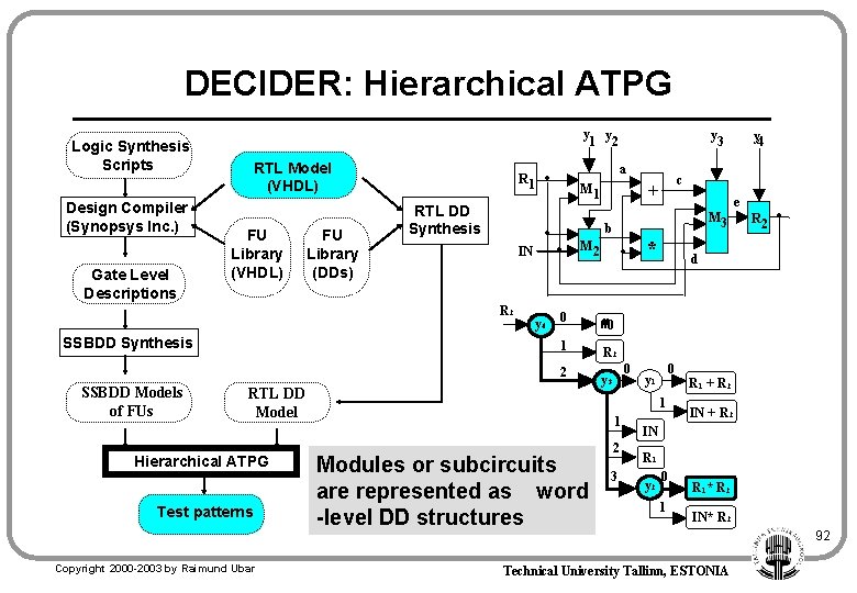
DECIDER: Hierarchical ATPG Logic Synthesis Scripts Design Compiler (Synopsys Inc. ) Gate Level Descriptions y 1 y 2 RTL Model (VHDL) FU Library (DDs) y 4 M 2 #0 1 R 2 RTL DD Model Hierarchical ATPG Test patterns Copyright 2000 -2003 by Raimund Ubar · 0 2 SSBDD Models of FUs M 3 b · IN 0 y 3 * Modules or subcircuits are represented as word -level DD structures 2 3 e R 2 · d 0 y 1 1 1 y 4 c + M 1 · R 2 SSBDD Synthesis a R 1 · RTL DD Synthesis y 3 R 1 + R 2 IN R 1 y 2 0 1 R 1* R 2 IN* R 2 Technical University Tallinn, ESTONIA 92

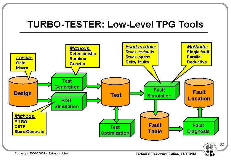
TURBO-TESTER: Low-Level TPG Tools Methods: Deterministic Random Genetic Levels: Gate Macro Fault models: Methods: Stuck-at-faults Stuck-opens Delay faults Single fault Parallel Deductive Test Generation Design Test BIST Simulation Fault Location Fault Table Fault Diagnosis Methods: BILBO CSTP Store/Generate Test Optimization 93 Copyright 2000 -2003 by Raimund Ubar Technical University Tallinn, ESTONIA

Conclusions • Physical defects can be formally mapped to the logical level by Boolean differential calculus • Functional fault model is a universal means for mapping test results from lower levels to higher levels, giving a formal basis for hierarchical approaches to test generation and fault simulation • Decision diagrams is a suitable tool which can be used successfully both, on the logic level, and also on higher register transfer or behavioral levels 94 Copyright 2000 -2003 by Raimund Ubar Technical University Tallinn, ESTONIA

References 1. 2. 3. 4. 5. 6. 7. 8. S. Mourad, Y. Zorian. Principles of Testing Electronic Systems. J. Wiley & Sons, Inc. New York, 2000, 420 p. M. L. Bushnell, V. D. Agrawal. Essentials of Electronic testing. Kluwer Acad. Publishers, 2000, 690 p. M. Abramovici et. al. Digital Systems Testing & Testable Designs. Computer Science Press, 1995, 653 p. S. Minato. Binary Decision Diagrams and Applications for VLSI CAD. Kluwer Academic Publishers, 1996, 141 p. R. Ubar. Test Synthesis with Alternative Graphs. IEEE Design and Test of Computers. Spring, 1996, pp. 48 -59. J. Raik, R. Ubar. Fast Test Pattern Generation for Sequential Circuits Using Decision Diagram Representations. JETTA: Theory and Applications. Kluwer Academic Publishers. Vol. 16, No. 3, pp. 213 -226, 2000. R. Ubar, W. Kuzmicz, W. Pleskacz, J. Raik. Defect-Oriented Fault Simulation and Test Generation in Digital Circuits. ISQED’ 02, San Jose, California, March 26 -28, 2001, pp. 365 -371. T. Cibáková, M. Fischerová, E. Gramatová, W. Kuzmicz, W. Pleskacz, J. Raik, R. Ubar. Hierarchical Test Generation with Real Defects Coverage. Pergamon Press. J. of Microelectronics Reliability, Vol. 42, 2002, pp. 1141 -114. 95 Copyright 2000 -2003 by Raimund Ubar Technical University Tallinn, ESTONIA

References • European Projects: – EEMCN, FUTEG, ATSEC, SYTIC, VILAB, REASON, e. VIKINGS II • Special thanks to: – EU project IST-2000 -30193 REASON – Cooperation partners: IISAS Bratislava, TU Warsaw – Colleagues: J. Raik, A. Jutman, E. Ivask, E. Orasson a. o. (TU Tallinn) • Contact data: – – – Tallinn Technical University Computer Engineering Department Address: Raja tee 15, 12618 Tallinn, Estonia Tel. : +372 620 2252, Fax: +372 620 2253 E-mail: raiub@pld. ttu. ee www. ttu. ee/ˇraiub/ 96 Copyright 2000 -2003 by Raimund Ubar Technical University Tallinn, ESTONIA