
Keyboard Controller Design By Tamas Kasza A Project
Keyboard Controller Design By Tamas Kasza A Project Proposal for Digital System Design 2 (ECE 5572) Summer 2003 1
Design Goals n n n Attach a keyboard to the I/O device through PS/2 type of port; Design a logic which can detect and display a pushed character on the LCD display of the I/O device; Use VHDL during the development process. 2
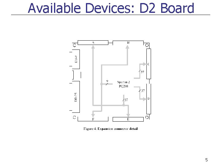
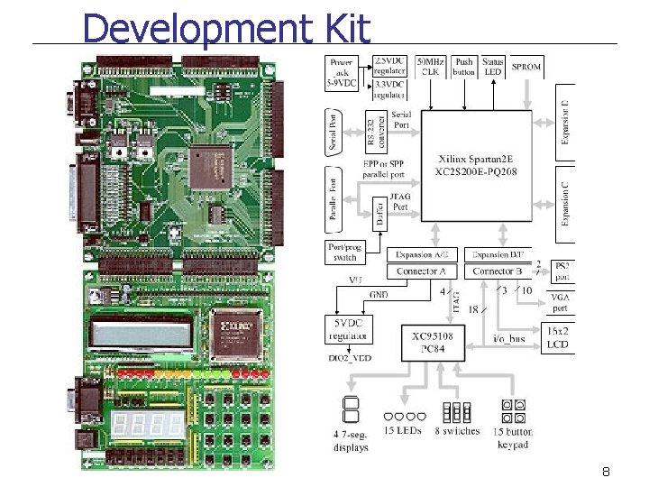
Available Devices: D 2 Board Digilab 2 (D 2) FPGA-based development board with a 200 K-gate Xilinx Spartan 2 XC 2 S 200 FPGA in a PQ 208 package that provides 143 user I/Os Attached parallel port cable for communication with the PC Attached AC/DC adaptor: 110 V (AC) 6 V (DC) 3
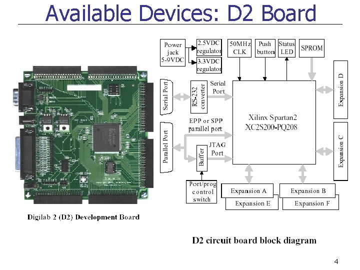
Available Devices: D 2 Board 4
Available Devices: D 2 Board 5
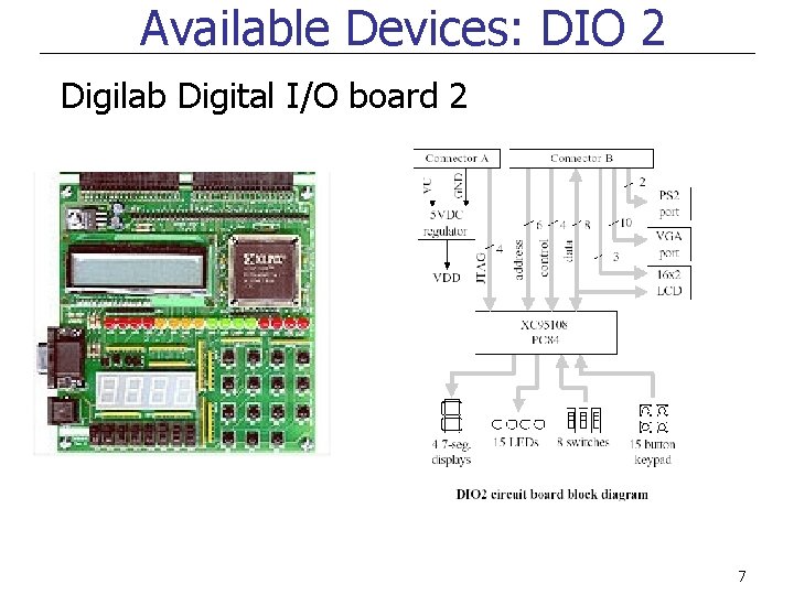
Available Devices: DIO 2 Digilab Digital I/O board 2 n 16 x 2 character LCD Four seven segment displays 16 LEDs in three colors 8 switches 15 pushbutton keypad 8 -bit VGA port n PS/2 port n n n 6
Available Devices: DIO 2 Digilab Digital I/O board 2 7
Development Kit 8
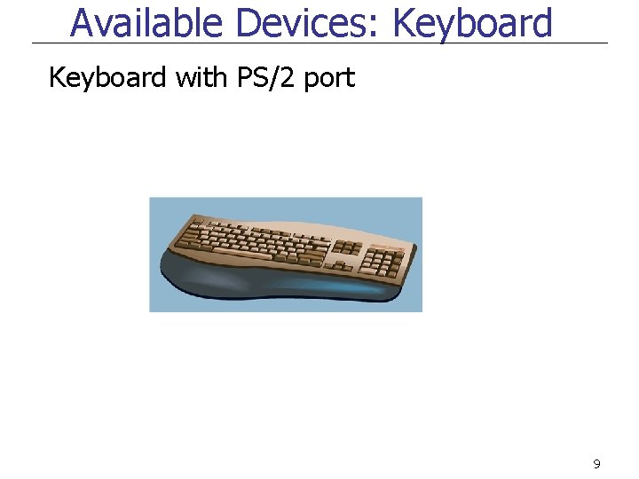
Available Devices: Keyboard with PS/2 port 9
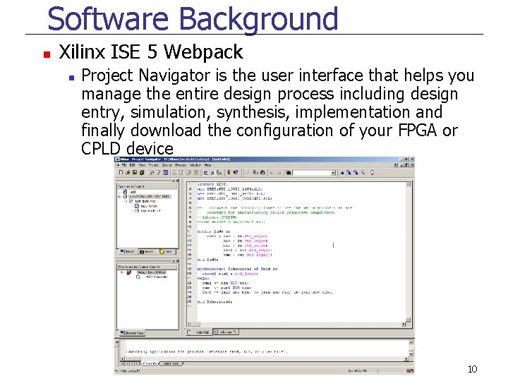
Software Background n Xilinx ISE 5 Webpack n Project Navigator is the user interface that helps you manage the entire design process including design entry, simulation, synthesis, implementation and finally download the configuration of your FPGA or CPLD device 10
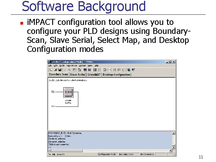
Software Background n i. MPACT configuration tool allows you to configure your PLD designs using Boundary. Scan, Slave Serial, Select Map, and Desktop Configuration modes 11
PS/2 Interface n n The DIO II Board receives two signals from the PS/2 interface: a clock signal and a serial data stream that is synchronized with the falling edges on the clock signal. Connection identification: # PS/2 KEYBOARD CONNECTIONS NET KB_DATA LOC=P 69; NET KB_CLK LOC=P 68; 12
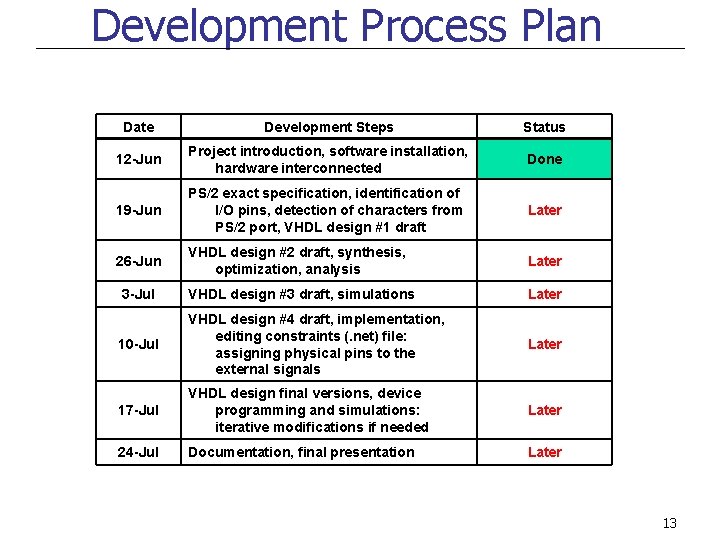
Development Process Plan Date Development Steps Status 12 -Jun Project introduction, software installation, hardware interconnected Done 19 -Jun PS/2 exact specification, identification of I/O pins, detection of characters from PS/2 port, VHDL design #1 draft Later 26 -Jun VHDL design #2 draft, synthesis, optimization, analysis Later 3 -Jul VHDL design #3 draft, simulations Later 10 -Jul VHDL design #4 draft, implementation, editing constraints (. net) file: assigning physical pins to the external signals Later 17 -Jul VHDL design final versions, device programming and simulations: iterative modifications if needed Later 24 -Jul Documentation, final presentation Later 13

Thank You for Your Attention! 14
- Slides: 14