July 2019 Mobile GPU approaches to power efficiency
July 2019 Mobile GPU approaches to power efficiency Andrew Gruber VP, Technology Qualcomm Technologies, Inc.
Overview • What is the typical mobile environment? • Rendering algorithm differences with desktop • Performance and perf/watt comparison with desktop • Physical design and power management 2
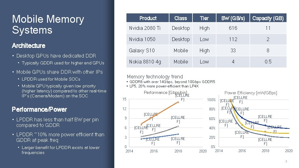
Mobile Memory Systems Product Architecture • Desktop GPUs have dedicated DDR • Typically GDDR used for higher end GPUs • Mobile GPUs share DDR with other IPs Performance/Power • LPDDR has less than half BW per pin compared to GDDR • LPDDR ~10% more power efficient than GDDR at peak freq • Larger benefit for LPDDR exists at lower frequencies Tier BW (GB/s) Capacity (GB) Nvidia 2080 Ti Desktop High 616 11 Nvidia 1050 Desktop Low 112 2 Galaxy S 10 Mobile High 33 8 Nokia 8810 4 g Mobile Low 4 0. 5 Memory technology trend • LPDDR used for Mobile SOCs • Mobile GPU typically given low priority (higher latency) compared to other real-time IP’s (Camera/Modem) on the SOC Class • GDDR 6 with over 14 Gbps, beyond 10 Gbps GDDR 5 • LP 5, 20% more power-efficient than LP 4 X Performance [Gbps/pin] Power Efficiency [m. W/GBps] [CELLRE F] 15 100% 12 9 6 3 0 2014 80% [CELLRE F] F] [CELLRE 40% F] [CELLRE F] 60% [CELLRE F] 20% 2016 2018 [CELLRE F] F] [CELLRE F] F] 2020 0% 2014 F] 2016 [CELLRE F] 2018 2020 3
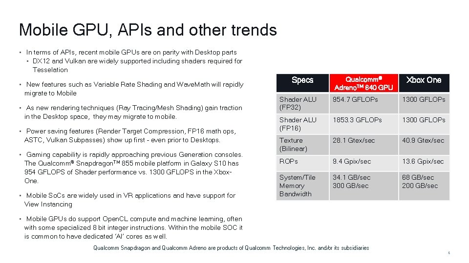
Mobile GPU, APIs and other trends • In terms of APIs, recent mobile GPUs are on parity with Desktop parts • DX 12 and Vulkan are widely supported including shaders required for Tesselation • New features such as Variable Rate Shading and Wave. Math will rapidly migrate to Mobile • As new rendering techniques (Ray Tracing/Mesh Shading) gain traction in the Desktop space, they may migrate to mobile. • Power saving features (Render Target Compression, FP 16 math ops, ASTC, Vulkan Subpasses) show up first – even prior to Desktops. • Gaming capability is rapidly approaching previous Generation consoles. The Qualcomm® Snapdragon. TM 855 mobile platform in Galaxy S 10 has 954 GFLOPS of Shader performance vs. 1300 GFLOPS in the Xbox. One. • Mobile So. Cs are widely used in VR applications and have support for View Instancing Specs Qualcomm® Adreno. TM 640 GPU Xbox One Shader ALU (FP 32) 954. 7 GFLOPs 1300 GFLOPs Shader ALU (FP 16) 1853. 3 GFLOPs 1300 GFLOPs Texture (Bilinear) 28. 1 Gtex/sec 40. 9 Gtex/sec ROPs 9. 4 Gpix/sec 13. 6 Gpix/sec System/Tile Memory Bandwidth 34. 1 GB/sec 300 GB/sec 68 GB/sec 200 GB/sec • Mobile GPUs do support Open. CL compute and machine learning, often with some specialized 8 bit integer instructions. Within the mobile SOC it is common to have dedicated ‘AI’ cores as well. Qualcomm Snapdragon and Qualcomm Adreno are products of Qualcomm Technologies, Inc. and/or its subsidiaries 4
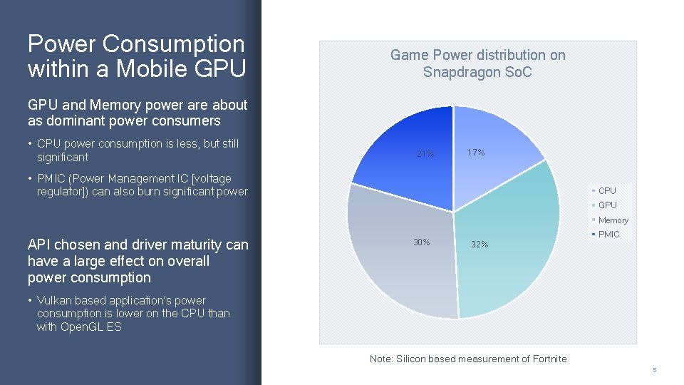
Power Consumption within a Mobile GPU Game Power distribution on Snapdragon So. C GPU and Memory power are about as dominant power consumers • CPU power consumption is less, but still significant 21% 17% • PMIC (Power Management IC [voltage regulator]) can also burn significant power CPU GPU Memory API chosen and driver maturity can have a large effect on overall power consumption 30% PMIC 32% • Vulkan based application’s power consumption is lower on the CPU than with Open. GL ES Note: Silicon based measurement of Fortnite 5
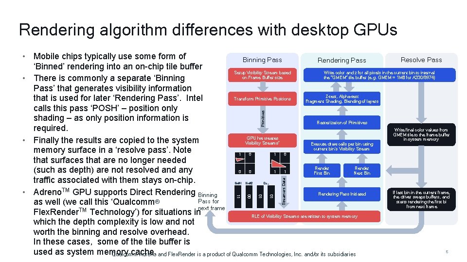
Rendering algorithm differences with desktop GPUs 11 00 Etc… 01 Bin#2 01 Bin#1 Streamers Data Primitives • Mobile chips typically use some form of Binning Pass Resolve Pass Rendering Pass ‘Binned’ rendering into an on-chip tile buffer Setup Visibility Stream based Write color and z for all pixels in the current bin to internal on Frame Buffer size the “GMEM” tile buffer (e. g. GMEM = 1 MB for A 330/8974) • There is commonly a separate ‘Binning Pass’ that generates visibility information Z-test, Alpha-test Transform Primitive Positions that is used for later ‘Rendering Pass’. Intel Fragment Shading, Blending of layers calls this pass ‘POSH’ – position only shading – as only position information is Rasterization of Primitives required. Write final color values from GMEM tile to the frame buffer GPU hw creates in system memory • Finally the results are copied to the system Visibility Streams* Execute draw calls per bin using current bin’s Visibility Stream memory surface in a ‘resolve pass’. Note 1 0 that surfaces that are no longer needed Render (such as depth) are not resolved any 0 0 1 1 First Bin Next Bin traffic associated with them stays on-chip. If last bin in the current frame, • Adreno. TM GPU supports Direct Rendering Binning Rendering Pass Initiated the driver swaps buffers, and starts rendering the first bi Pass for as well (we call this ‘Qualcomm® from next frame Flex. Render. TM Technology’) for situations in RLE of Visibility Streams are written to system memory which the depth complexity is low and not worth the binning and resolve overhead. In these cases, some of the tile buffer is 6 used as system memory cache. Qualcomm Adreno and Flex. Render is a product of Qualcomm Technologies, Inc. and/or its subsidiaries
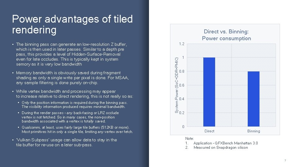
Power advantages of tiled rendering • Memory bandwidth is obviously saved during fragment shading as only a single write per pixel is done. For MSAA, any sample filtering is done purely on-chip. • While vertex bandwidth and processing may appear to increase relative to direct rendering, this is not really so as: • Only the position information is required during the binning pass. The visibility information produced requires minimal bandwidth. • During the render passes – any back-facing or LRZ occlude vertex is not fetched. So in many cases, the non-position bandwidth associated with a vertex is totally saved. • Qualcomm, at least, uses fairly large tile buffers (512 KB or more). Most primitives hit in only a single tile, limiting any vertex over fetch. • ‘Vulkan Subpass’ usage can allow data to stay in the tile buffer for re-use on a later sub-pass. 1. 2 System Power (So. C+DDR+PMIC) • The binning pass can generate an low-resolution Z buffer, which is then used in later passes. Similar to a depth pre pass, this provides a level of Hidden-Surface-Removal even for late occludes. This is typically kept in system semory as it is very low bandwidth Direct vs. Binning: Power consumption 1 0. 8 0. 6 0. 4 0. 2 0 Direct Binning Note: 1. Application – GFXBench Manhattan 3. 0 2. Measured on Snapdragon silicon 7
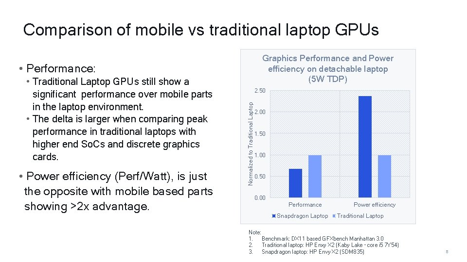
Comparison of mobile vs traditional laptop GPUs Graphics Performance and Power efficiency on detachable laptop (5 W TDP) • Performance: • Power efficiency (Perf/Watt), is just the opposite with mobile based parts showing >2 x advantage. 2. 50 Normalized to Traditional Laptop • Traditional Laptop GPUs still show a significant performance over mobile parts in the laptop environment. • The delta is larger when comparing peak performance in traditional laptops with higher end So. Cs and discrete graphics cards. 2. 00 1. 50 1. 00 0. 50 0. 00 Performance Snapdragon Laptop Power efficiency Traditional Laptop Note: 1. Benchmark: DX 11 based GFXbench Manhattan 3. 0 2. Traditional laptop: HP Enxy X 2 (Kaby Lake – core i 5 7 Y 54) 3. Snapdragon laptop: HP Envy X 2 (SDM 835) 8
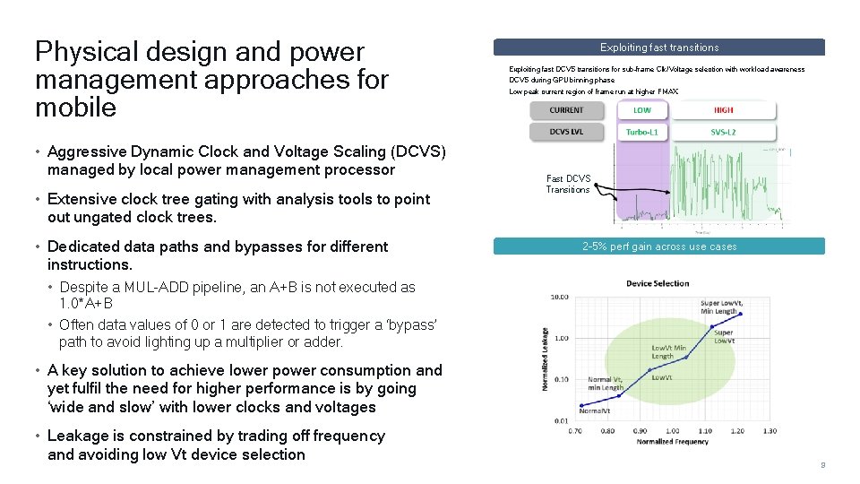
Physical design and power management approaches for mobile • Aggressive Dynamic Clock and Voltage Scaling (DCVS) managed by local power management processor • Extensive clock tree gating with analysis tools to point out ungated clock trees. • Dedicated data paths and bypasses for different instructions. Exploiting fast transitions Exploiting fast DCVS transitions for sub-frame Clk/Voltage selection with workload awareness DCVS during GPU binning phase Low peak current region of frame run at higher FMAX Fast DCVS Transitions 2 -5% perf gain across use cases Ack: Edwin Jose • Despite a MUL-ADD pipeline, an A+B is not executed as 1. 0*A+B • Often data values of 0 or 1 are detected to trigger a ‘bypass’ path to avoid lighting up a multiplier or adder. • A key solution to achieve lower power consumption and yet fulfil the need for higher performance is by going ‘wide and slow’ with lower clocks and voltages • Leakage is constrained by trading off frequency and avoiding low Vt device selection 9
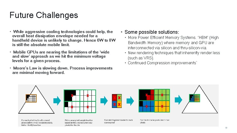
Future Challenges • While aggressive cooling technologies could help, the • Some possible solutions: overall heat dissipation envelope needed for a • More Power Efficient Memory Systems. ‘HBM’ (High handheld device is unlikely to change. Hence 6 W to 8 W Bandwidth Memory) where memory and GPU are is still the absolute mobile limit. • Mobile GPUs are nearing the limitations of the ‘wide and slow’ approach as we hit the minimum voltage levels for a given process. interconnected via silicon and thru-silicon-via. • New rendering techniques that inherently render less (such as VRS). • Continued Compression improvements` • Moore’s Law is slowing down. Process improvements are minimal moving forward. 10
Thank you Follow us on: For more information, visit us at: www. qualcomm. com & www. qualcomm. com/blog Nothing in these materials is an offer to sell any of the components or devices referenced herein. © 2018 -2019 Qualcomm Technologies, Inc. and/or its affiliated companies. All Rights Reserved. Qualcomm, Snapdragon and Adreno are trademarks of Qualcomm Incorporated, registered in the United States and other countries. Other products and brand names may be trademarks or registered trademarks of their respective owners. References in this presentation to “Qualcomm” may mean Qualcomm Incorporated, Qualcomm Technologies, Inc. , and/or other subsidiaries or business units within the Qualcomm corporate structure, as applicable. Qualcomm Incorporated includes Qualcomm’s licensing business, QTL, and the vast majority of its patent portfolio. Qualcomm Technologies, Inc. , a wholly-owned subsidiary of Qualcomm Incorporated, operates, along with its subsidiaries, all of Qualcomm’s engineering, research and development functions, and all of its product and services businesses, including its semiconductor business, QCT.
- Slides: 11