JESD 204 B High Speed ADC Interface Standard

JESD 204 B High Speed ADC Interface Standard Matthew Jones Purdue University 8 th INFIERI Workshop – Fermilab 2016 October 19, 2016 1
Introduction • Applications: – – Medical imaging: ultrasound Digital oscilloscopes: PMT waveform digitization Software defined radio Synthetic aperture radar • Wide range of applications benefit from high speed (> 200 MSPS) analog-to-digital converters – Commercially available components – Commercially available modules • Application development benefits from well-defined standards followed by multiple vendors October 19, 2016 2
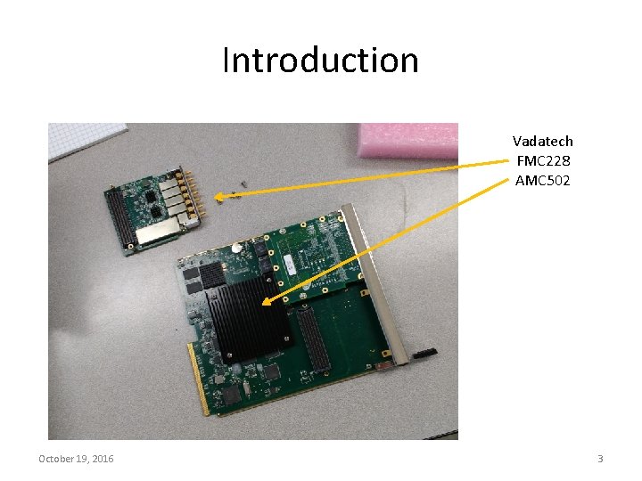
Introduction Vadatech FMC 228 AMC 502 October 19, 2016 3
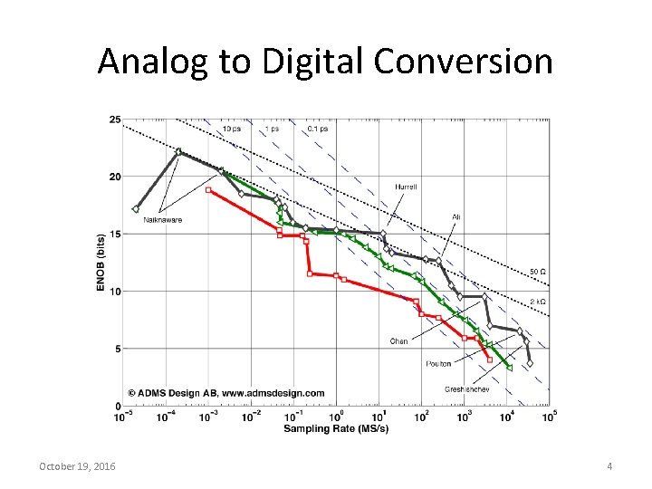
Analog to Digital Conversion October 19, 2016 4
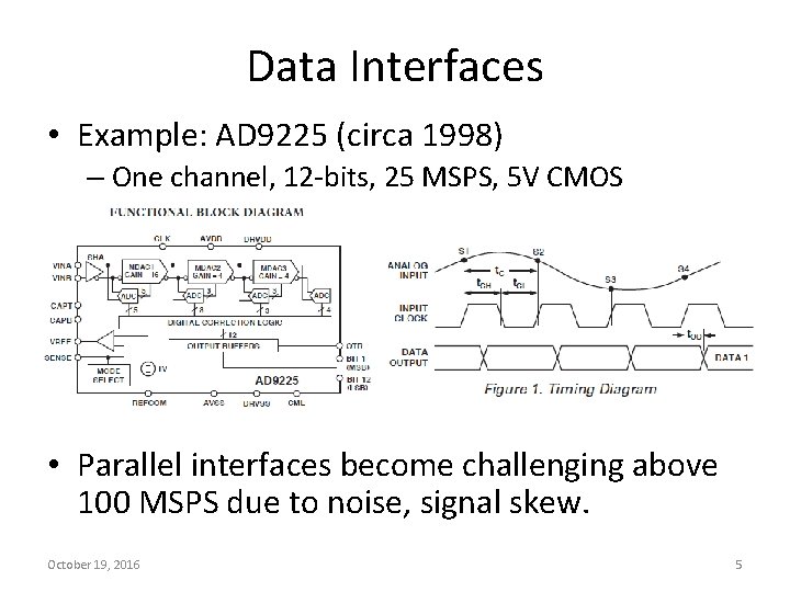
Data Interfaces • Example: AD 9225 (circa 1998) – One channel, 12 -bits, 25 MSPS, 5 V CMOS • Parallel interfaces become challenging above 100 MSPS due to noise, signal skew. October 19, 2016 5
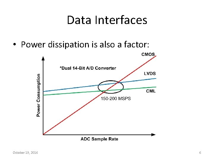
Data Interfaces • Power dissipation is also a factor: October 19, 2016 6
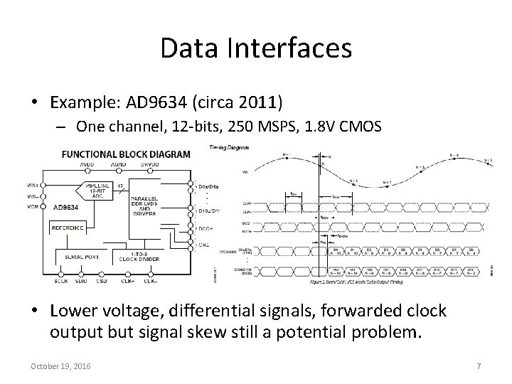
Data Interfaces • Example: AD 9634 (circa 2011) – One channel, 12 -bits, 250 MSPS, 1. 8 V CMOS • Lower voltage, differential signals, forwarded clock output but signal skew still a potential problem. October 19, 2016 7
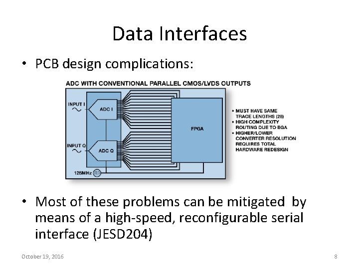
Data Interfaces • PCB design complications: • Most of these problems can be mitigated by means of a high-speed, reconfigurable serial interface (JESD 204) October 19, 2016 8
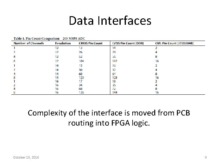
Data Interfaces Complexity of the interface is moved from PCB routing into FPGA logic. October 19, 2016 9
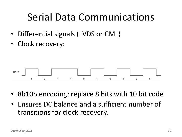
Serial Data Communications • Differential signals (LVDS or CML) • Clock recovery: • 8 b 10 b encoding: replace 8 bits with 10 bit code • Ensures DC balance and a sufficient number of transitions for clock recovery. October 19, 2016 10
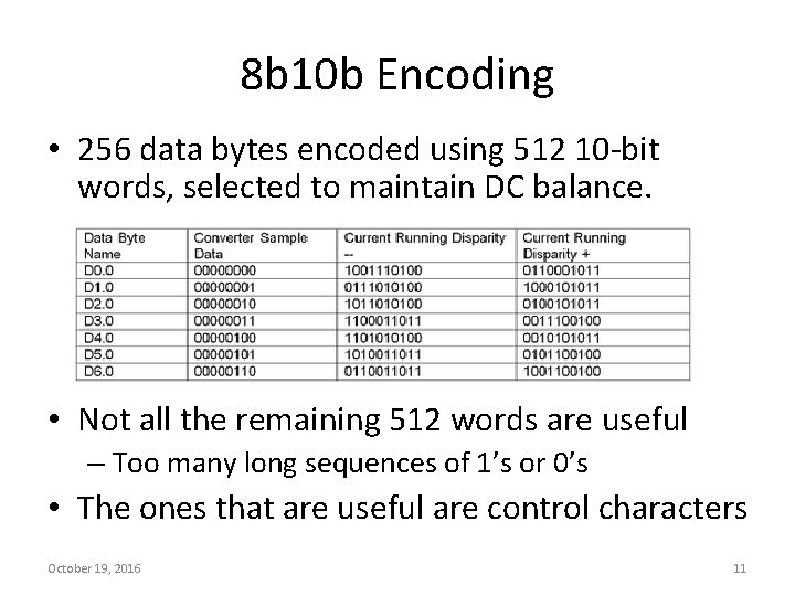
8 b 10 b Encoding • 256 data bytes encoded using 512 10 -bit words, selected to maintain DC balance. • Not all the remaining 512 words are useful – Too many long sequences of 1’s or 0’s • The ones that are useful are control characters October 19, 2016 11
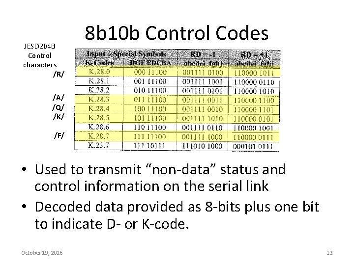
JESD 204 B Control characters /R/ 8 b 10 b Control Codes /A/ /Q/ /K/ /F/ • Used to transmit “non-data” status and control information on the serial link • Decoded data provided as 8 -bits plus one bit to indicate D- or K-code. October 19, 2016 12
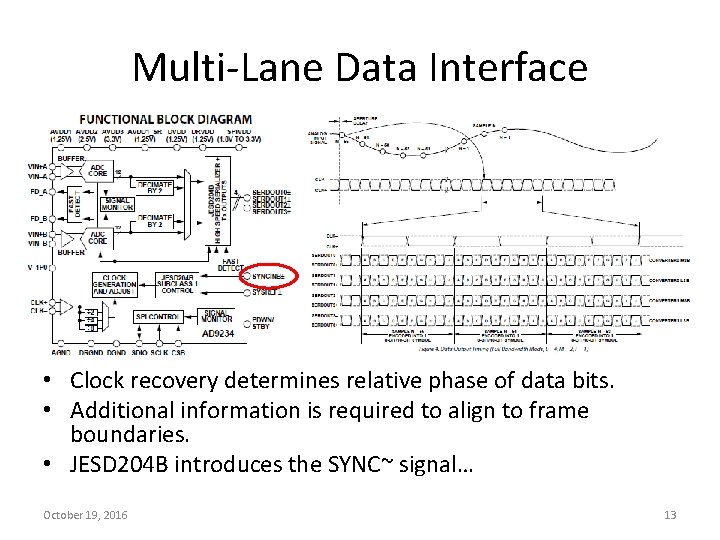
Multi-Lane Data Interface • Clock recovery determines relative phase of data bits. • Additional information is required to align to frame boundaries. • JESD 204 B introduces the SYNC~ signal… October 19, 2016 13
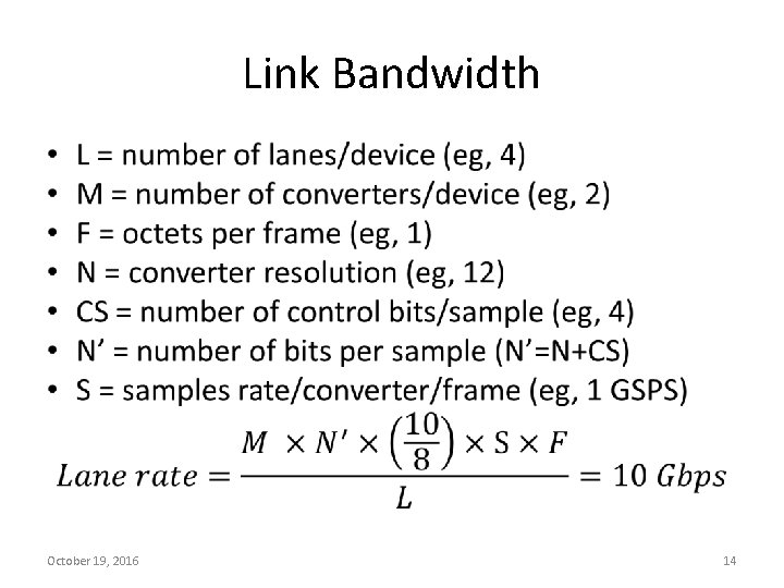
Link Bandwidth • October 19, 2016 14
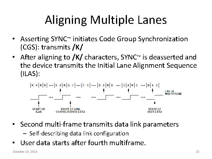
Aligning Multiple Lanes • Asserting SYNC~ initiates Code Group Synchronization (CGS): transmits /K/ • After aligning to /K/ characters, SYNC~ is deasserted and the device transmits the Initial Lane Alignment Sequence (ILAS): • Second multi-frame transmits data link parameters – Self-describing data link configuration • User data starts after fourth multiframe. October 19, 2016 15
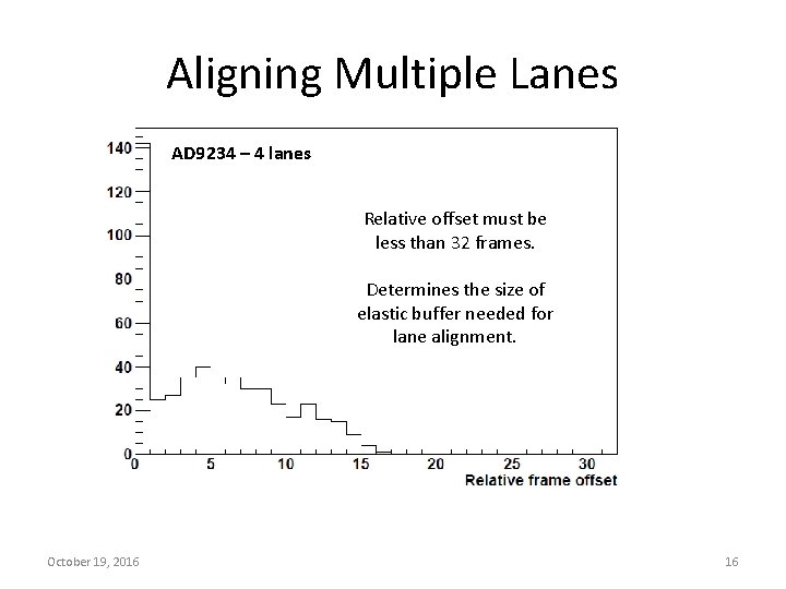
Aligning Multiple Lanes AD 9234 – 4 lanes Relative offset must be less than 32 frames. Determines the size of elastic buffer needed for lane alignment. October 19, 2016 16
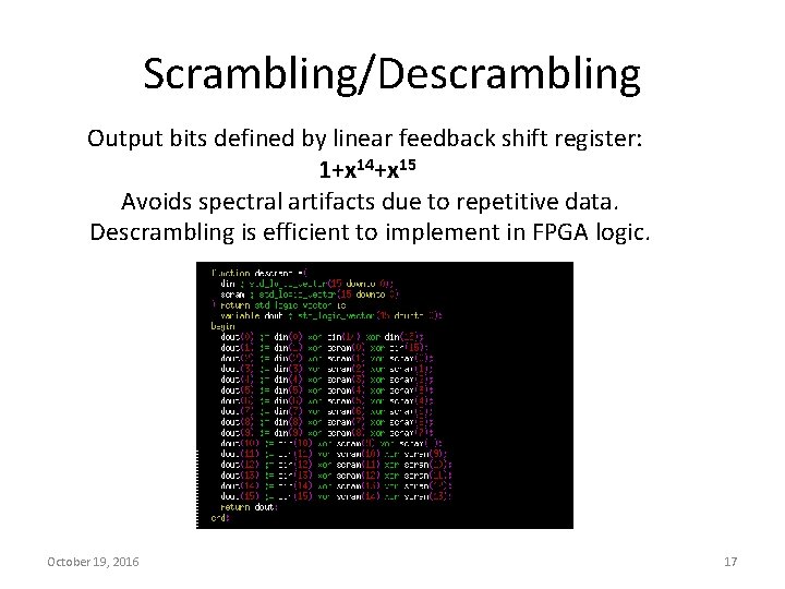
Scrambling/Descrambling Output bits defined by linear feedback shift register: 1+x 14+x 15 Avoids spectral artifacts due to repetitive data. Descrambling is efficient to implement in FPGA logic. October 19, 2016 17
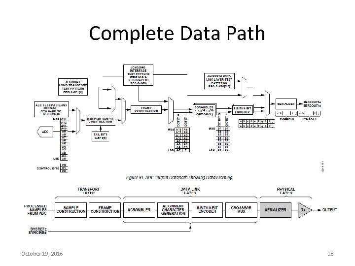
Complete Data Path October 19, 2016 18
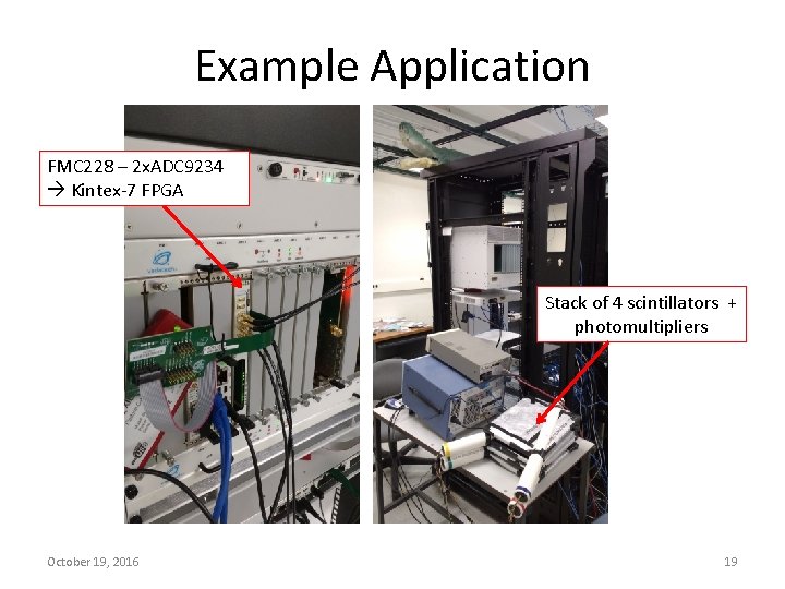
Example Application FMC 228 – 2 x. ADC 9234 Kintex-7 FPGA Stack of 4 scintillators + photomultipliers October 19, 2016 19
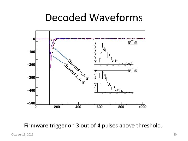
Decoded Waveforms Ch Ch an an ne ne l 0 l 1 : A , B Firmware trigger on 3 out of 4 pulses above threshold. October 19, 2016 20
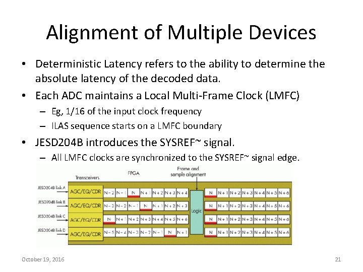
Alignment of Multiple Devices • Deterministic Latency refers to the ability to determine the absolute latency of the decoded data. • Each ADC maintains a Local Multi-Frame Clock (LMFC) – Eg, 1/16 of the input clock frequency – ILAS sequence starts on a LMFC boundary • JESD 204 B introduces the SYSREF~ signal. – All LMFC clocks are synchronized to the SYSREF~ signal edge. October 19, 2016 21
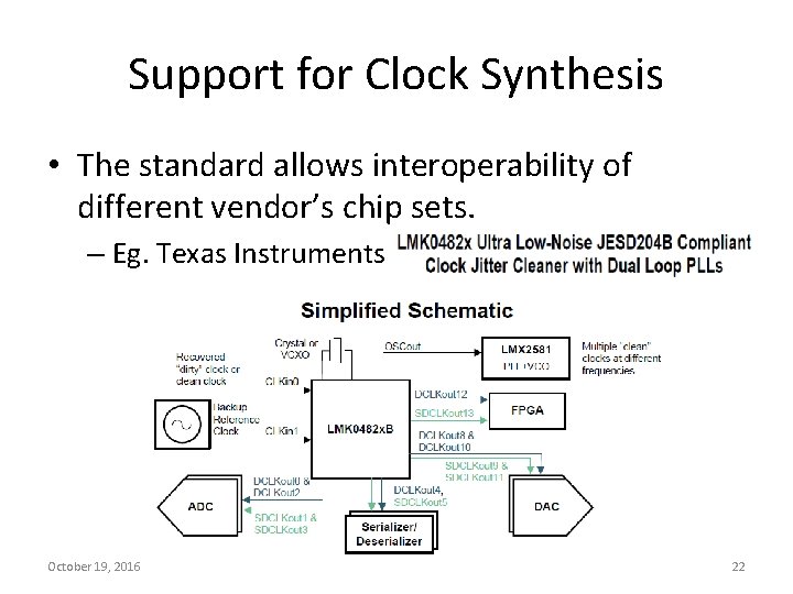
Support for Clock Synthesis • The standard allows interoperability of different vendor’s chip sets. – Eg. Texas Instruments October 19, 2016 22
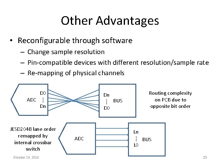
Other Advantages • Reconfigurable through software – Change sample resolution – Pin-compatible devices with different resolution/sample rate – Re-mapping of physical channels D 0 ADC ⁞ Dn JESD 204 B lane order remapped by internal crossbar switch October 19, 2016 Dn ⁞ BUS D 0 ADC Routing complexity on PCB due to opposite bit order Ln ⁞ BUS L 0 23
Comments • Deterministic latency is not the same as low latency – LVDS may still be more appropriate in cases where low latency is of primary concern • Same issues apply to high speed DAC’s driven by an FPGA • Potentially interesting for high-speed serial interfaces exchanging trigger data – No need to transmit bunch crossing counter with each data frame October 19, 2016 24
Hardware/Firmware Support • Hardware: – – – Analog Devices Texas Instruments Intersil Linear Technology Others… • Firmware vendors: – Xilinx: • JESD 204 PHY v 3. 2 (free): physical interface • JESD 204 core (licensed): bus interface – Altera: • JESD 204 B IP Core (licensed) October 19, 2016 25
Summary • The JESD 204 B standard is widely applicable to high-speed ADC and DAC applications • Widely accepted by industry • Solves several problems common to similar DAQ models – High speed, low noise, low power – Deterministic latency – Versatile, reconfigurable links • Applicable beyond ADC/DAC interfaces • Implementation is not all that difficult but working examples can be quite helpful October 19, 2016 26
- Slides: 26