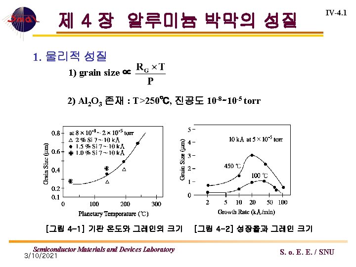
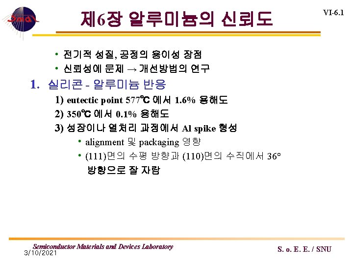
IV4 2 Grain Size 4 3 Semiconductor Materials
![IV-4. 2 Grain Size [그림 4 -3] 진공도와 기판온도가 그레인 크기에 미치는 영향 Semiconductor](https://slidetodoc.com/presentation_image_h/315580e56d18c68225fee41c82a525ba/image-2.jpg "IV-4. 2 Grain Size [그림 4 -3] 진공도와 기판온도가 그레인 크기에 미치는 영향 Semiconductor")
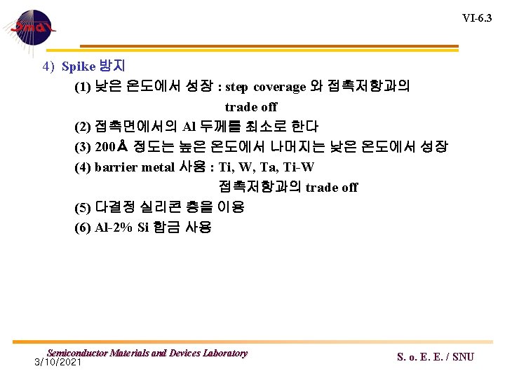
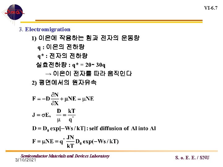
 Hillock 형성 (1) 형성 : 박막성장 및 아닐링 과정에서 생성 (2)")
![Hillock의 형태 IV-4. 4 [그림 4 -4] 세 가지 다른 그레인 형태의 hillock Semiconductor](https://slidetodoc.com/presentation_image_h/315580e56d18c68225fee41c82a525ba/image-4.jpg "Hillock의 형태 IV-4. 4 [그림 4 -4] 세 가지 다른 그레인 형태의 hillock Semiconductor")
 Hillock 의 방지 (1) self-diffusion rate 억제 : Sn, Cd, In")
![IV-4. 6 [표 4 -1] 어닐링 힐록의 밀도 Te(℃) Ta(℃) Dcycled( /㎠) Duncycled (](https://slidetodoc.com/presentation_image_h/315580e56d18c68225fee41c82a525ba/image-6.jpg "IV-4. 6 [표 4 -1] 어닐링 힐록의 밀도 Te(℃) Ta(℃) Dcycled( /㎠) Duncycled (")
 접촉저항 : 10 -5 ·cm 2/25× 25 m")
![IV-4. 8 [그림 4 -5] N형 실리콘에서 접촉저항 Semiconductor Materials and Devices Laboratory 3/10/2021](https://slidetodoc.com/presentation_image_h/315580e56d18c68225fee41c82a525ba/image-8.jpg "IV-4. 8 [그림 4 -5] N형 실리콘에서 접촉저항 Semiconductor Materials and Devices Laboratory 3/10/2021")
![IV-4. 9 [표 4 -2] 금속의 비저항 metal specific resistance(μΩ · cm) metal specific](https://slidetodoc.com/presentation_image_h/315580e56d18c68225fee41c82a525ba/image-9.jpg "IV-4. 9 [표 4 -2] 금속의 비저항 metal specific resistance(μΩ · cm) metal specific")
 챔버 내의 기체: O 2, H 2 O,")
![IV-4. 11 [표 4 -3] 금속의 산화에 필요한 생성 에너지 oxide heat of formation(kcal/mole)](https://slidetodoc.com/presentation_image_h/315580e56d18c68225fee41c82a525ba/image-11.jpg "IV-4. 11 [표 4 -3] 금속의 산화에 필요한 생성 에너지 oxide heat of formation(kcal/mole)")
 Shadowing : slope, geometric, self shadowing Shadow 형성:")
 Shadowing 의 최소화 방법 • deposition system의 설계 최적화 • biaxial")
![Biaxial plenatary IV-4. 14 [그림 4 -8] 소스와 기판 사이의 기하학적 관계 Semiconductor Materials](https://slidetodoc.com/presentation_image_h/315580e56d18c68225fee41c82a525ba/image-14.jpg "Biaxial plenatary IV-4. 14 [그림 4 -8] 소스와 기판 사이의 기하학적 관계 Semiconductor Materials")
 Si. O 2 와의 접착 2) 간단한 접착 시험")
 장점 : 단일층 박막, low cost, high")
![제 5장 알루미늄의 공정 V-5. 1 1. double metal 공정 [그림 5 -1] 이층](https://slidetodoc.com/presentation_image_h/315580e56d18c68225fee41c82a525ba/image-17.jpg "제 5장 알루미늄의 공정 V-5. 1 1. double metal 공정 [그림 5 -1] 이층")
 1 st metal 공정 • Al, Al-Si, Al-Cu, Al-Si-Cu • 막형성")
 Sharp edge : 성장핵의 형성으로 막성장이")
![V-5. 4 [그림 5 -2] 힐록에 의한 금속의 합선 Semiconductor Materials and Devices Laboratory](https://slidetodoc.com/presentation_image_h/315580e56d18c68225fee41c82a525ba/image-20.jpg "V-5. 4 [그림 5 -2] 힐록에 의한 금속의 합선 Semiconductor Materials and Devices Laboratory")
 경사 식각 : hard baking 조절로")
![V-5. 6 6. 양극 산화 1) 양극 산화공정 [그림 5 -3] 양극 산화의 장치](https://slidetodoc.com/presentation_image_h/315580e56d18c68225fee41c82a525ba/image-22.jpg "V-5. 6 6. 양극 산화 1) 양극 산화공정 [그림 5 -3] 양극 산화의 장치")
![V-5. 7 [그림 5 -4] H 3 PO 4 전해액에서의 Al의 양극 산화 특성](https://slidetodoc.com/presentation_image_h/315580e56d18c68225fee41c82a525ba/image-23.jpg "V-5. 7 [그림 5 -4] H 3 PO 4 전해액에서의 Al의 양극 산화 특성")
![V-5. 9 4) 다공질 양극산화 [그림 5 -5] 전압이 다공질 Al 2 O 3에](https://slidetodoc.com/presentation_image_h/315580e56d18c68225fee41c82a525ba/image-25.jpg "V-5. 9 4) 다공질 양극산화 [그림 5 -5] 전압이 다공질 Al 2 O 3에")
 낮은 전압 : 기공의 밀도가 커지며 강도는 낮아진다 (2) 전압은 전해액에")
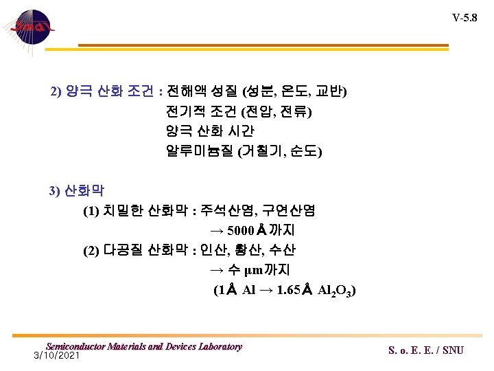
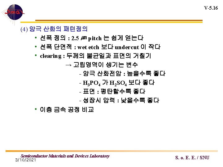
 양극 산화 마스크 • 마스킹 재료 : PR(저압<160 V) 저온 CVD")
![V-5. 13 [그림 5 -7] 25℃, 4 % H 2 SO 4에서의 Al의 양극](https://slidetodoc.com/presentation_image_h/315580e56d18c68225fee41c82a525ba/image-29.jpg "V-5. 13 [그림 5 -7] 25℃, 4 % H 2 SO 4에서의 Al의 양극")
![V-5. 14 [그림 5 -8] 25℃, 4 % H 3 PO 4에서의 Al의 양극](https://slidetodoc.com/presentation_image_h/315580e56d18c68225fee41c82a525ba/image-30.jpg "V-5. 14 [그림 5 -8] 25℃, 4 % H 3 PO 4에서의 Al의 양극")
![V-5. 15 [그림 5 -9] 전압을 제한시킨 4 % H 3 PO 4에서의 Al의](https://slidetodoc.com/presentation_image_h/315580e56d18c68225fee41c82a525ba/image-31.jpg "V-5. 15 [그림 5 -9] 전압을 제한시킨 4 % H 3 PO 4에서의 Al의")
![V-5. 17 [표 5 -2] 양극 산화와 습식 에치를 이용한 이층 금속 공정의 비교](https://slidetodoc.com/presentation_image_h/315580e56d18c68225fee41c82a525ba/image-33.jpg "V-5. 17 [표 5 -2] 양극 산화와 습식 에치를 이용한 이층 금속 공정의 비교")
![VI-6. 2 [그림 6 -1] Si의 Al에서의 용해도 Semiconductor Materials and Devices Laboratory 3/10/2021](https://slidetodoc.com/presentation_image_h/315580e56d18c68225fee41c82a525ba/image-35.jpg "VI-6. 2 [그림 6 -1] Si의 Al에서의 용해도 Semiconductor Materials and Devices Laboratory 3/10/2021")
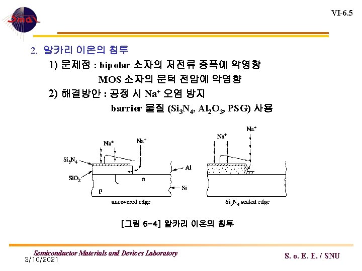
![VI-6. 6 [그림 6 -5] 알카리 이온을 막기 위한 Al 2 O 3 박막](https://slidetodoc.com/presentation_image_h/315580e56d18c68225fee41c82a525ba/image-39.jpg "VI-6. 6 [그림 6 -5] 알카리 이온을 막기 위한 Al 2 O 3 박막")
 원자가 쌓이거나 공핍되는 원인 (1) 온도 : temperature gradient (2) diffusion")
 Electromigration 에 의한 MTF (1) MTF 변화요인 • 선폭 단면적에 따라")
![VI-6. 10 [표 6 -1] MTF의 향상 grain size: large(>3μm) small(<1μm) surface coating: Al](https://slidetodoc.com/presentation_image_h/315580e56d18c68225fee41c82a525ba/image-43.jpg "VI-6. 10 [표 6 -1] MTF의 향상 grain size: large(>3μm) small(<1μm) surface coating: Al")
 plastic package 에서 발생 (2) 전기화학적 부식 : H")
![부식 시험 VI-6. 12 [그림 6 -6] 부식 시험 계략도 Semiconductor Materials and Devices](https://slidetodoc.com/presentation_image_h/315580e56d18c68225fee41c82a525ba/image-45.jpg "부식 시험 VI-6. 12 [그림 6 -6] 부식 시험 계략도 Semiconductor Materials and Devices")
![VI-6. 13 corrosion rates [그림 6 -7] 인의 양과 부식 Semiconductor Materials and Devices](https://slidetodoc.com/presentation_image_h/315580e56d18c68225fee41c82a525ba/image-46.jpg "VI-6. 13 corrosion rates [그림 6 -7] 인의 양과 부식 Semiconductor Materials and Devices")
- Slides: 46
IV-4. 2 Grain Size [그림 4 -3] 진공도와 기판온도가 그레인 크기에 미치는 영향 Semiconductor Materials and Devices Laboratory 3/10/2021 S. o. E. E. / SNU
IV-4. 3 2) Hillock 형성 (1) 형성 : 박막성장 및 아닐링 과정에서 생성 (2) Hillock 의 형태 : edge, flat-topped, spike hillock (3) 원인 : 실리콘과 Al의 stress 와 strain • 온도상승하면 질량이동하여 stress 감소 선팽창계수 : Si (3. 3 ppm/℃), Al (23. 6 ppm/℃) • 막형성 온도 (Te)와 아닐링 온도(Ta) 차이 → strain Semiconductor Materials and Devices Laboratory 3/10/2021 S. o. E. E. / SNU
Hillock의 형태 IV-4. 4 [그림 4 -4] 세 가지 다른 그레인 형태의 hillock Semiconductor Materials and Devices Laboratory 3/10/2021 S. o. E. E. / SNU
IV-4. 5 3) Hillock 의 방지 (1) self-diffusion rate 억제 : Sn, Cd, In (2) 핵형성 site 제공 : Si (3) hillock 의 영향 : 신뢰도를 떨어뜨린다 • 얇아진 부분에서 열이 발생하고 더욱 얇아져 끊어짐 Semiconductor Materials and Devices Laboratory 3/10/2021 S. o. E. E. / SNU
IV-4. 6 [표 4 -1] 어닐링 힐록의 밀도 Te(℃) Ta(℃) Dcycled( /㎠) Duncycled ( /㎠) 23 430 8. 7× 10⁷ 4. 0 × 107 200 430 1. 5 × 10⁶ 5. 0 × 105 400 430 3. 4 × 10⁴ 6. 0 × 103 27 223 6. 0 × 106 3. 2 × 10⁶ 200 179 5. 2 × 10⁵ 2. 8 × 10⁵ 400 237 0 0 Note : 1) uncycled : RT → Ta 일회 2) cycled : RT → Ta 반복 Semiconductor Materials and Devices Laboratory 3/10/2021 S. o. E. E. / SNU
IV-4. 7 2. 전기적 성질 1) 접촉저항 : 10 -5 ·cm 2/25× 25 m 2 2) 열처리 : 500℃, 10 min. 450℃, 30 min. 3) 비저항 : Al (2. 65 ·cm), Al-Si (1%)(3. 0 ·cm) 4) ρ> 0. 002 Ω·㎝ ( 5× 10¹⁹ dopants/cm 3 ) → rectifying contact (확산 그림 1– 7 및 금속 그림 2 -10 참조) Semiconductor Materials and Devices Laboratory 3/10/2021 S. o. E. E. / SNU
IV-4. 8 [그림 4 -5] N형 실리콘에서 접촉저항 Semiconductor Materials and Devices Laboratory 3/10/2021 [그림 4 -6] P형 실리콘에서의 접촉 저항 S. o. E. E. / SNU
IV-4. 9 [표 4 -2] 금속의 비저항 metal specific resistance(μΩ · cm) metal specific resistance (μΩ · cm) Au 2. 35 Al-Ni(1%) 2. 75 Al 2. 65 Al-Si(1%) 3. 0 Mo 5. 7 Al-Ti(1%) 5. 53 Pt 10. 6 Al-Cr(1%) 5. 78 Ti 55. 0 Al-Pt(1%) 2. 9 Au. Ni(10%) 10. 2 Semiconductor Materials and Devices Laboratory 3/10/2021 S. o. E. E. / SNU
IV-4. 10 3. 화학적 성질 1) 챔버 내의 기체: O 2, H 2 O, H 2, N 2, CH 4 2) 주요 기체 : H 2 O, O 2 2 Al + 3 O 2 = 2 Al 2 O 3 3) 열처리 : 낮은 저항의 접촉면 형성 3 Si. O 2 + 2 Al → 2 Al 2 O 3 + 3 Si (실리콘이 Al으로 확산 → alloy 형성) Semiconductor Materials and Devices Laboratory 3/10/2021 S. o. E. E. / SNU
IV-4. 11 [표 4 -3] 금속의 산화에 필요한 생성 에너지 oxide heat of formation(kcal/mole) oxide heat of formation(kcal/mole ) Ta 2 O 5 -500 WO 3 -200 Al 2 O 3 -399 Mo. O 3 -180 V 2 O 3 -290 Cu 2 O -40 Cr 2 O 3 -270 Ag 2 O -7 Ti. O 2 -218 Au 2 O 3 +19 Si. O 2 -205 Semiconductor Materials and Devices Laboratory 3/10/2021 S. o. E. E. / SNU
IV-4. 12 4. 표면 Coverage 1) Shadowing : slope, geometric, self shadowing Shadow 형성: [그림 4 -7] 소스와 기판의 기하학적인 관계 Semiconductor Materials and Devices Laboratory 3/10/2021 S. o. E. E. / SNU
IV-4. 13 2) Shadowing 의 최소화 방법 • deposition system의 설계 최적화 • biaxial plenatary 사용 • source 의 면적을 크게 • source - substrate 간격 크게 • 기판 온도 높이고 • 기판 패턴의 경사각을 작게 Semiconductor Materials and Devices Laboratory 3/10/2021 S. o. E. E. / SNU
Biaxial plenatary IV-4. 14 [그림 4 -8] 소스와 기판 사이의 기하학적 관계 Semiconductor Materials and Devices Laboratory 3/10/2021 S. o. E. E. / SNU
IV-4. 15 5. Adhesion 1) Si. O 2 와의 접착 2) 간단한 접착 시험 : tape(3 M) 시험 [표 4 -4] 금속 및 실리사이드의 실리콘 산화막과의 접착성 materials shearing force(108 dynes/cm 2) adherence to Si. O 2 Fe. Si 37 weak Co. Si 120 strong Co. Si 2 70 intermediate Pt. Si 2 170 very strong Al 170 very strong Ti 170 very strong Au - very weak Co 54 intermediate Mo 113 strong Semiconductor Materials and Devices Laboratory 3/10/2021 S. o. E. E. / SNU
IV-4. 16 6. 알루미늄 시스템의 장단점 1) 장점 : 단일층 박막, low cost, high conductivity 간단한 박막형성, good adhesion, easy patterning, low contact resistance, Al-Si alloy 이용, good bondability, 대기중의 산화가 어렵다. 유연성이 좋다 2) 단점: difficult CVD deposition, 전기도금이 어렵다 electromigration, corrosion, hillock formation, Al-Au 접합부분에서의 반응 → 전기 전도도가 낮아진다, Si into Al grain boundary → reliability, silicon 보다 높은 열팽창계수 → stress , 쉽게 긁힘 Semiconductor Materials and Devices Laboratory 3/10/2021 S. o. E. E. / SNU
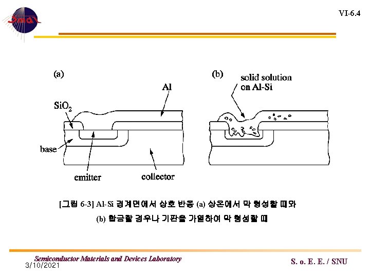
제 5장 알루미늄의 공정 V-5. 1 1. double metal 공정 [그림 5 -1] 이층 금속 공정의 예 Semiconductor Materials and Devices Laboratory 3/10/2021 S. o. E. E. / SNU
V-5. 2 1) 1 st metal 공정 • Al, Al-Si, Al-Cu, Al-Si-Cu • 막형성 Al : E-beam, sputtering Al-Si : double gun E-beam, sputtering Al-Si-Cu : flash, sputtering 2) 1 st insulator • Si. O 2, Si 3 N 4, Al 2 O 3, Ta 2 O 5, WO 2, PSG • 막형성 : CVD, sputtering 3) 2 nd metal • Al 또는 1 st metal과 동일 4) passivation • PSG : 3% 인도핑 , 0. 8~1μm 두께, 85 Å/sec : 35 Å/sec for PSG : CVD 산화막(식각률) Semiconductor Materials and Devices Laboratory 3/10/2021 S. o. E. E. / SNU
V-5. 3 3. 이층 금속 공정 문제점 1) Sharp edge : 성장핵의 형성으로 막성장이 빨라짐 • 1 st & 2 nd metal 의 short • 2 nd metal crack → reliability 2) Hillock 형성 • Al deposition 할 때 (380℃) • PSG deposition (200℃) in alloy (450℃) 3) Si. O 2 미립자 : chamber 내에서 핵 형성, Al film 에 들어감. 4) 재작업 불가 Semiconductor Materials and Devices Laboratory 3/10/2021 S. o. E. E. / SNU
V-5. 4 [그림 5 -2] 힐록에 의한 금속의 합선 Semiconductor Materials and Devices Laboratory 3/10/2021 S. o. E. E. / SNU
V-5. 5 4. Sharp edge 문제 해결 1) 경사 식각 : hard baking 조절로 감광막이 etch 동안 일어나게 함 2) 녹는 마스크물질의 코팅 3) hillock 문제 : 저온 성장, Al-Si 사용 4) PECVD Si. O 2 deposition : 열 CVD system 보다 Si. O 2 핵형성에 의한 입자의 contamination 적음. 5. 기타 알루미늄 공정 • 양극 산화 • 유기물 절연체 : polymide → 산소 plasma etching Semiconductor Materials and Devices Laboratory 3/10/2021 S. o. E. E. / SNU
V-5. 6 6. 양극 산화 1) 양극 산화공정 [그림 5 -3] 양극 산화의 장치 Semiconductor Materials and Devices Laboratory 3/10/2021 S. o. E. E. / SNU
V-5. 7 [그림 5 -4] H 3 PO 4 전해액에서의 Al의 양극 산화 특성 Semiconductor Materials and Devices Laboratory 3/10/2021 S. o. E. E. / SNU
V-5. 9 4) 다공질 양극산화 [그림 5 -5] 전압이 다공질 Al 2 O 3에 미치는 영향 Semiconductor Materials and Devices Laboratory 3/10/2021 S. o. E. E. / SNU
V-5. 10 (1) 낮은 전압 : 기공의 밀도가 커지며 강도는 낮아진다 (2) 전압은 전해액에 따라 조절 된다 (3) 산화막 성장은 Faraday 법칙에 따른다 V: 부피, ρ: 밀도, F : 96500 C/mole, m=6, S: 면적, H: 높이 M : mole 단위 질량, Q : 전체 전하, η : 효율, J : 전류밀도 [표 5 -1] 25℃, 10 m. A/cm 2에서의 다공질 양극 산화 high voltage low voltage Electrolyte 4 % H 3 PO 4 4 % H 2 SO 4 operating voltage 133 20 Barrier layer thickness(Å) 1, 500 250 Semiconductor Materials and Devices Laboratory 3/10/2021 S. o. E. E. / SNU
V-5. 12 (2) 양극 산화 마스크 • 마스킹 재료 : PR(저압<160 V) 저온 CVD 산화막, PSG 양극 산화막 Al 2 O 3 (3) 양극 산화의 특성 • current density : 10 m. A/cm 2 로 유지시킨다 • voltage : variable • time : 6 minutes for 1 μm Al Semiconductor Materials and Devices Laboratory 3/10/2021 S. o. E. E. / SNU
V-5. 13 [그림 5 -7] 25℃, 4 % H 2 SO 4에서의 Al의 양극 산화 특성 Semiconductor Materials and Devices Laboratory 3/10/2021 S. o. E. E. / SNU
V-5. 14 [그림 5 -8] 25℃, 4 % H 3 PO 4에서의 Al의 양극 산화 특성 Semiconductor Materials and Devices Laboratory 3/10/2021 S. o. E. E. / SNU
V-5. 15 [그림 5 -9] 전압을 제한시킨 4 % H 3 PO 4에서의 Al의 양극 산화 특성 Semiconductor Materials and Devices Laboratory 3/10/2021 S. o. E. E. / SNU
V-5. 17 [표 5 -2] 양극 산화와 습식 에치를 이용한 이층 금속 공정의 비교 anodization wet etch Al deposition PSG deposition masking exposure and bake PSG etch Al etch anodization PSG deposition masking via etch double metal process Semiconductor Materials and Devices Laboratory 3/10/2021 S. o. E. E. / SNU
VI-6. 2 [그림 6 -1] Si의 Al에서의 용해도 Semiconductor Materials and Devices Laboratory 3/10/2021 S. o. E. E. / SNU
VI-6. 6 [그림 6 -5] 알카리 이온을 막기 위한 Al 2 O 3 박막 Semiconductor Materials and Devices Laboratory 3/10/2021 S. o. E. E. / SNU
VI-6. 8 3) 원자가 쌓이거나 공핍되는 원인 (1) 온도 : temperature gradient (2) diffusion : surface diffusion grain boundary diffusion bulk diffusion (3) 활성화 에너지 변화 : grain 크기 변화 접촉근처의 성분 변화 : Do, Ws, J 변화 step 에서의 current crowding Semiconductor Materials and Devices Laboratory 3/10/2021 S. o. E. E. / SNU
VI-6. 9 4) Electromigration 에 의한 MTF (1) MTF 변화요인 • 선폭 단면적에 따라 증가 • 선의 길이에 따라 감소 • 원자 유속에 반비례 MTF ∝ W : Al 선폭 , n : 1 T : Al 두께 (contact), 2∼ 3 (선) (2) MTF 향상 Semiconductor Materials and Devices Laboratory 3/10/2021 S. o. E. E. / SNU
VI-6. 10 [표 6 -1] MTF의 향상 grain size: large(>3μm) small(<1μm) surface coating: Al 2 O 3(anodized) Si. O 2(CVD) additives to Al : (1~2)% Si (4~6)% Cu, Mg, Cr Semiconductor Materials and Devices Laboratory 3/10/2021 MTF Ws(e. V) 2~3 0. 5 ~ 0. 6 1 0. 3 ~ 0. 4 10 ~ 14 0. 6 ~ 0. 65 1~2 1 10 ~ 100 0. 7 ~ 0. 8 S. o. E. E. / SNU
VI-6. 11 4. Corrosion (1) plastic package 에서 발생 (2) 전기화학적 부식 : H 2 O, P, 전장 (3) corrosion test : 1000시간, 1 V/㎛ Al/Si. O 2, Al/Si 3 N 4/Si. O 2 : No Al/PSG/Si. O 2, PSG/Al/Si. O 2 : Yes H 2 O + PSG → H 3 PO 4 (4) 방지책 : LTO/PSG/LTO layer 사용 (crack 이 생기는 것에 주의) Semiconductor Materials and Devices Laboratory 3/10/2021 S. o. E. E. / SNU
부식 시험 VI-6. 12 [그림 6 -6] 부식 시험 계략도 Semiconductor Materials and Devices Laboratory 3/10/2021 S. o. E. E. / SNU
VI-6. 13 corrosion rates [그림 6 -7] 인의 양과 부식 Semiconductor Materials and Devices Laboratory 3/10/2021 [그림 6 -8] 전장의 세기와 부식 S. o. E. E. / SNU