Isp LEVER 6 1 Schematic Table of Contents
")
Isp. LEVER 6. 1 을 이용한 회로 설계(Schematic)

Table of Contents 1. isp. LEVER 6. 1 tool의 시작프로그램 2. Lattice Device의 Design 1) 프로그램시작 2) 새로운 Project 만들기 3) isp. LEVER 6. 1 의 Main Window 4) Device 선정하기 Design Source 만들기 1) Schematic Design Example * Drawing Toolbar icons기능 1 -1 Schematic Design (4 Bit Up Counter) 1 -2 Pin Locking (Constraint Manager 이용) 1 -3 Pin Locking (Schematic Design Source) 1 -4 Compile 1 -5 Simulation isp. LEVER 6. 1

1. isp. LEVER 6. 1의 시작프로그램 지금의 isp. LEVER tool은 Lattice License Adapter라는 가상의 네트워크 Adapter를 설치하여 사용하고 있습니다 * Isp. LEVER Project Navigator -> Lattice의 모든 Device지원 -> Schematic, ABEL, VHDL, Verilog HDL, EDIF -> Timing, Function Simulation -> Compile -> isp. Download * isp. LEVER Registration and License Request -> License Request Form의 작성 * isp. UPDATE -> Web과 연결되어 Tool Update * sp. VM System -> isp. Download Program ABEL/Schematic VHDL/Schematic Verilog/Schematic의 혼용Design 지원 ABEL(Used with CPLDs only. ) GDF (Used with isp. GDX device only. )
 or")
1. isp. LEVER 6. 1의 시작프로그램 ->Runs the Design Planner (for FPGA designs) or Floorplanner (for isp. XPGA designs), ->EPIC Device Editor ->Module/IP Manager ->Runs the Power Calculator, which allows you to calculate power consumption for some Lattice devices Legacy Constraints Translator -> isp. LEVER Program이전에 존재했었던 구 버전의 (isp. EXPERT ) 프로그램과 일부 File체계가 달라서 다른 파일들을 isp. LEVER에 맞게 Conversion해주는 메뉴 Model. Sim -> HDL Simulation ->Runs the Precision synthesis tool for VHDL/Verilog synthesis ->Runs the Synplify synthesis tool for VHDL/Verilog synthesis
 프로그램시작 Window시작->프로그램(P) -> Lattice Semiconductor에서 isp. LEVER Project Navigator를실행 ->Close")
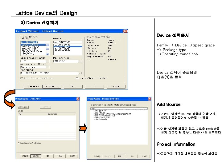
Lattice Device의 Design 1) 프로그램시작 Window시작->프로그램(P) -> Lattice Semiconductor에서 isp. LEVER Project Navigator를실행 ->Close 된Project ->보통 이전에 작업한Project가 있으면 그 Project가 올라옴. -> New Project -> Open Project
 새로운 Project 만들기 File->New Project를 선택 Project는~. syn으로 저장되며 project")
Lattice Device의 Design 2) 새로운 Project 만들기 File->New Project를 선택 Project는~. syn으로 저장되며 project name과 Design Entry Type과 Synthesis Tools을 선택하고 다음(N) 버튼을 누른다 ABEL/Schematic VHDL/Schematic Verilog/Schematic의 혼용Design 지원
 Schematic Design Example 1)Source ->New 선택 NEW ->새로운")
Lattice Device의 Design Source 만들기 1) Schematic Design Example 1)Source ->New 선택 NEW ->새로운 source만들기 Import ->기존에 설계된 source를 불러오기 2) Design 형태를 선택 ABEL Test Vectors ->ABEL로 Design한 경우 Simulation 하기 위한 Text Editor Schematic ->Schematic을 이용한 Design VHDL Module ->VHDL Editor Waveform Stimulus ->Simulation용 Waveform Editor
 Schematic Editor의 Main Window Drawing Toolbar ->만약Drawing Toolbar가 나타나지 않으며,")
Lattice Device의 Design 3) Schematic Editor의 Main Window Drawing Toolbar ->만약Drawing Toolbar가 나타나지 않으며, View ->Draw Toolbar를 선택하십시오 Schematic File Name ->file name 입력

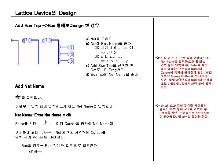
Lattice Device의 Design Drawing Toolbar Icon 기능 Add Symbol -> Basic Library , User Library를 불러옴 이때User에 의해 생성된 Symbol은 Local에 위치함 Add Wire Add Bus Tap Add Instance Name Add Net Name Add I/O Marker Edit Pin Attribute Edit Symbol Attribute Edit Net Attribute Duplicate Move Add Wire -> Symbol Net간 의결선 Drag Rotate Mirror Delete Draw Text Wire 결선 시 항상 사각형의 상자와 일치 시켜서 사각형의 상자가 사라져야 한다. Draw Line Draw Rectangle Draw Arc Draw Circle Highlight

Lattice Device의 Design ⑧ Add Block Symbol Use Data From This Block ->현재의Design을Symbol화함 Use Data From NAF File ->Design를 Save하면 확장자가 NAF인 파일이 생성되며, 이 파일을 읽어 들여 Symbol로 만든다 ⑨ VCC / GND ->VCC, GND는Symbol로 존재하는 것이 아니라, Net Name에 VCC또는 GND로 입력하면 된다. 이때 모양이 변화된다. ⑩ Design Title ->Add Symbol를 선택한 후C: ₩…₩GENERIC₩MISC를 선택, Title를 선택한 후 Mouse Click을 하면, 자동으로 하단우측에 정렬된다 File->Matching Symbol을 선택하면 현재의Design이 Symbol화 된다
 Pin Locking (Constraint Editor를 이용) ***입출력 핀 할당*** CPLD")
Lattice Device의 Design 1 -2) Pin Locking (Constraint Editor를 이용) ***입출력 핀 할당*** CPLD device Constraint Editor를 이용 FPGA device Design Planner (post-Map)를 이용 ->오른쪽 창에서 Input pins 또는 Output pins에서 pin을 선택한 후 드래그하여 왼쪽의 Top View의 빈자리에 넣어주면 Signal이 할당됨 오른쪽 pin Attributes창의 pin block을 Double click한 후 직접 입력하여도 Signal이 할당됨 (*signal을 할당할 때 device datasheet의 Pinout Information의 내용을 참조) ->할당된 pin을 해제하고자 할 때에는 Top View의 pin에서 마우스 오른쪽 버튼을 눌러 Unlock를 click하면 된다
 Pin Locking (Schematic Design Source 내에 직접입력) 1)Add Symbol을")
Lattice Device의 Design 1 -3) Pin Locking (Schematic Design Source 내에 직접입력) 1)Add Symbol을 실행한다 2)IOPADS. LIB를 선택한 후 원하는 해당I/O Pad를 선택하여 연결한다 3)Drawing tool bar에서 Symbol Attribute Editor을 선택한다 4)I/O Pad를 선택하면, 빗금으로 선택된다 5)Symbol Attribute Editor에서 Pin Number를 선택한 후, 원하는 Pin Number를 입력한다 *FPGA device같은 경우에 IOPADS. LIB를 제공하지 않기 때문에 1 -2에서처럼 Constraint Editor를 이용하여 Signal을 할당해야 함
 Compile (Fit Design) Process state Icon Initial No icon")
Lattice Device의 Design 1 -4) Compile (Fit Design) Process state Icon Initial No icon Warnings completed Errors Sources windows창에서 device를 선택하고 Fit Design을 Mouse Double-Click하여 compile을 실행하면 Output Panel에 Completed successfully. 과 함께 Processes Window에 표시되면 성공적으로 Compile된 것임. Fitter Report (text) 와 Fitter Report (html) 두 가지 메뉴를 통해서 compile결과를 확인할 수 있다.
 Simulation -> Source/New…/ Waveform Stimulus 를 선택 ->Top Design에")
Lattice Device의 Design 1 -5) Simulation -> Source/New…/ Waveform Stimulus 를 선택 ->Top Design에 대한 Timing Function Simulation을 원하는 경우는 Device 로 선택하며, 해당 Design에 대해서 Function Simulation을 원하는 경우 는 해당 Design Name을 선택한다.

Lattice Device의 Design -> Waveform Editor ->New Waveform Stimulus의 WDL File Name을 입력한다. 이때 File 확장자는 *. wdl임

Lattice Device의 Design -> Import Wave ->Waveform Editing을 하기 위한 Signal들을 불러드리기 위해서 Edit/Import Wave…를 선택한다 ->Simulation에 필요한 Signal들을 선택 Add 한 후, Show를 실행한 후 창을 닫는다. (Cancel)
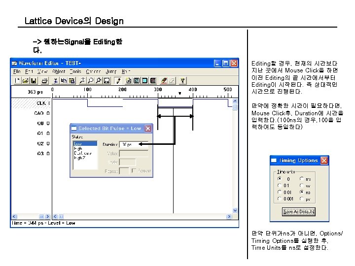
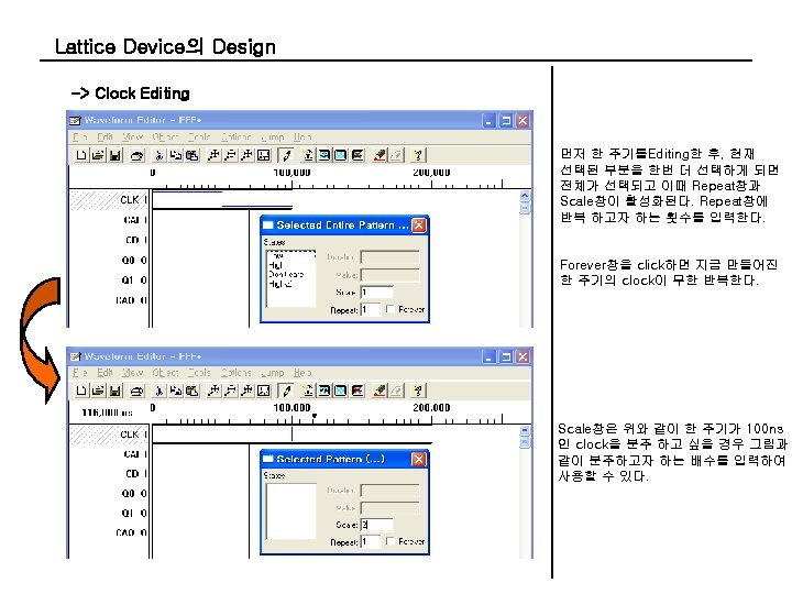

Lattice Device의 Design -> Simulation Waveform Editing이 완료되면 종료한 후 tool에 Editing된 WDL File이 등록되며, 원하는 Simulation을 Double-Click한다 Functional Simulation -> 단순히 Function만을 체크 Timing Simulation -> 칩의 타이밍정보를 고려해 Delay등을 체크

Lattice Device의 Design -> Simulator Control Panel에서 RUN을 클릭한다. -> Simulation 결과를 확인한다 Timing Simulation -> Delay된 값을 확인할 수 있다
- Slides: 24