ISA Design for the Project CS 3220 Fall

![Instruction Format Thus Far wire [3: 0] op 1; // Primary opcode wire [3: Instruction Format Thus Far wire [3: 0] op 1; // Primary opcode wire [3:](https://slidetodoc.com/presentation_image_h/8d90efa991e16576ddd298649b209a70/image-13.jpg)


- Slides: 33

ISA Design for the Project CS 3220 Fall 2014 Hadi Esmaeilzadeh hadi@cc. gatech. edu Georgia Institute of Technology Some slides adopted from Prof. Milos Prvulovic

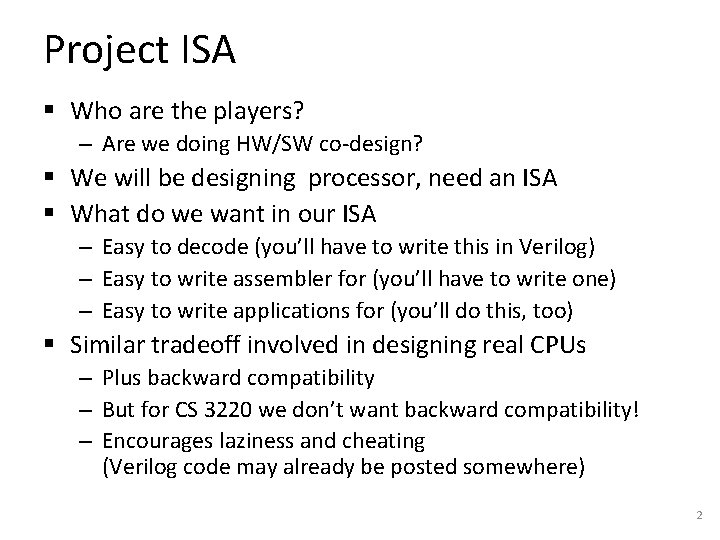
Project ISA § Who are the players? – Are we doing HW/SW co-design? § We will be designing processor, need an ISA § What do we want in our ISA – Easy to decode (you’ll have to write this in Verilog) – Easy to write assembler for (you’ll have to write one) – Easy to write applications for (you’ll do this, too) § Similar tradeoff involved in designing real CPUs – Plus backward compatibility – But for CS 3220 we don’t want backward compatibility! – Encourages laziness and cheating (Verilog code may already be posted somewhere) 2

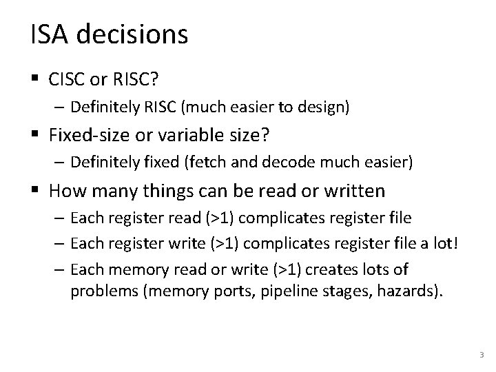
ISA decisions § CISC or RISC? – Definitely RISC (much easier to design) § Fixed-size or variable size? – Definitely fixed (fetch and decode much easier) § How many things can be read or written – Each register read (>1) complicates register file – Each register write (>1) complicates register file a lot! – Each memory read or write (>1) creates lots of problems (memory ports, pipeline stages, hazards). 3

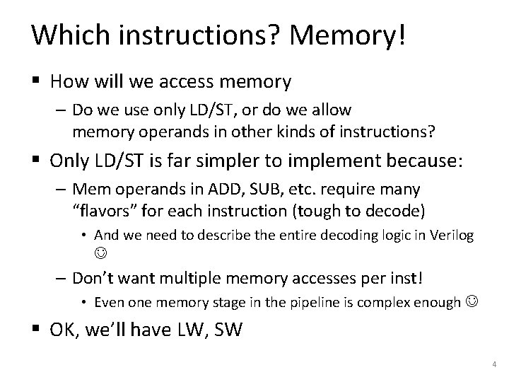
Which instructions? Memory! § How will we access memory – Do we use only LD/ST, or do we allow memory operands in other kinds of instructions? § Only LD/ST is far simpler to implement because: – Mem operands in ADD, SUB, etc. require many “flavors” for each instruction (tough to decode) • And we need to describe the entire decoding logic in Verilog – Don’t want multiple memory accesses per inst! • Even one memory stage in the pipeline is complex enough § OK, we’ll have LW, SW 4

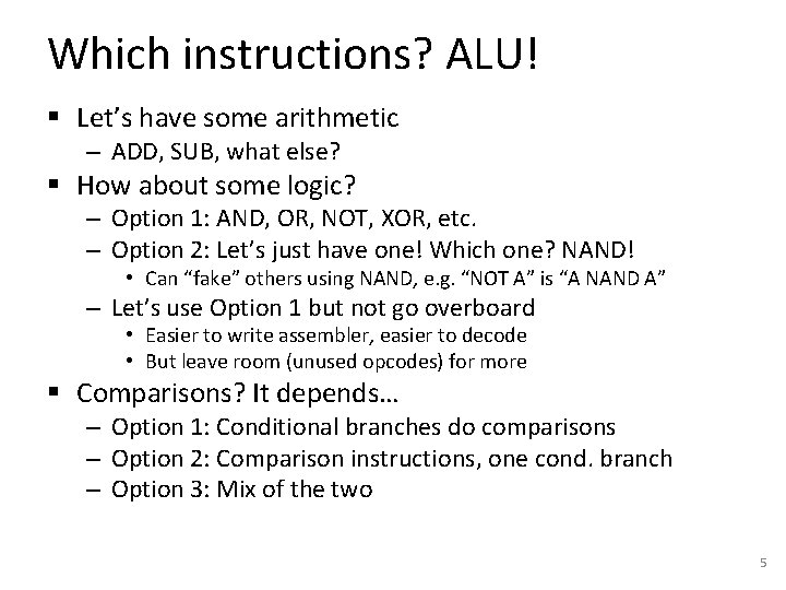
Which instructions? ALU! § Let’s have some arithmetic – ADD, SUB, what else? § How about some logic? – Option 1: AND, OR, NOT, XOR, etc. – Option 2: Let’s just have one! Which one? NAND! • Can “fake” others using NAND, e. g. “NOT A” is “A NAND A” – Let’s use Option 1 but not go overboard • Easier to write assembler, easier to decode • But leave room (unused opcodes) for more § Comparisons? It depends… – Option 1: Conditional branches do comparisons – Option 2: Comparison instructions, one cond. branch – Option 3: Mix of the two 5

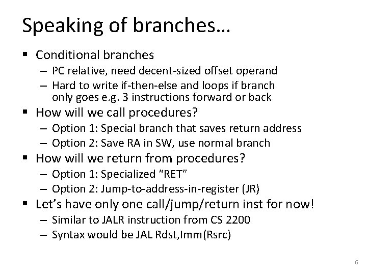
Speaking of branches… § Conditional branches – PC relative, need decent-sized offset operand – Hard to write if-then-else and loops if branch only goes e. g. 3 instructions forward or back § How will we call procedures? – Option 1: Special branch that saves return address – Option 2: Save RA in SW, use normal branch § How will we return from procedures? – Option 1: Specialized “RET” – Option 2: Jump-to-address-in-register (JR) § Let’s have only one call/jump/return inst for now! – Similar to JALR instruction from CS 2200 – Syntax would be JAL Rdst, Imm(Rsrc) 6

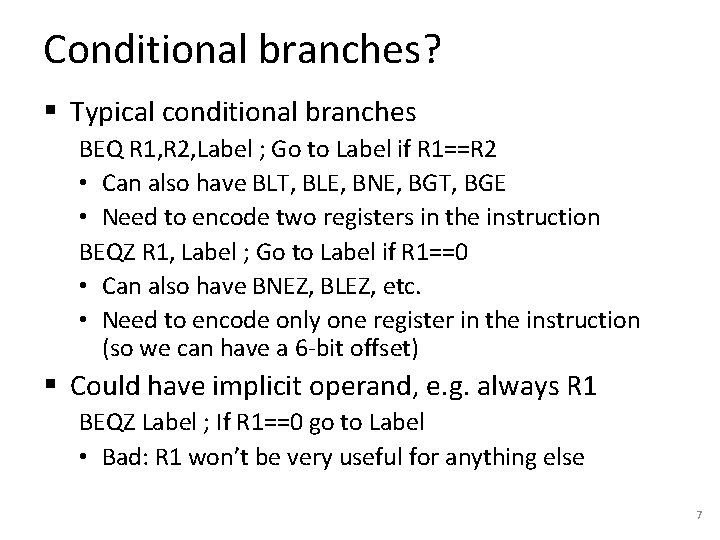
Conditional branches? § Typical conditional branches BEQ R 1, R 2, Label ; Go to Label if R 1==R 2 • Can also have BLT, BLE, BNE, BGT, BGE • Need to encode two registers in the instruction BEQZ R 1, Label ; Go to Label if R 1==0 • Can also have BNEZ, BLEZ, etc. • Need to encode only one register in the instruction (so we can have a 6 -bit offset) § Could have implicit operand, e. g. always R 1 BEQZ Label ; If R 1==0 go to Label • Bad: R 1 won’t be very useful for anything else 7

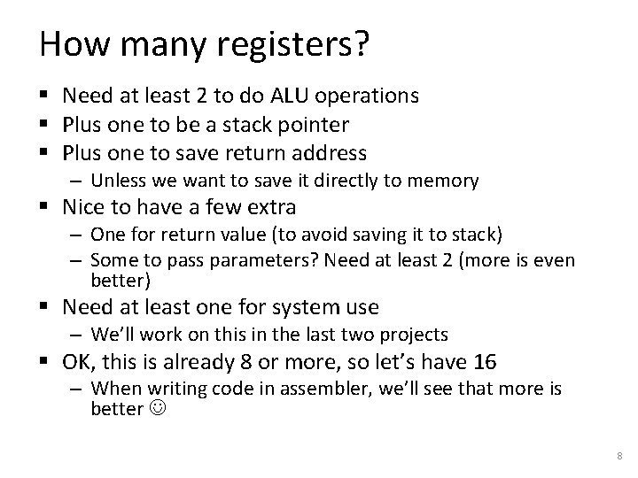
How many registers? § Need at least 2 to do ALU operations § Plus one to be a stack pointer § Plus one to save return address – Unless we want to save it directly to memory § Nice to have a few extra – One for return value (to avoid saving it to stack) – Some to pass parameters? Need at least 2 (more is even better) § Need at least one for system use – We’ll work on this in the last two projects § OK, this is already 8 or more, so let’s have 16 – When writing code in assembler, we’ll see that more is better 8

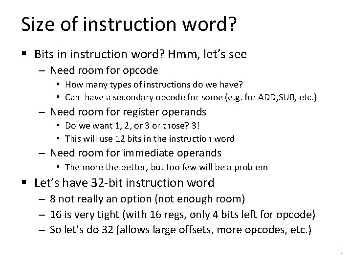
Size of instruction word? § Bits in instruction word? Hmm, let’s see – Need room for opcode • How many types of instructions do we have? • Can have a secondary opcode for some (e. g. for ADD, SUB, etc. ) – Need room for register operands • Do we want 1, 2, or 3 or those? 3! • This will use 12 bits in the instruction word – Need room for immediate operands • The more the better, but too few will be a problem § Let’s have 32 -bit instruction word – 8 not really an option (not enough room) – 16 is very tight (with 16 regs, only 4 bits left for opcode) – So let’s do 32 (allows large offsets, more opcodes, etc. ) 9

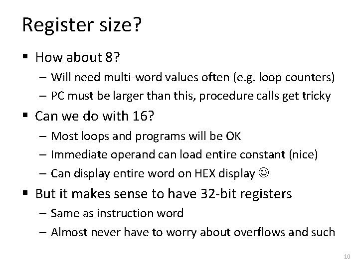
Register size? § How about 8? – Will need multi-word values often (e. g. loop counters) – PC must be larger than this, procedure calls get tricky § Can we do with 16? – Most loops and programs will be OK – Immediate operand can load entire constant (nice) – Can display entire word on HEX display § But it makes sense to have 32 -bit registers – Same as instruction word – Almost never have to worry about overflows and such 10

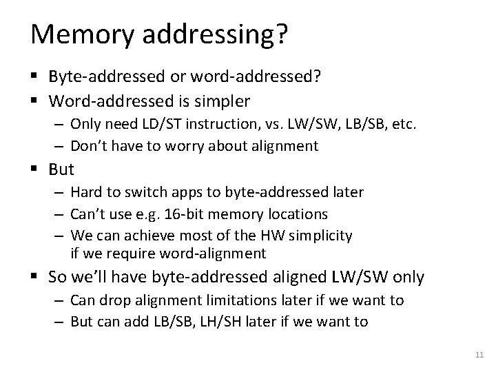
Memory addressing? § Byte-addressed or word-addressed? § Word-addressed is simpler – Only need LD/ST instruction, vs. LW/SW, LB/SB, etc. – Don’t have to worry about alignment § But – Hard to switch apps to byte-addressed later – Can’t use e. g. 16 -bit memory locations – We can achieve most of the HW simplicity if we require word-alignment § So we’ll have byte-addressed aligned LW/SW only – Can drop alignment limitations later if we want to – But can add LB/SB, LH/SH later if we want to 11

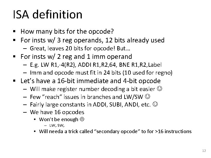
ISA definition § How many bits for the opcode? § For insts w/ 3 reg operands, 12 bits already used – Great, leaves 20 bits for opcode! But… § For insts w/ 2 reg and 1 imm operand – E. g. LW R 1, -4(R 2), ADDI R 1, R 2, 64, BNE R 1, R 2, Label – Imm and opcode must fit in 24 bits (10 used for regno) § Let’s have a 16 -bit immediate and 4 -bit opcode – – Will make register number decoding a bit easier Few “reach” issues in branches and LW/SW Fairly large constants in ADDI, SUBI, ANDI, etc. We have 16 opcodes • Won’t be enough – LW, SW, • Will needa a trick called “secondary opcode” to for >16 instructions 12
![Instruction Format Thus Far wire 3 0 op 1 Primary opcode wire 3 Instruction Format Thus Far wire [3: 0] op 1; // Primary opcode wire [3:](https://slidetodoc.com/presentation_image_h/8d90efa991e16576ddd298649b209a70/image-13.jpg)
Instruction Format Thus Far wire [3: 0] op 1; // Primary opcode wire [3: 0] rd, rs, rt; // Register operands wire [15: 0] imm; // 16 -bit immediate operand assign {op 1, rd, rs, rt, imm}=iword; § Decoding of register numbers is trivial § But… only 16 different instructions? – LW, SW (and leave room for LH, SH, LB, SB) – ADDI, ADD, SUB, AND, OR, XOR, NOT – BEQZ, BNEZ, JAL – This is already 16 • What if we want to add more later, e. g. MUL? 13

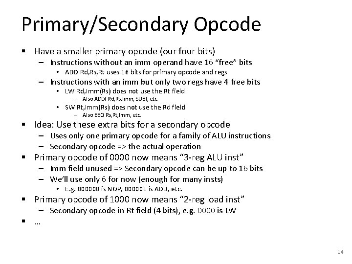
Primary/Secondary Opcode § Have a smaller primary opcode (our four bits) – Instructions without an imm operand have 16 “free” bits • ADD Rd, Rs, Rt uses 16 bits for primary opcode and regs – Instructions with an imm but only two regs have 4 free bits • LW Rd, Imm(Rs) does not use the Rt field – Also ADDI Rd, Rs, Imm, SUBI, etc. • SW Rt, Imm(Rs) does not use the Rd field – Also BEQ Rs, Rt, Imm, etc. § Idea: Use these extra bits for a secondary opcode – Uses only one primary opcode for a family of ALU instructions – Secondary opcode => the actual operation § Primary opcode of 0000 now means “ 3 -reg ALU inst” – Imm field unused => Secondary opcode can be up to 16 bits – We’ll use only 6 for now (enough for many insts) • E. g. 000000 is NOP, 000001 is ADD, etc. § Primary opcode of 1000 now means “ 2 -reg load inst” – Secondary opcode in Rt field (4 bits), e. g. 0000 is LW § … 14

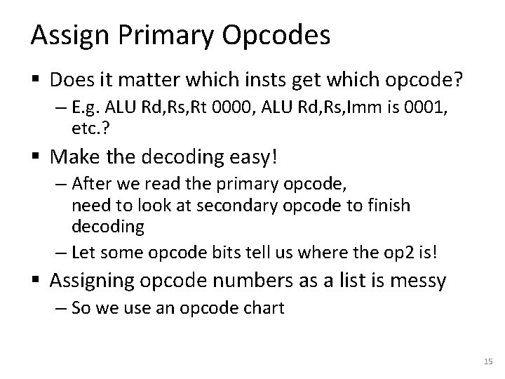
Assign Primary Opcodes § Does it matter which insts get which opcode? – E. g. ALU Rd, Rs, Rt 0000, ALU Rd, Rs, Imm is 0001, etc. ? § Make the decoding easy! – After we read the primary opcode, need to look at secondary opcode to finish decoding – Let some opcode bits tell us where the op 2 is! § Assigning opcode numbers as a list is messy – So we use an opcode chart 15

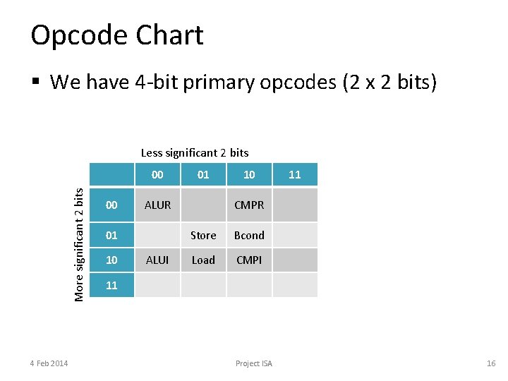
Opcode Chart § We have 4 -bit primary opcodes (2 x 2 bits) Less significant 2 bits More significant 2 bits 00 4 Feb 2014 00 ALUR 01 10 01 ALUI 10 11 CMPR Store Bcond Load CMPI 11 Project ISA 16

Load (op 1=1001) Opcode Chart § We have a 4 -bit secondary opcode instead of Rt More significant 2 bits Less significant 2 bits 00 00 01 10 LW LH LB 11 Will add these later 01 10 Why not here? 11 No particular reason! 18

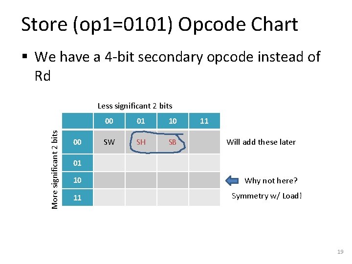
Store (op 1=0101) Opcode Chart § We have a 4 -bit secondary opcode instead of Rd More significant 2 bits Less significant 2 bits 00 00 01 10 SW SH SB 11 Will add these later 01 10 11 Why not here? Symmetry w/ Load! 19

ALUR (op 1=0000) Opcode Chart § 16 -bit secondary opcode instead of Imm – We’ll keep bits 11: 4 at zero, use only [3: 0]. Why? More significant 2 bits Less significant 2 bits 00 01 10 00 ADD SUB 01 AND OR XOR NAND NOR NXOR 11 10 11 20

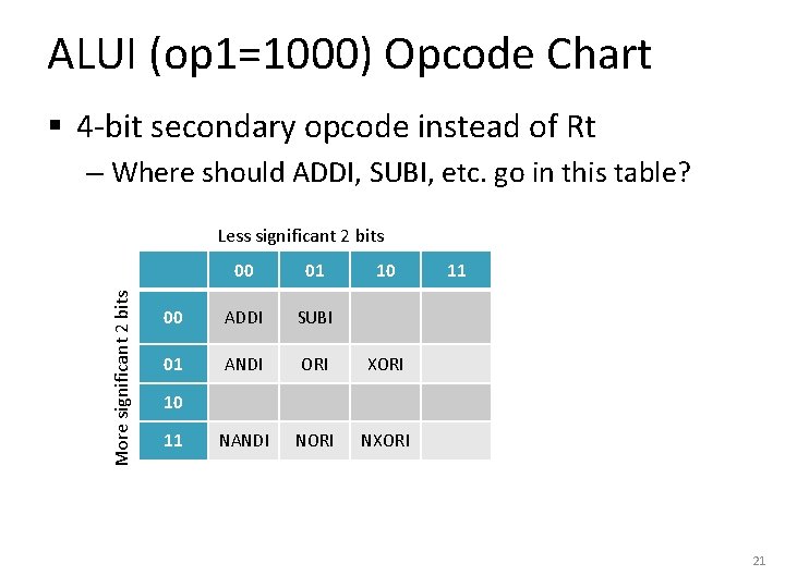
ALUI (op 1=1000) Opcode Chart § 4 -bit secondary opcode instead of Rt – Where should ADDI, SUBI, etc. go in this table? More significant 2 bits Less significant 2 bits 00 01 10 00 ADDI SUBI 01 ANDI ORI XORI NANDI NORI NXORI 11 10 11 21

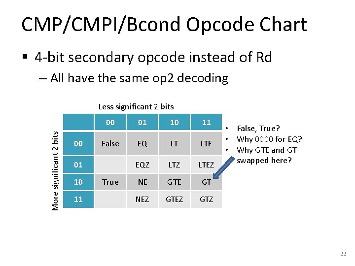
CMP/CMPI/Bcond Opcode Chart § 4 -bit secondary opcode instead of Rd – All have the same op 2 decoding More significant 2 bits Less significant 2 bits 00 00 01 10 11 False EQ LT LTE EQZ LTEZ NE GT NEZ GTZ 01 10 11 True • False, True? • Why 0000 for EQ? • Why GTE and GT swapped here? 22

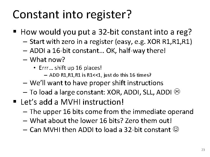
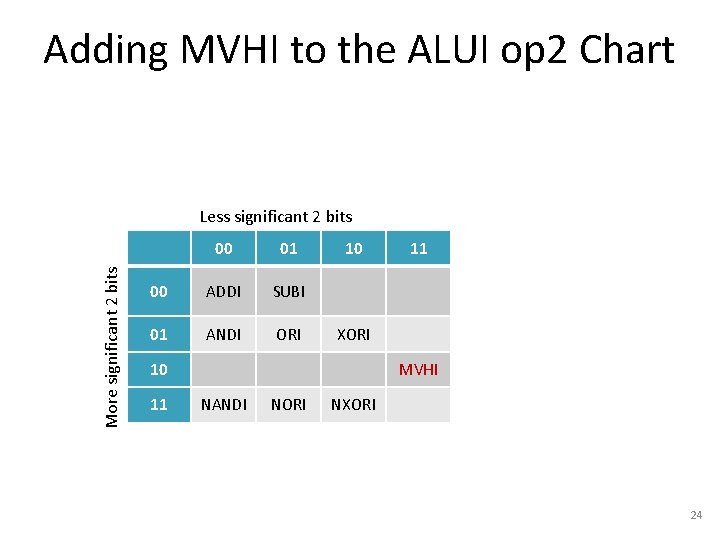
Constant into register? § How would you put a 32 -bit constant into a reg? – Start with zero in a register (easy, e. g. XOR R 1, R 1) – ADDI a 16 -bit constant… OK, half-way there! – What now? • Errr… shift up 16 places! – ADD R 1, R 1 is R 1<<1, just do this 16 times? – We’ll want to have proper shift instructions – To load a large constant: XOR, ADDI, SLL, ADDI § Let’s add a MVHI instruction! – The upper 16 bits come from the immediate operand – What about the lower 16 bits? Zero them out! – Can MVHI then ADDI to load a 32 -bit constant 23

Adding MVHI to the ALUI op 2 Chart More significant 2 bits Less significant 2 bits 00 01 00 ADDI SUBI 01 ANDI ORI 10 XORI 10 11 11 MVHI NANDI NORI NXORI 24

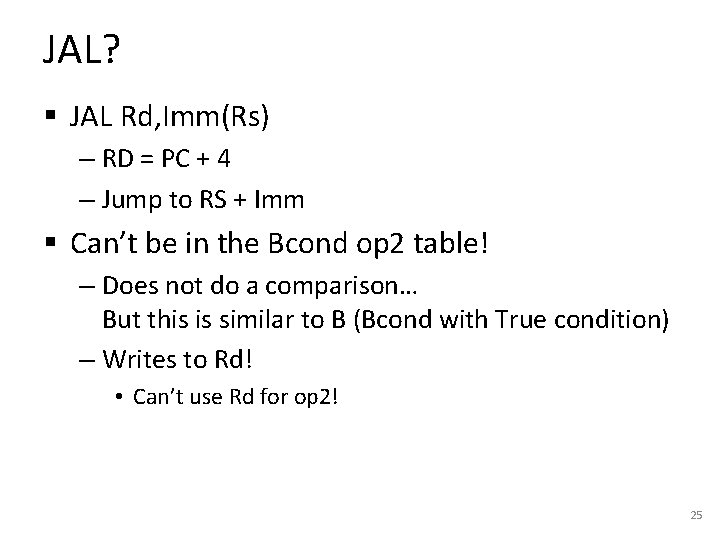
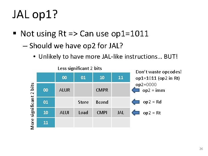
JAL? § JAL Rd, Imm(Rs) – RD = PC + 4 – Jump to RS + Imm § Can’t be in the Bcond op 2 table! – Does not do a comparison… But this is similar to B (Bcond with True condition) – Writes to Rd! • Can’t use Rd for op 2! 25

JAL op 1? § Not using Rt => Can use op 1=1011 – Should we have op 2 for JAL? • Unlikely to have more JAL-like instructions… BUT! Less significant 2 bits More significant 2 bits 00 00 ALUR 01 10 01 ALUI 10 11 CMPR Store Bcond Load CMPI Don’t waste opcodes! op 1=1011 (op 2 in Rt) op 2=0000 op 2 = imm op 2 = Rd JAL op 2 = Rt 11 26

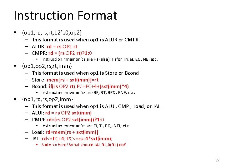
Instruction Format § {op 1, rd, rs, rt, 12’b 0, op 2} – This format is used when op 1 is ALUR or CMPR – ALUR: rd = rs OP 2 rt – CMPR: rd = (rs OP 2 rt)? 1: 0 • Instruction mnemonics are F (False), T (for True), EQ, NE, etc. § {op 1, op 2, rs, rt, imm} – This format is used when op 1 is Store or Bcond – Store: mem[rs + sxt(imm)]=rt – Bcond: if(rs OP 2 rt) PC=PC+4+(sxt(imm)*4) • Instruction mnemonics are BF, BT, BEQ, BNE, etc. § {op 1, rd, rs, op 2, imm} – This format is used when op 1 is ALUI, CMPI, Load, or JAL – ALUI: rd = rs OP 2 sxt(imm) – CMPI: rd=(rs OP 2 sxt(imm))? 1: 0 • Instruction mnemonics are FI, TI, EQI, NEI, etc. – Load: rd=mem[rs + sxt(imm)] – JAL: rd<=PC+4; PC<=rs+4*sxt(imm); • Note <= here! What should JAL R 1, 0(R 1) do? 27

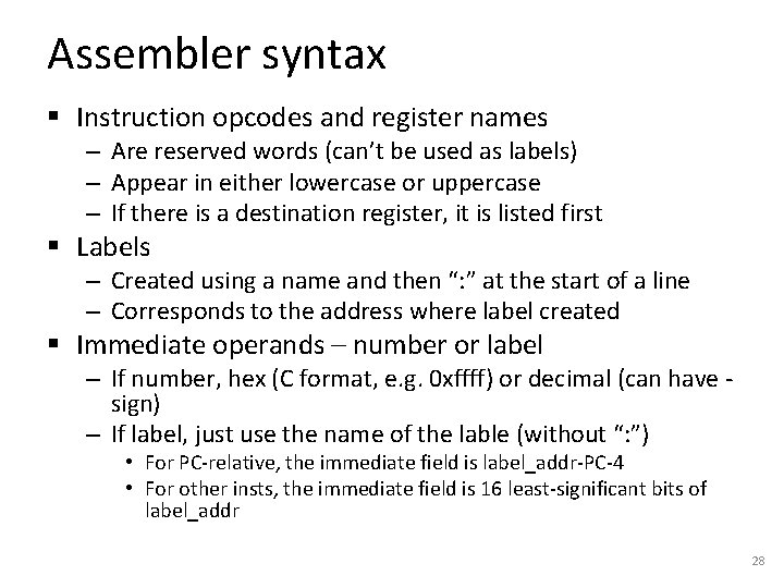
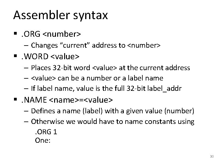
Assembler syntax § Instruction opcodes and register names – Are reserved words (can’t be used as labels) – Appear in either lowercase or uppercase – If there is a destination register, it is listed first § Labels – Created using a name and then “: ” at the start of a line – Corresponds to the address where label created § Immediate operands – number or label – If number, hex (C format, e. g. 0 xffff) or decimal (can have sign) – If label, just use the name of the lable (without “: ”) • For PC-relative, the immediate field is label_addr-PC-4 • For other insts, the immediate field is 16 least-significant bits of label_addr 28

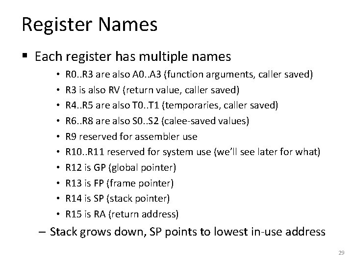
Register Names § Each register has multiple names • • • R 0. . R 3 are also A 0. . A 3 (function arguments, caller saved) R 3 is also RV (return value, caller saved) R 4. . R 5 are also T 0. . T 1 (temporaries, caller saved) R 6. . R 8 are also S 0. . S 2 (calee-saved values) R 9 reserved for assembler use R 10. . R 11 reserved for system use (we’ll see later for what) R 12 is GP (global pointer) R 13 is FP (frame pointer) R 14 is SP (stack pointer) R 15 is RA (return address) – Stack grows down, SP points to lowest in-use address 29

Assembler syntax §. ORG <number> – Changes “current” address to <number> §. WORD <value> – Places 32 -bit word <value> at the current address – <value> can be a number or a label name – If label name, value is the full 32 -bit label_addr §. NAME <name>=<value> – Defines a name (label) with a given value (number) – Otherwise we would have to name constants using. ORG 1 One: 30

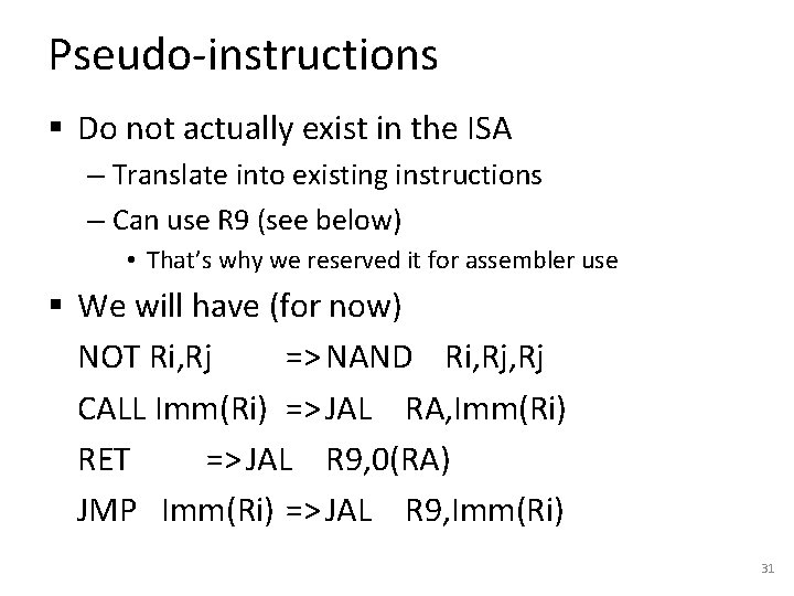
Pseudo-instructions § Do not actually exist in the ISA – Translate into existing instructions – Can use R 9 (see below) • That’s why we reserved it for assembler use § We will have (for now) NOT Ri, Rj => NAND Ri, Rj CALL Imm(Ri) => JAL RA, Imm(Ri) RET => JAL R 9, 0(RA) JMP Imm(Ri) => JAL R 9, Imm(Ri) 31

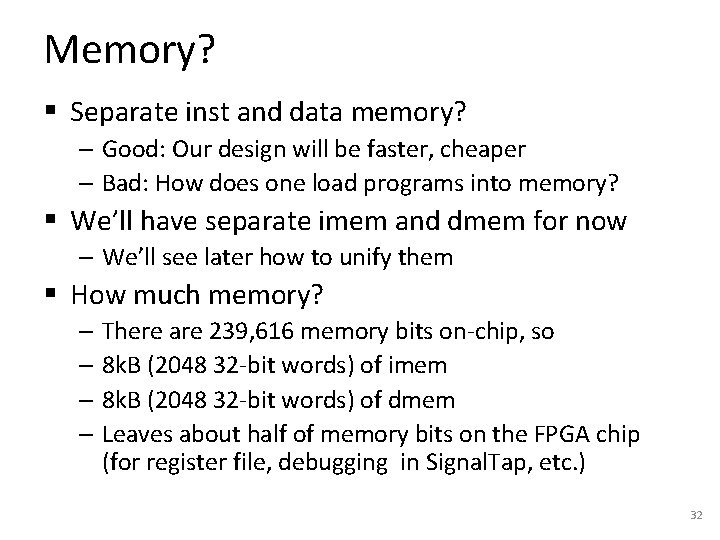
Memory? § Separate inst and data memory? – Good: Our design will be faster, cheaper – Bad: How does one load programs into memory? § We’ll have separate imem and dmem for now – We’ll see later how to unify them § How much memory? – There are 239, 616 memory bits on-chip, so – 8 k. B (2048 32 -bit words) of imem – 8 k. B (2048 32 -bit words) of dmem – Leaves about half of memory bits on the FPGA chip (for register file, debugging in Signal. Tap, etc. ) 32

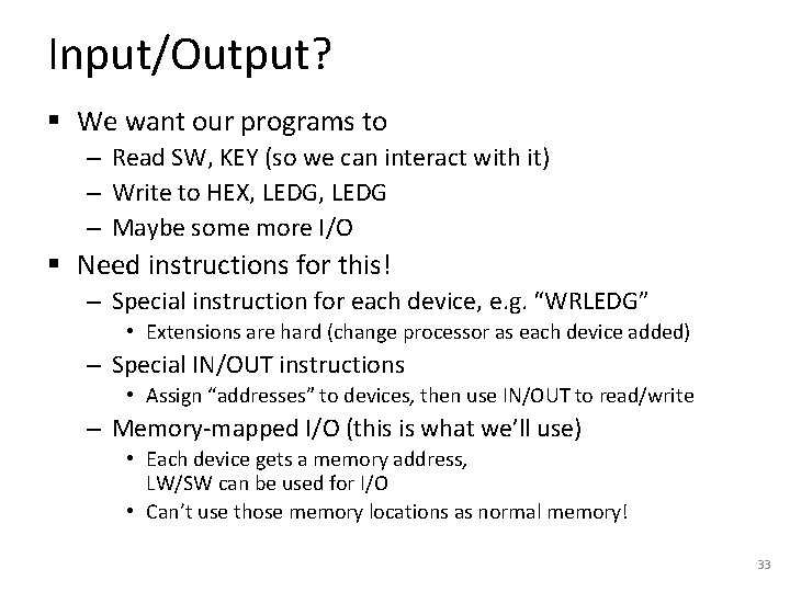
Input/Output? § We want our programs to – Read SW, KEY (so we can interact with it) – Write to HEX, LEDG – Maybe some more I/O § Need instructions for this! – Special instruction for each device, e. g. “WRLEDG” • Extensions are hard (change processor as each device added) – Special IN/OUT instructions • Assign “addresses” to devices, then use IN/OUT to read/write – Memory-mapped I/O (this is what we’ll use) • Each device gets a memory address, LW/SW can be used for I/O • Can’t use those memory locations as normal memory! 33

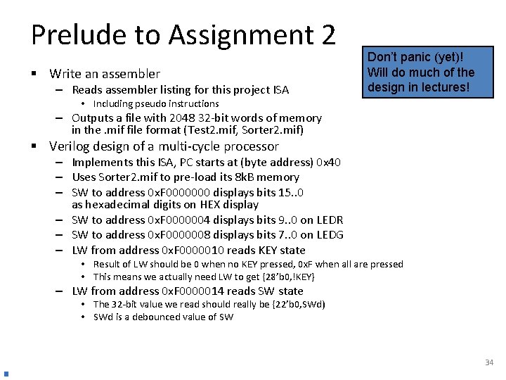
Prelude to Assignment 2 § Write an assembler – Reads assembler listing for this project ISA Don’t panic (yet)! Will do much of the design in lectures! • Including pseudo instructions – Outputs a file with 2048 32 -bit words of memory in the. mif file format (Test 2. mif, Sorter 2. mif) § Verilog design of a multi-cycle processor – Implements this ISA, PC starts at (byte address) 0 x 40 – Uses Sorter 2. mif to pre-load its 8 k. B memory – SW to address 0 x. F 0000000 displays bits 15. . 0 as hexadecimal digits on HEX display – SW to address 0 x. F 0000004 displays bits 9. . 0 on LEDR – SW to address 0 x. F 0000008 displays bits 7. . 0 on LEDG – LW from address 0 x. F 0000010 reads KEY state • Result of LW should be 0 when no KEY pressed, 0 x. F when all are pressed • This means we actually need LW to get {28’b 0, !KEY} – LW from address 0 x. F 0000014 reads SW state • The 32 -bit value we read should really be {22’b 0, SWd) • SWd is a debounced value of SW 34