IRVISUVXgammaTe V detectors and readout electronics 10 2
- Slides: 21

IR/VIS/UV/X/gamma/Te. V detectors and readout electronics 10 -2 ÷ 1012 e. V Claudio Labanti, Giovanni Bonanno, Favio Bortoletto, Ezio Caroli, Rosario Cosentino, Ettore Del Monte, Marco Feroci, Giovanni La Rosa, Claudio Macculi, Michela Uslenghi Napoli 27 -28. 3. 2019

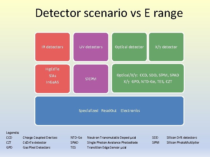
Detector scenario vs E range IR detectors UV detectors Hg. Cd. Te Si. As In. Ga. AS Si. CPM Optical detector X/ detector Optical/X/ : CCD, SDD, Si. PM, SPAD X/ GPD, NTD-Ge, TES, CZT Specialized Read. Out Electronics Legenda: CCD CZT GPD Charge Coupled Devices Cd. Zn. Te detector Gas Pixel Detectors NTD-Ge SPAD TES Neutron Transmutatio Doped µcal Single Photon Avalance Photodiode Transition Edge Sensor µcal SDD Si. PM Silicon Drft detectors Silicon Photo. Multiplier

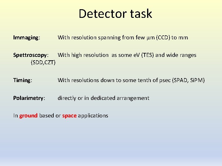
Detector task Immaging: With resolution spanning from few µm (CCD) to mm Spettroscopy: With high resolution as some e. V (TES) and wide ranges (SDD, CZT) Timing: With resolutions down to some tenth of psec (SPAD, Si. PM) Polarimetry: directly or in dedicated arrangement In ground based or space applications

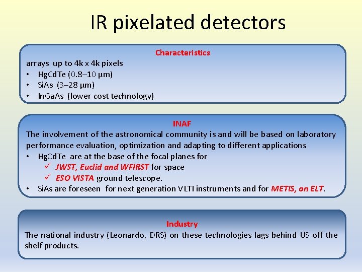
IR pixelated detectors arrays up to 4 k x 4 k pixels • Hg. Cd. Te (0. 8– 10 μm) • Si. As (3– 28 μm) • In. Ga. As (lower cost technology) Characteristics INAF The involvement of the astronomical community is and will be based on laboratory performance evaluation, optimization and adapting to different applications • Hg. Cd. Te are at the base of the focal planes for ü JWST, Euclid and WFIRST for space ü ESO VISTA ground telescope. • Si. As are foreseen for next generation VLTI instruments and for METIS, on ELT. Industry The national industry (Leonardo, DRS) on these technologies lags behind US off the shelf products.

Silicon Carbide Photo Multiplier (Si. CPM) for UV solar blind application Characteristics 4 H-Si. C based photodiodes are suitable choice for UV astronomy owing to their high intrinsic visible blindness INAF Si. C-APD technology developed at CNR-IMM, in collaboration with INAF and ST Microelectronics succeeded in obtaining. The next step will be the realization of a Si. C-SPAD (technology that allows to operate a Si. C-APD in Geiger mode) using quenching resistors and finally assembling many Si. C -SPAD in parallel to obtain Si. CPMs. Industry Collaboration with ST Microelectronics.

Optical detectors Characteristics State of the art CCD offers the possibility of large mosaics of CCD in the extended range of high QE (400 -800 nm) and low dark noise (4 e-/pix/hour) CMOS are optimal for short-time exposure applications (fast imaging, adaptive optics, space applications). INAF CCD or CMOS detectors are used in all the ground telescopes and several space missions. While the detectors are made by the industry, the development of the front-end electronics, the detector controller, the test and the characterization are carried out in the INAF institutes.

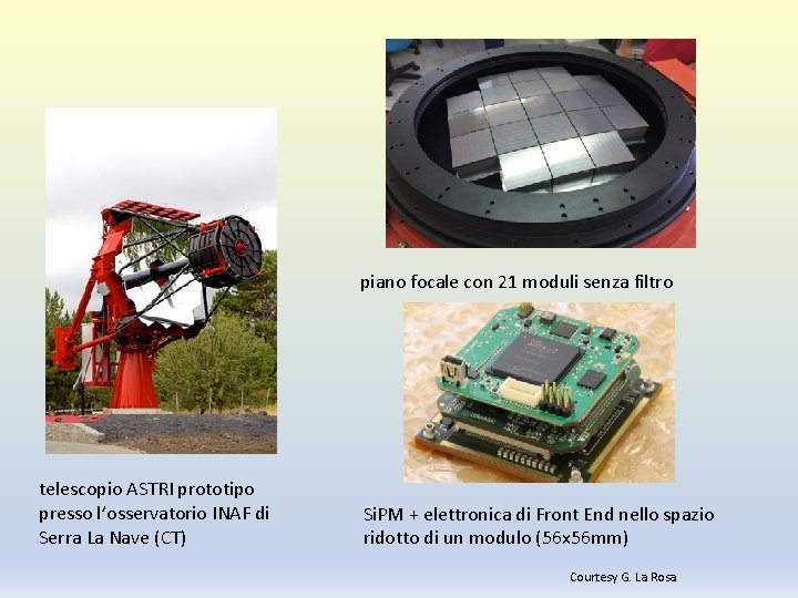
Silicon Photomultiplier (Si. PM) Characteristics Alternative to PMTs in almost all astronomy applications SDD operate in a limited Geiger mode, in order to achieve a gain at the level of 106 high QE, fast response. INAF The Si. PM are studied in INAF, as focal plane sensors of the Imaging Atmospheric Cherenkov Telescope (IACT) and for ASTRI SST-2 M a Cherenkov telescope prototype proposed by INAF as Small Sized Telescope (SST) for the Cherenkov Telescope Array (CTA) observatory. Industry Two Italian industries offer state-of-the-art Si. PM: ü Advan. Si. D ü ST Microelectronics

piano focale con 21 moduli senza filtro telescopio ASTRI prototipo presso l’osservatorio INAF di Serra La Nave (CT) Si. PM + elettronica di Front End nello spazio ridotto di un modulo (56 x 56 mm) Courtesy G. La Rosa

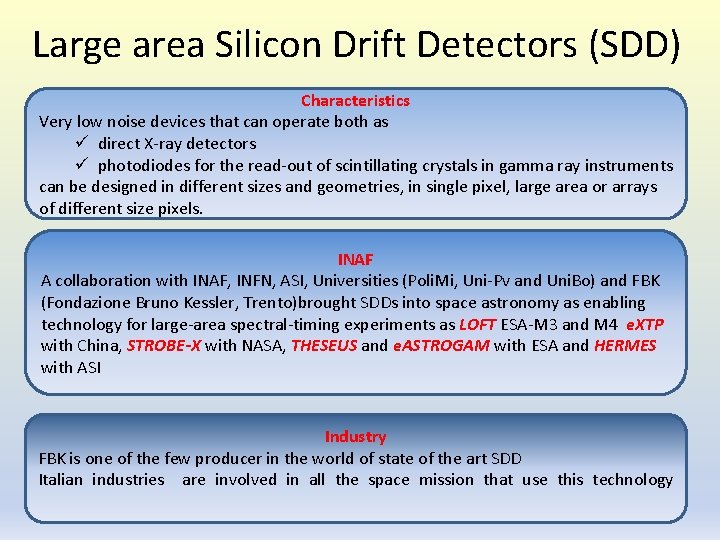
Large area Silicon Drift Detectors (SDD) Characteristics Very low noise devices that can operate both as ü direct X-ray detectors ü photodiodes for the read-out of scintillating crystals in gamma ray instruments can be designed in different sizes and geometries, in single pixel, large area or arrays of different size pixels. INAF A collaboration with INAF, INFN, ASI, Universities (Poli. Mi, Uni-Pv and Uni. Bo) and FBK (Fondazione Bruno Kessler, Trento)brought SDDs into space astronomy as enabling technology for large-area spectral-timing experiments as LOFT ESA-M 3 and M 4 e. XTP with China, STROBE-X with NASA, THESEUS and e. ASTROGAM with ESA and HERMES with ASI Industry FBK is one of the few producer in the world of state of the art SDD Italian industries are involved in all the space mission that use this technology

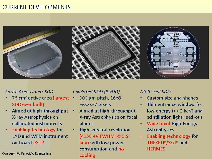
CURRENT DEVELOPMENTS Large Area Linear SDD • 76 cm 2 active area (largest SDD ever built) • Aimed at high-throughput X-ray Astrophysics on collimated instruments • Enabling technology for LAD and WFM instrument on-board e. XTP Courtesy M. Feroci, Y. Evangelista Pixelated SDD (Pix. DD) • 300 μm pitch, 16 x 8 → 32 x 32 pixels • Aimed at high-throughput X-ray Astrophysics on focal planes • High spectral resolution (<150 e. V FWHM @ 5. 9 ke. V) with low power consumption and no cooling Multi-cell SDD • Custom size and shapes • Thin entrance window for low energy (<< 2 ke. V) and scintillation light read-out • Wide band High Energy Astrophysics • Enabling technology for THESEUS/XGIS and HERMES

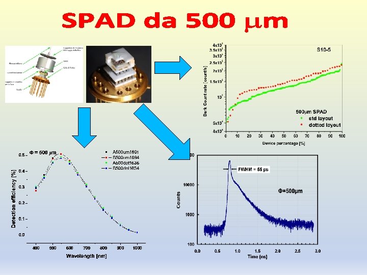
Single Photon Avalanche Diode (SPAD) Characteristics SPAD feature single photon detection efficiency, a timing accuracy as good as 40 ps, although with no spectroscopic capabilities Detector range from 50 μm and up to 500 μm diameter INAF SPAD are developed at Politecnico di Milano and manufactured at IMM-CNR. Their application in astronomy both naked than coupled to scintillating-fibers are studied within INAF and ASI funded technological projects Industry Micro Photon Device a PMI from Bz develops and produce photon counting devices based SPAD.


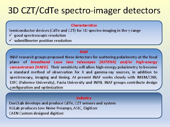
3 D CZT/Cd. Te spectro-imager detectors Characteristics Semiconductor devices (Cd. Te and CZT) for 3 D spectro-imaging in the range ü good spectroscopic resolution ü submillimeter position resolution INAF research groups proposed these detectors for scattering polarimetry at the focal plane of broadband Laue lens telescopes (ASTENA) and/or high-energy concentrators (HAED). Their sensitivity will allow high-energy polarimetry to become a standard method of observation for X and gamma-ray sources, in addition to spectroscopy, imaging and timing. At present INAF works closely with IMEM/CNR, DIFC (Palermo University), Pavia University and INFN. INAF groups contribute design configuration and optimization Industry Due 2 Lab develops and produce Cd. Te, CZT sensors and system XGLab produces Low Noise Preamps, ASIC, Digitizer CAEN Custom designed digitizer

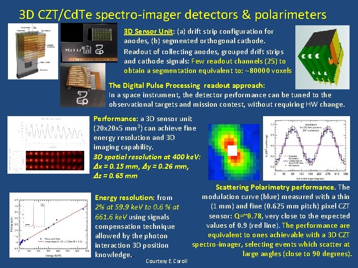
3 D CZT/Cd. Te spectro-imager detectors & polarimeters 3 D Sensor Unit: (a) drift strip configuration for anodes, (b) segmented orthogonal cathode. Readout of collecting anodes, grouped drift strips and cathode signals: Few readout channels (25) to obtain a segmentation equivalent to: 80000 voxels The Digital Pulse Processing readout approach: In a space instrument, the detector performance can be tuned to the observational targets and mission contest, without requiring HW change. Performance: a 3 D sensor unit (20 x 5 mm 3) can achieve fine energy resolution and 3 D imaging capability. 3 D spatial resolution at 400 ke. V: x = 0. 15 mm, y = 0. 26 mm, z = 0. 65 mm Energy resolution: from 2% at 59. 9 ke. V to 0. 6 % at 661. 6 ke. V using signals compensation technique allowed by the photon interaction 3 D position knowledge. . Courtesy E. Caroli Scattering Polarimetry performance. The modulation curve (blue) measured with a thin (1 mm) and fine (0. 625 mm pitch) pixel CZT sensor: Q=~0. 78, very close to the expected values of 0. 9 (red line). The performance are equivalent to ones achievable with a 3 D CZT spectro-imager, selecting events which scatter at large angles (close to 90 degrees).

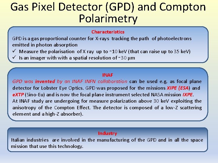
Gas Pixel Detector (GPD) and Compton Polarimetry Characteristics GPD is a gas proportional counter for X-rays tracking the path of photoelectrons emitted in photon absorption ü Measure the polarisation of X ray up to ∼ 10 ke. V (that can raise up to 35 ke. V) ü Is an imager with a spatial resolution of ∼ 30 μm INAF GPD was invented by an INAF INFN collaboration can be used e. g. as focal plane detector for Lobster Eye Optics. GPD was proposed for the missions XIPE (ESA) and e. XTP (Sino-Eu) and is now the focal plane instrument selected NASA mission IXPE. At INAF study are undergoing for measure polarization above 30 ke. V exploiting the anisotropy of the Compton Effect. The detector is composed of a low-Z scattering element and a high-Z absorber). Industry Italian industries are involved in the manufacturing of the GPD and in all the space mission that use this technology.

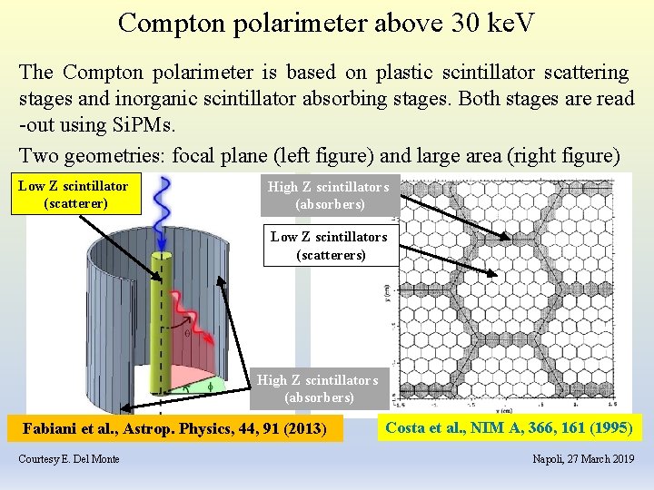
Compton polarimeter above 30 ke. V The Compton polarimeter is based on plastic scintillator scattering stages and inorganic scintillator absorbing stages. Both stages are read -out using Si. PMs. Two geometries: focal plane (left figure) and large area (right figure) Low Z scintillator (scatterer) High Z scintillators (absorbers) Low Z scintillators (scatterers) High Z scintillators (absorbers) Fabiani et al. , Astrop. Physics, 44, 91 (2013) Courtesy E. Del Monte Costa et al. , NIM A, 366, 161 (1995) Napoli, 27 March 2019

Neutron Transmutation Doped NTD Germanium X-Ray microcalorimeters Characteristics Excellent energy resolution Single, cryogenic semiconductor micro-machined microcalorimeters with NTD Ge thermistors have widely and successfully been adopted from infrared to soft-gamma rays. Usable in a wide range of temperature, with a wide dynamic energy range with a read -out electronics based on low noise, low cost, commercially available components. INAF is developing a planar process to build scalable arrays, optimize the performance for X-ray detection, and increase the count rate.

Transition Edge Sensor TES Microcalorimeter detectors and Cryogenics Characteristics Excellent energy resolution. The technology deal with microcalorimeter made of normal-metal, semiconductors and superconductors cooled at 0. 1 K, and the readout electronics (cold based on SQu. ID, and warm electronics) INAF The main scientific driver is related to the ATHENA ESA mission. In the frame of an INAF- INFN collaboration and inside an international consortium that will build the TES-based X-IFU instrument on board ATHENA. INAF has the responsibility of Cryogenic Anti-Coincidence detector (Cryo. AC) of X-IFU Industry The Cryo. AC will be fully developed in Italy. The spin-off towards the Italian industries is robust and concern ü TAS-I (electronics) ü CGS/FBK (electronics and structural issues)

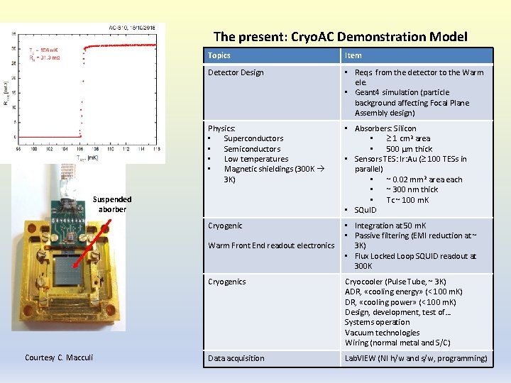
The present: Cryo. AC Demonstration Model Topics Item Detector Design • Reqs. from the detector to the Warm ele. • Geant 4 simulation (particle background affecting Focal Plane Assembly design) Physics: • Superconductors • Semiconductors • Low temperatures • Magnetic shieldings (300 K 3 K) • Absorbers: Silicon • 1 cm 2 area • 500 µm thick • Sensors TES: Ir: Au ( 100 TESs in parallel) • ~ 0. 02 mm 2 area each • ~ 300 nm thick • Tc ~ 100 m. K • SQu. ID Cryogenic • Integration at 50 m. K • Passive filtering (EMI reduction at ~ 3 K) • Flux Locked Loop SQUID readout at 300 K Suspended aborber Warm Front End readout electronics Courtesy C. Macculi Cryogenics Cryocooler (Pulse Tube, ~ 3 K) ADR, «cooling energy» (< 100 m. K) DR, «cooling power» (< 100 m. K) Design, development, test of… Systems operation Vacuum technologies Wiring (normal metal and S/C) Data acquisition Lab. VIEW (NI h/w and s/w, programming)

Read-out electronics Scenario Special instruments require special electronics developed inside INAF laboratories. This is particularly true for electronics that involve Application Specific Integrated Circuits (ASIC) or programmable logic, like Field Programmable Gate Array (FPGA). INAF scientists drive the design and development of ASICs and FPGA firmware in order to satisfy the scientific requirements also in collaboration with Universities and INFN. Industry The industry enters mainly at the engineering phase, for satellites or ground telescopes. The development of specific electronics thus requires that the expertise is maintained in the INAF laboratories, working in synergy with industries.

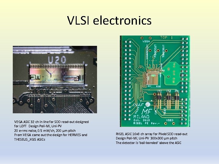
VLSI electronics VEGA ASIC 32 ch in line for SDD read-out designed for LOFT Design Poli-Mi, Uni-PV 20 e-rms noise, 0. 5 m. W/ch, 200 µm pitch From VEGA came out the design for HERMES and THESEUS_XGIS ASICs RIGEL ASIC 16 x 8 ch array for Pixdd SDD read-out Design Poli-Mi, Uni-PV 300 x 300 µm pitch The detector is ‘ball-bonded’ above the ASIC