IPC Part 2 Electronic Design and CADCAM A








- Slides: 66

IPC Part: 2 Electronic Design and CAD/CAM A circuit board is born and takes its first tottering steps.


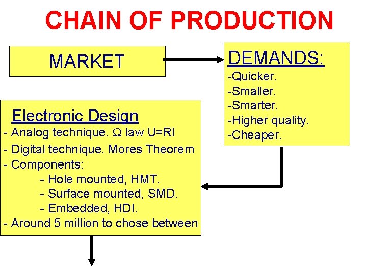
CHAIN OF PRODUCTION MARKET Electronic Design - Analog technique. law U=RI - Digital technique. Mores Theorem - Components: - Hole mounted, HMT. - Surface mounted, SMD. - Embedded, HDI. - Around 5 million to chose between DEMANDS: -Quicker. -Smaller. -Smarter. -Higher quality. -Cheaper.

I like complicated functions on a small surface!! The Electronic Designer

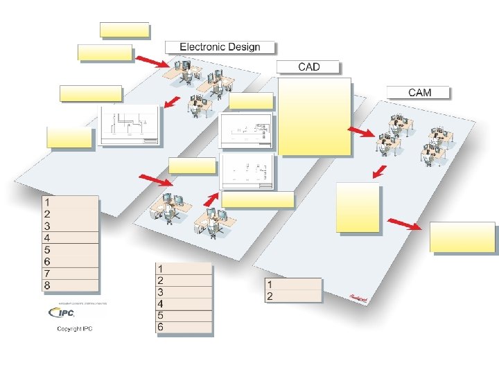
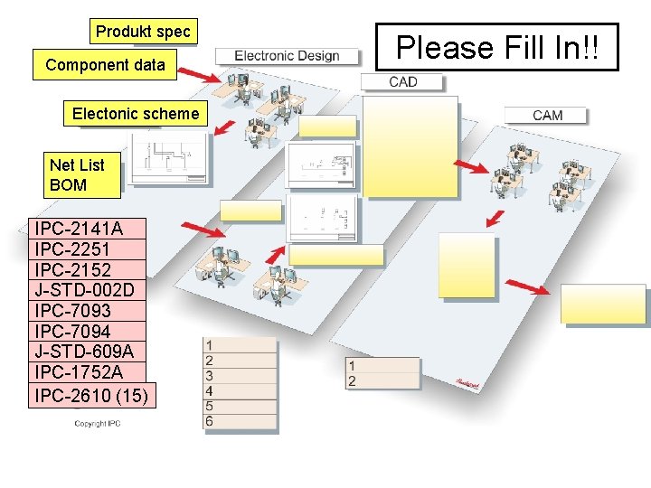
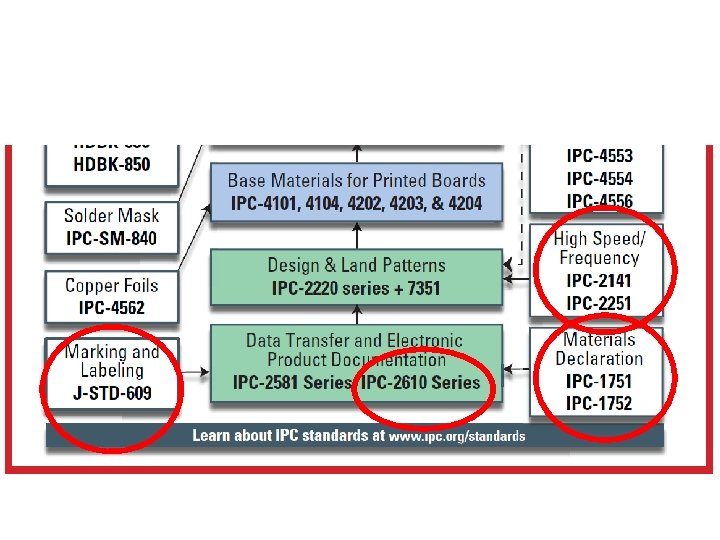
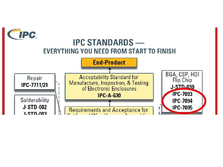
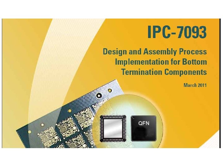
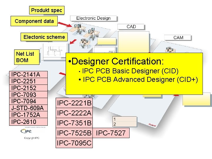
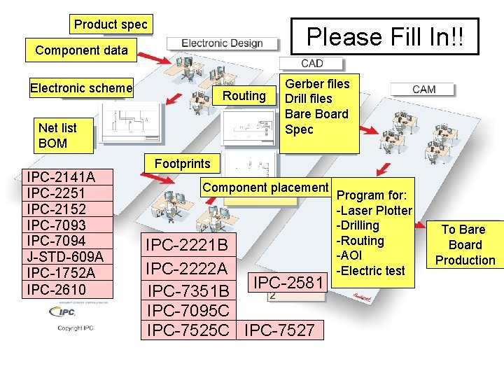
Produkt spec Component data Electonic scheme Net List BOM IPC-2141 A IPC-2251 IPC-2152 J-STD-002 D IPC-7093 IPC-7094 J-STD-609 A IPC-1752 A IPC-2610 (15) Please Fill In!!


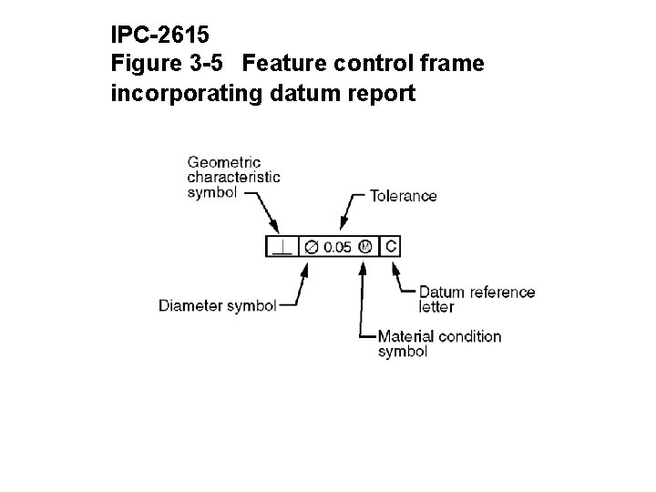
IPC-2615 Figure 3 -5 Feature control frame incorporating datum report

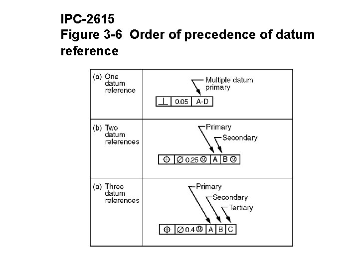
IPC-2615 Figure 3 -6 Order of precedence of datum reference


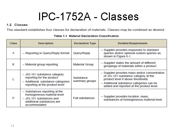
IPC-1752 A - Classes 14

Joint Industry Guide


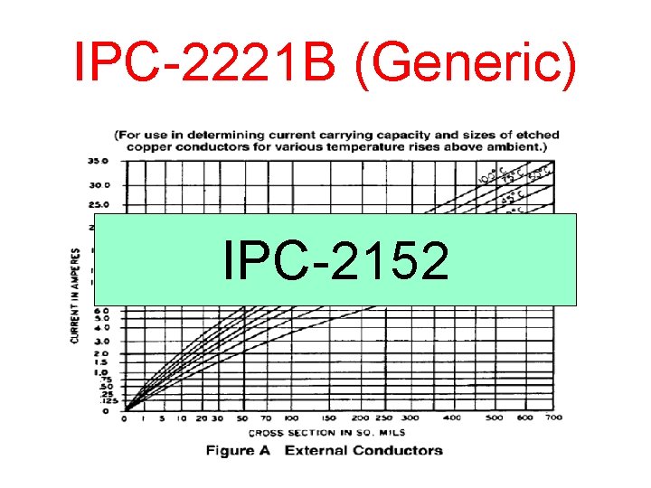
IPC-2221 B (Generic) IPC-2152


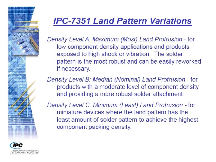
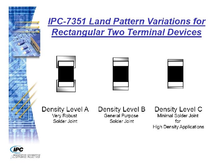
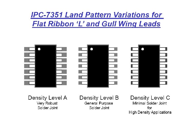
What is IPC-7351 B? My footprints hasn't changed since 1903! The CAD People

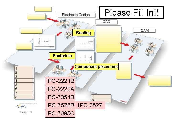
Please Fill In!! Routing Footprints Component placement IPC-2221 B IPC-2222 A IPC-7351 B IPC-7525 B IPC-7527 IPC-7095 C


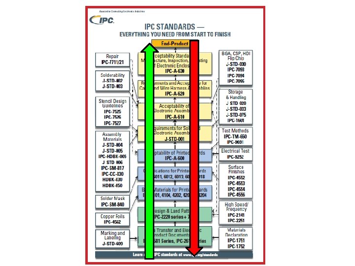
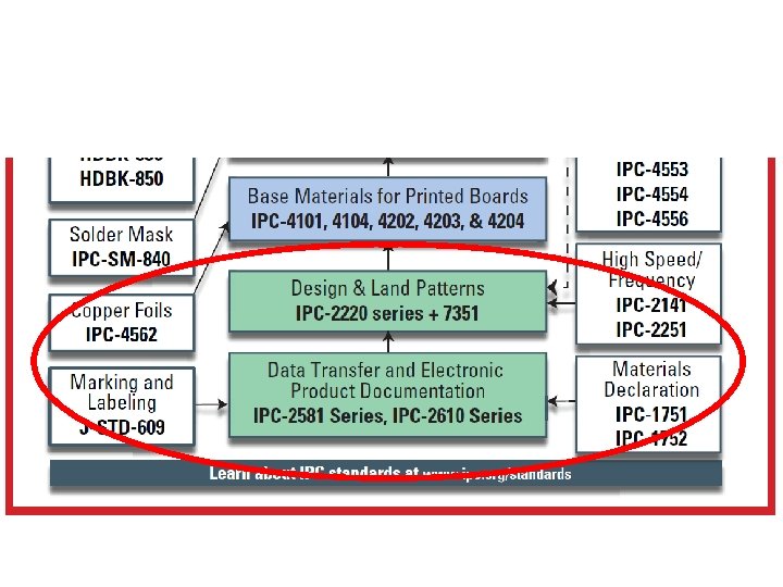
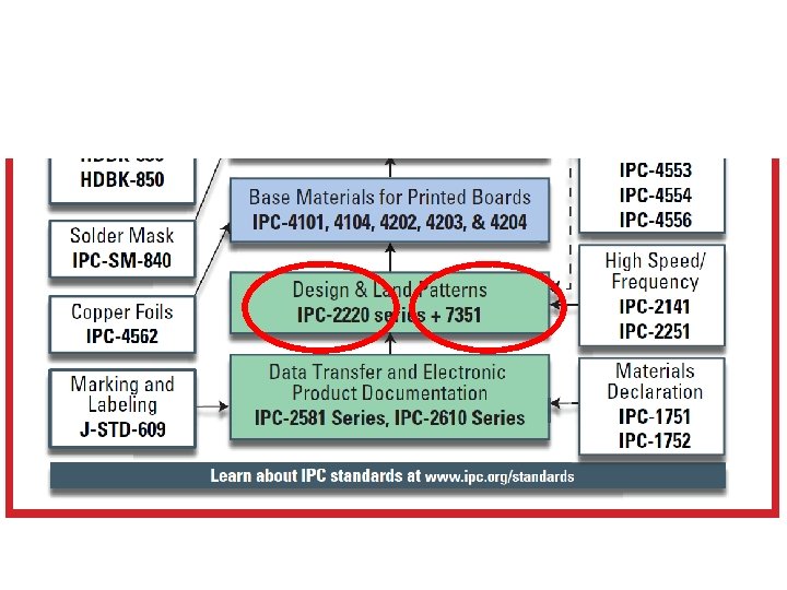
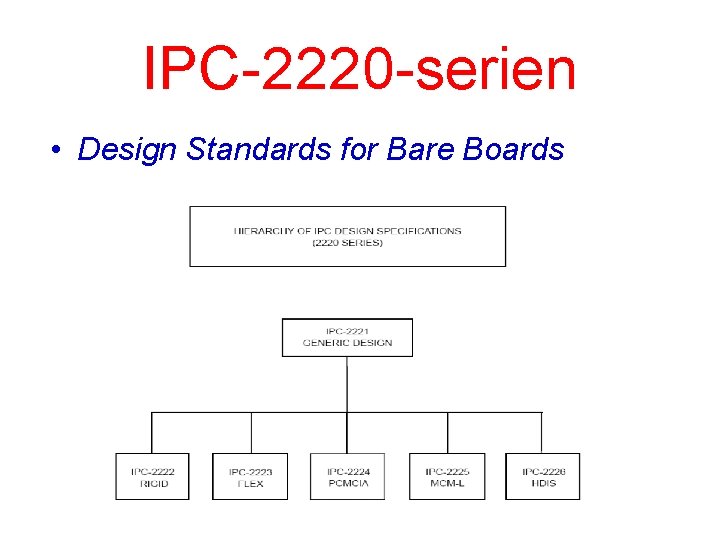
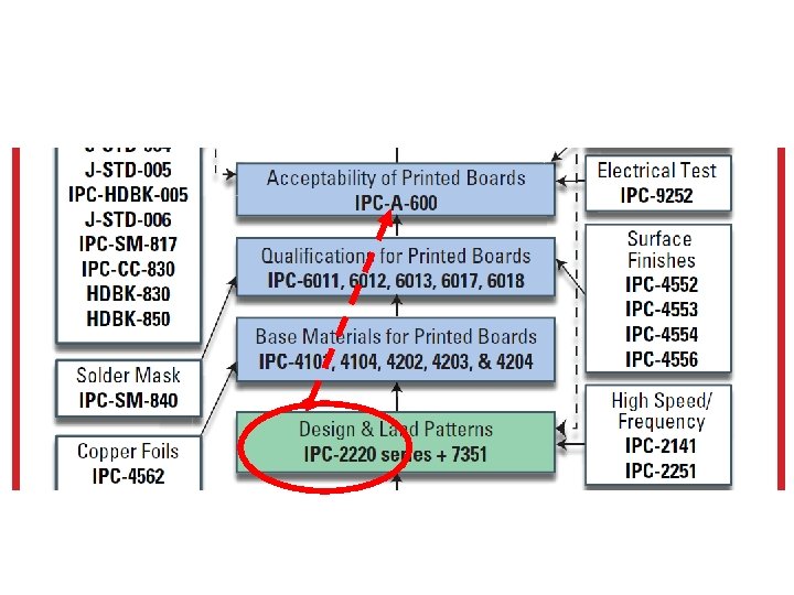
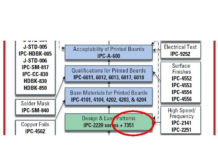
IPC-2220 -serien • Design Standards for Bare Boards

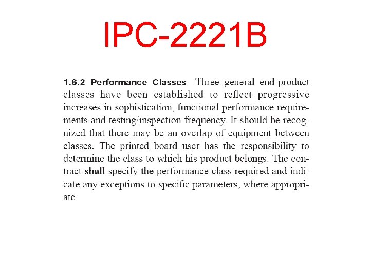
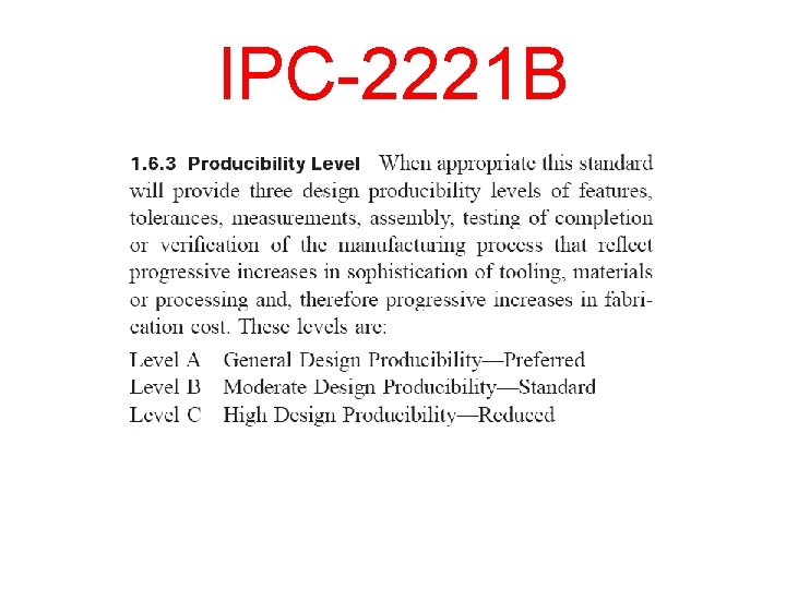
IPC-2221 B

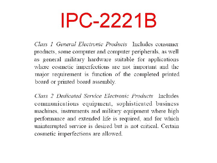
IPC-2221 B

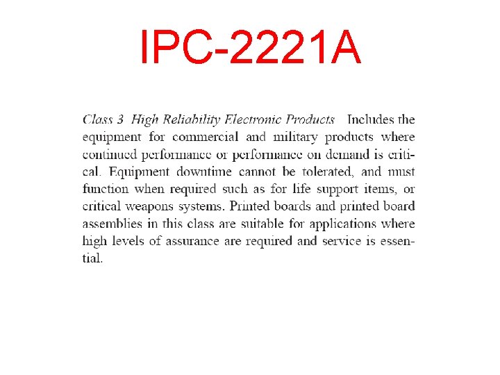
IPC-2221 A

IPC-2221 B

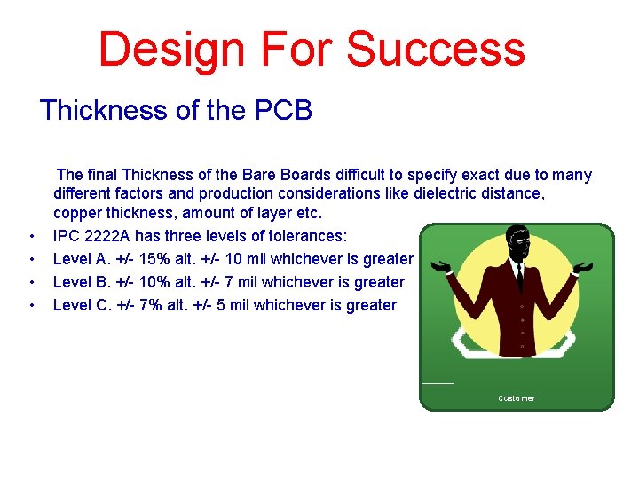
Design For Success Thickness of the PCB • • The final Thickness of the Bare Boards difficult to specify exact due to many different factors and production considerations like dielectric distance, copper thickness, amount of layer etc. IPC 2222 A has three levels of tolerances: Level A. +/- 15% alt. +/- 10 mil whichever is greater Level B. +/- 10% alt. +/- 7 mil whichever is greater Level C. +/- 7% alt. +/- 5 mil whichever is greater Customer

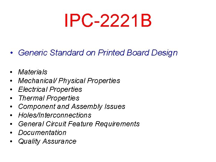
IPC-2221 B • Generic Standard on Printed Board Design • • • Materials Mechanical/ Physical Properties Electrical Properties Thermal Properties Component and Assembly Issues Holes/Interconnections General Circuit Feature Requirements Documentation Quality Assurance

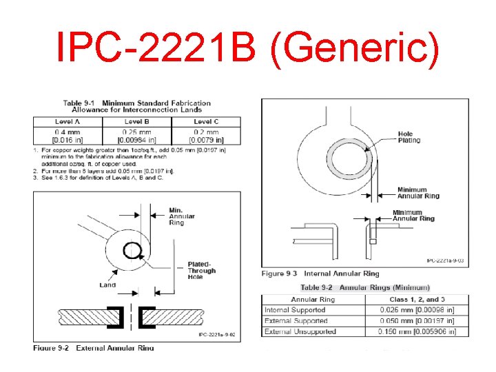
IPC-2221 B (Generic)

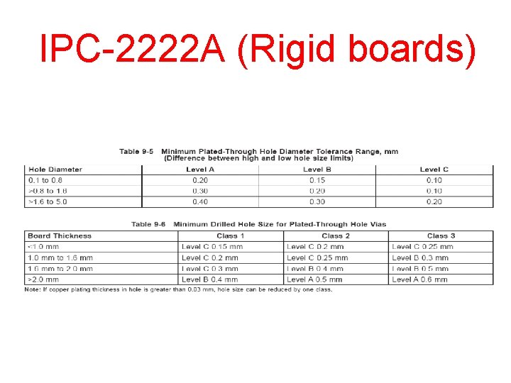
IPC-2222 A (Rigid boards)

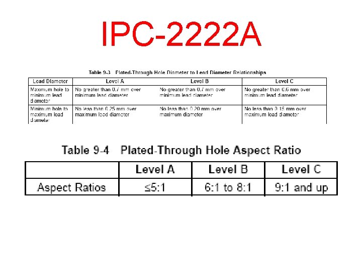
IPC-2222 A

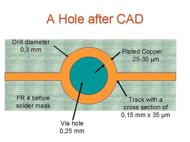
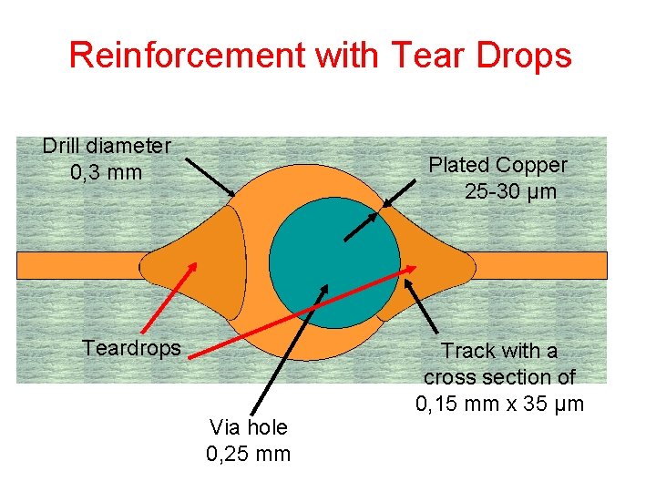
A Hole after CAD Drill diameter 0, 3 mm Plated Copper 25 -30 µm FR 4 before solder mask Track with a cross section of 0, 15 mm x 35 µm Via hole 0, 25 mm

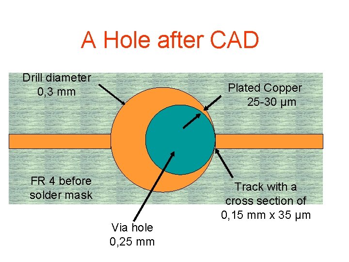
A Hole after CAD Drill diameter 0, 3 mm Plated Copper 25 -30 µm FR 4 before solder mask Via hole 0, 25 mm Track with a cross section of 0, 15 mm x 35 µm

Reinforcement with Tear Drops Drill diameter 0, 3 mm Plated Copper 25 -30 µm Teardrops Via hole 0, 25 mm Track with a cross section of 0, 15 mm x 35 µm

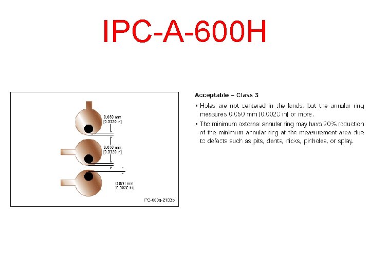
IPC-A-600 H

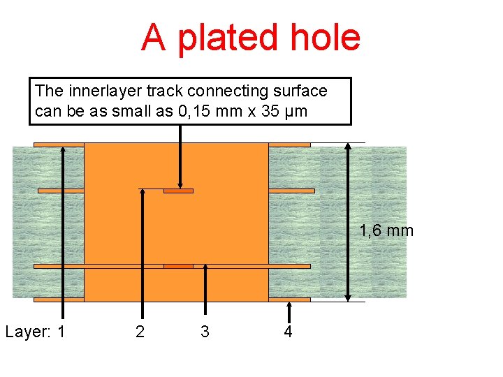
A plated hole The innerlayer track connecting surface can be as small as 0, 15 mm x 35 µm 1, 6 mm Layer: 1 2 3 4


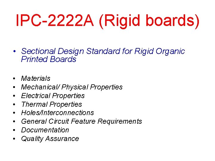
IPC-2222 A (Rigid boards) • Sectional Design Standard for Rigid Organic Printed Boards • • Materials Mechanical/ Physical Properties Electrical Properties Thermal Properties Holes/Interconnections General Circuit Feature Requirements Documentation Quality Assurance

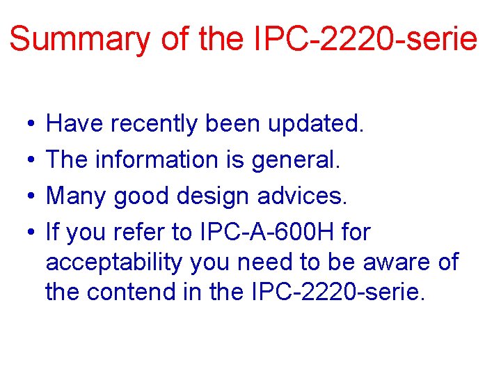
Summary of the IPC-2220 -serie • • Have recently been updated. The information is general. Many good design advices. If you refer to IPC-A-600 H for acceptability you need to be aware of the contend in the IPC-2220 -serie.


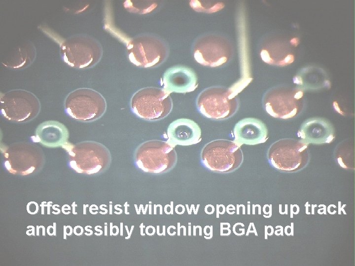
Offset resist window opening up track and possibly touching BGA pad

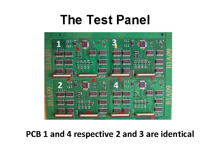
The Test Panel 1 3 2 4 PCB 1 and 4 respective 2 and 3 are identical

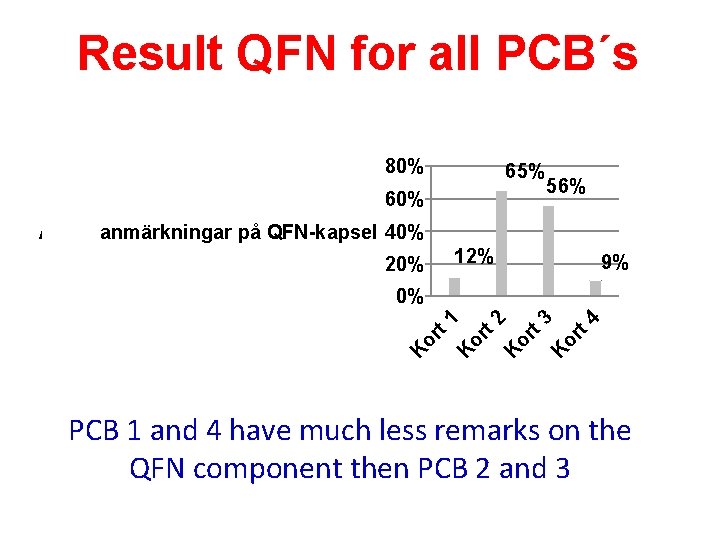
Result QFN for all PCB´s 80% 65% 60% 56% Andel anmärkningar på QFN-kapsel 40% 12% 20% 9% t 4 or K t 3 or K t 2 or K K or t 1 0% PCB 1 and 4 have much less remarks on the QFN component then PCB 2 and 3

IPC Standards which include Lead Free • For CAD: • IPC-7351 B. • Supersedes – IPC-7351 A, IPC-7351 and IPC-SM-782.

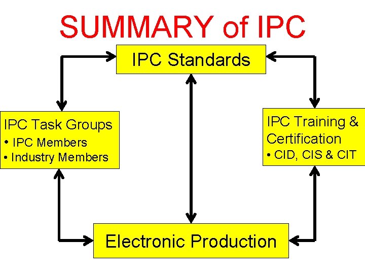
SUMMARY of IPC Standards IPC Task Groups • IPC Members • Industry Members IPC Training & Certification • CID, CIS & CIT Electronic Production

Produkt spec Component data Electonic scheme Net List BOM IPC-2141 A IPC-2251 IPC-2152 IPC-7093 IPC-7094 J-STD-609 A IPC-1752 A IPC-2610 • Designer Certification: • IPC PCB Basic Designer (CID) • IPC PCB Advanced Designer (CID+) IPC-2221 B IPC-2222 A IPC-7351 B IPC-7525 B IPC-7527 IPC-7095 C

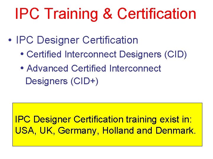
IPC Training & Certification • IPC Designer Certification • Certified Interconnect Designers (CID) • Advanced Certified Interconnect Designers (CID+) IPC Designer Certification training exist in: USA, UK, Germany, Holland Denmark.

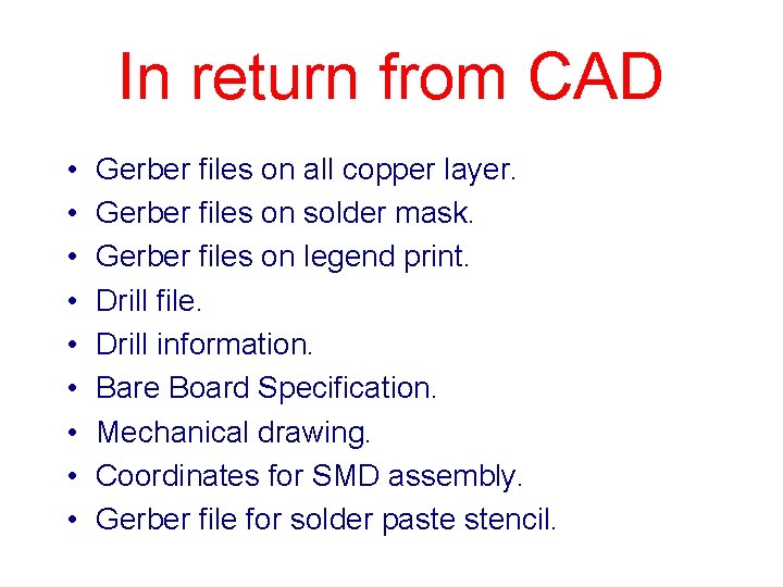
In return from CAD • • • Gerber files on all copper layer. Gerber files on solder mask. Gerber files on legend print. Drill file. Drill information. Bare Board Specification. Mechanical drawing. Coordinates for SMD assembly. Gerber file for solder paste stencil.

Product spec Please Fill In!! Component data Electronic scheme Routing Net list BOM IPC-2141 A IPC-2251 IPC-2152 IPC-7093 IPC-7094 J-STD-609 A IPC-1752 A IPC-2610 Gerber files Drill files Bare Board Spec Footprints Component placement IPC-2221 B IPC-2222 A IPC-7351 B IPC-2581 IPC-7095 C IPC-7527 Program for: -Laser Plotter -Drilling -Routing -AOI -Electric test To Bare Board Production


Practical Advice You need an IPC Checklist!!
