IPC Compliance Testing DPA Methodology Oct 3 2019

- Slides: 33

IPC Compliance Testing (DPA) Methodology Oct. 3, 2019 Prepared by Roger Jay roger@covalentmetrology. com

DPA: Introduction 2 • Destructive Physical Analysis (DPA) is a comprehensive quality assessment for workmanship on Printed Circuit Board Assemblies (PCBAs). • The Best-Known Method for determining quality of boards, components, design, and assembly processes. Sample size is typically one assembly. • Performed using non-destructive and destructive inspections: external visual, X-ray, and cross-sectioning. • Workmanship conditions are determined as Target, Acceptable, Process Indicator, or Defect based on IPC-A-610 G for the applicable product class (Class II typical for data center products).

DPA: Introduction 3 • Plated Through Hole (PTH) locations are typically included to determine internal board fabrication conditions as Target, Acceptable, or Non. Conforming based on IPC-A-600 H. • Ionic Cleanliness testing can be added to determine if assembly process residues are benign. This includes Critical Cleanliness Control (C 3) spot testing for local areas and Full Bag Extraction for cleanliness of the entire assembly. • Rinse fluid from these tests can be analyzed with Ion Chromatography (IC) to identify and quantify the ionic species extracted. These test are used for compliance with IPC-A-610 G.

DPA: Techniques – External Visual & X-ray Inspection 4 • External visual inspection utilizes a stereo-zoom microscope and a small hand -held mirror to inspect solder fillets, pin alignment, BGA solder balls (outer rows), contamination, reference designator markings, etc. • X-ray allows non-destructive internal inspection for voids, pin alignment, press -fit connections, solder fill, PTH plating issues, etc. • Any locations showing questionable workmanship from external visual or Xray, such as hole-fill, fillet height, solder cracks, etc. should be verified by cross-sectioning.

DPA: Techniques – Cross-sectioning 5 • Cross-sectioning is a destructive technique that physically slices into the features of a component or board that are targeted for inspection. • The extracted components are encapsulated in epoxy to protect the features while they are ground and polished to show details of their internal structure. • This method is often used to confirm workmanship for fillet height, hole-fill, press -fit pins, solder cracks, wetting issues, solder balls, PTH plating quality, delamination, etc. • Representative devices typically includes Connectors, BGAs, Capacitors, PLCCs and any device showing questionable workmanship from the other inspections.

6

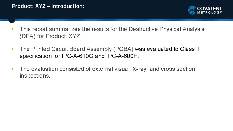
Product: XYZ – Introduction: 7 • This report summarizes the results for the Destructive Physical Analysis (DPA) for Product: XYZ. • The Printed Circuit Board Assembly (PCBA) was evaluated to Class II specification for IPC-A-610 G and IPC-A-600 H. • The evaluation consisted of external visual, X-ray, and cross section inspections.

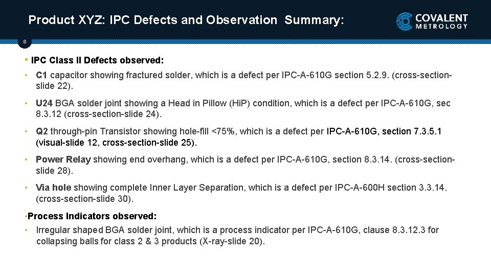
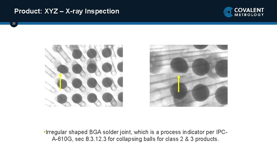
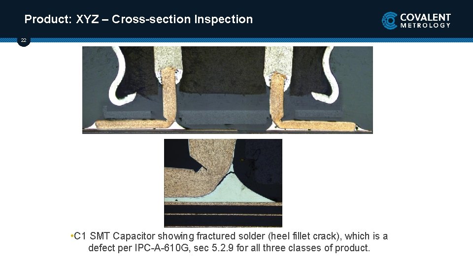
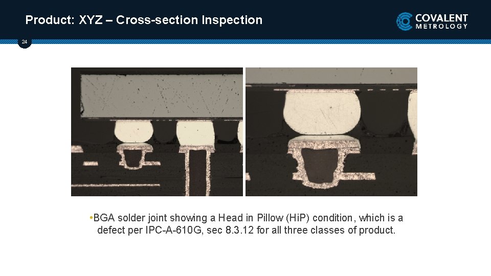
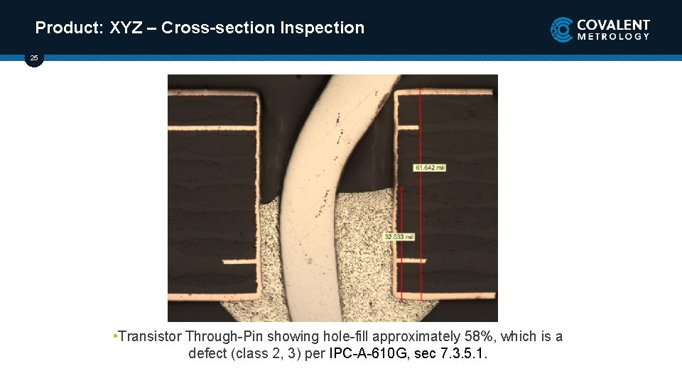
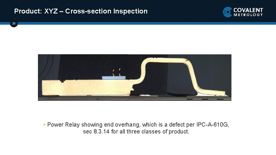
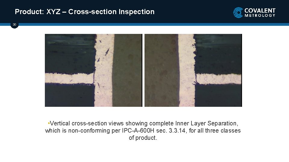
Product XYZ: IPC Defects and Observation Summary: 8 • IPC Class II Defects observed: • C 1 capacitor showing fractured solder, which is a defect per IPC-A-610 G section 5. 2. 9. (cross-sectionslide 22). • U 24 BGA solder joint showing a Head in Pillow (Hi. P) condition, which is a defect per IPC-A-610 G, sec 8. 3. 12 (cross-section-slide 24). • Q 2 through-pin Transistor showing hole-fill <75%, which is a defect per IPC-A-610 G, section 7. 3. 5. 1 (visual-slide 12, cross-section-slide 25). • Power Relay showing end overhang, which is a defect per IPC-A-610 G, section 8. 3. 14. (cross-sectionslide 28). • Via hole showing complete Inner Layer Separation, which is a defect per IPC-A-600 H section 3. 3. 14. (cross-section-slide 30). • Process Indicators observed: • Irregular shaped BGA solder joint, which is a process indicator per IPC-A-610 G, clause 8. 3. 12. 3 for collapsing balls for class 2 & 3 products (X-ray-slide 20).

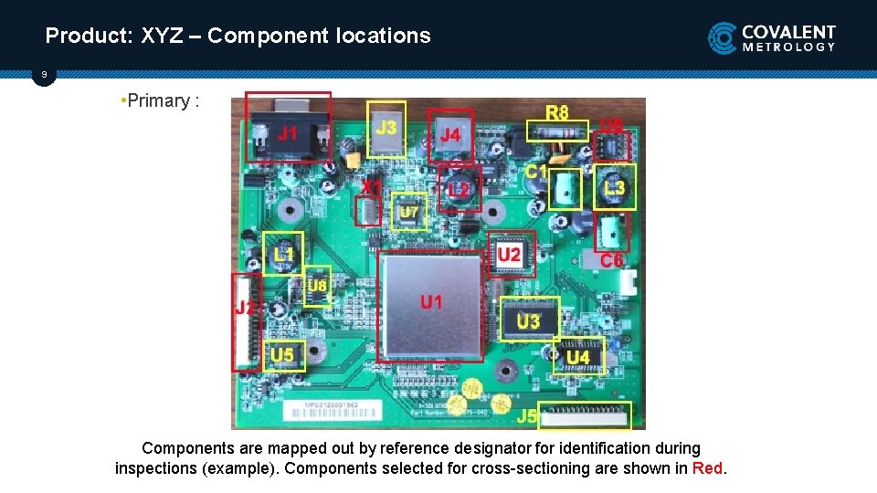
Product: XYZ – Component locations 9 • Primary : Components are mapped out by reference designator for identification during inspections (example). Components selected for cross-sectioning are shown in Red.

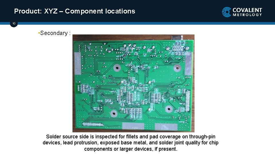
Product: XYZ – Component locations 10 • Secondary : Solder source side is inspected for fillets and pad coverage on through-pin devices, lead protrusion, exposed base metal, and solder joint quality for chip components or larger devices, if present.

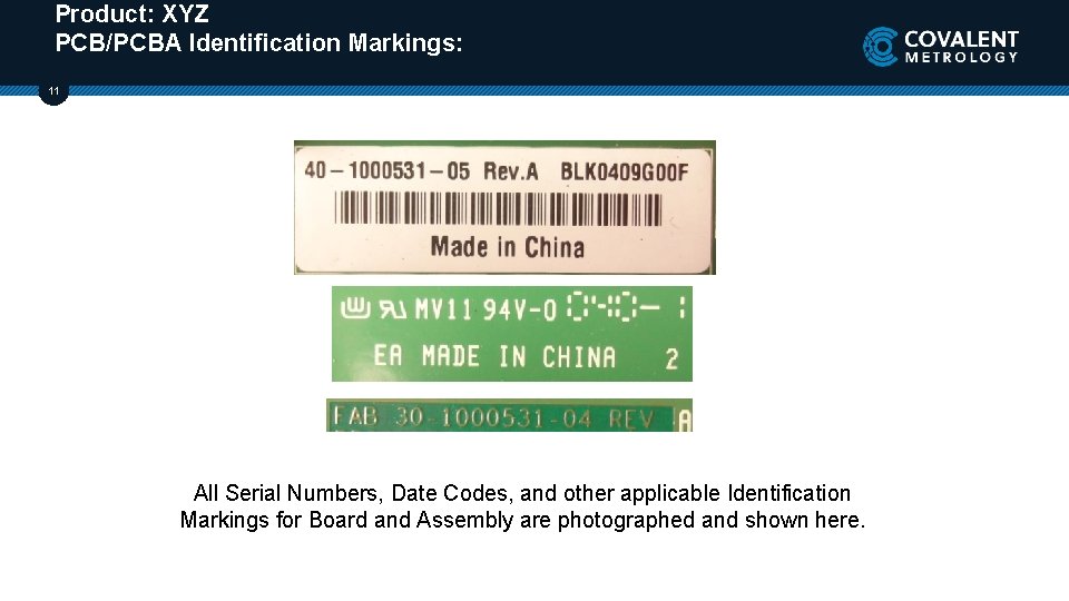
Product: XYZ PCB/PCBA Identification Markings: 11 All Serial Numbers, Date Codes, and other applicable Identification Markings for Board and Assembly are photographed and shown here.

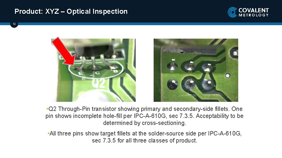
Product: XYZ – Optical Inspection 12 • Q 2 Through-Pin transistor showing primary and secondary-side fillets. One pin shows incomplete hole-fill per IPC-A-610 G, sec 7. 3. 5. Acceptability to be determined by cross-sectioning. • All three pins show target fillets at the solder-source side per IPC-A-610 G, sec 7. 3. 5 for all three classes of product.

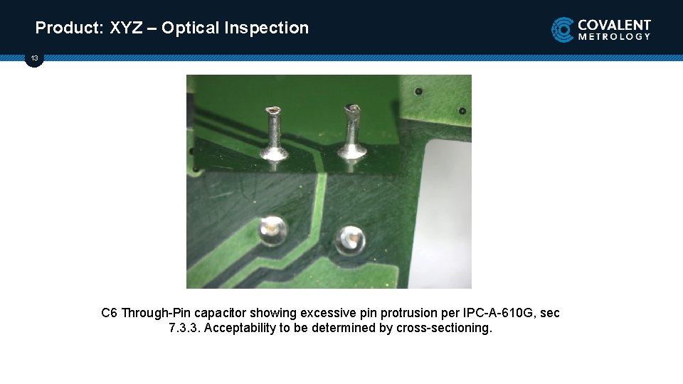
Product: XYZ – Optical Inspection 13 C 6 Through-Pin capacitor showing excessive pin protrusion per IPC-A-610 G, sec 7. 3. 3. Acceptability to be determined by cross-sectioning.

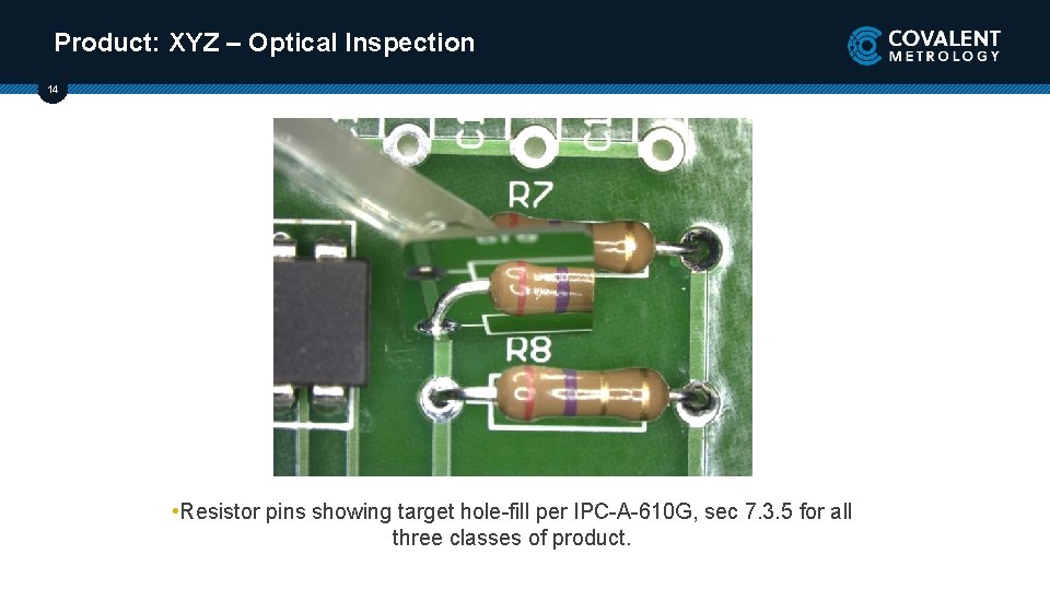
Product: XYZ – Optical Inspection 14 • Resistor pins showing target hole-fill per IPC-A-610 G, sec 7. 3. 5 for all three classes of product.

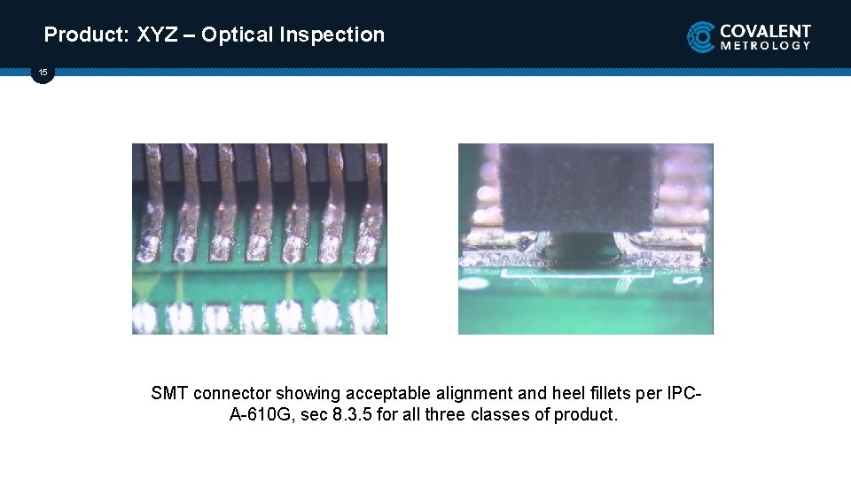
Product: XYZ – Optical Inspection 15 SMT connector showing acceptable alignment and heel fillets per IPCA-610 G, sec 8. 3. 5 for all three classes of product.

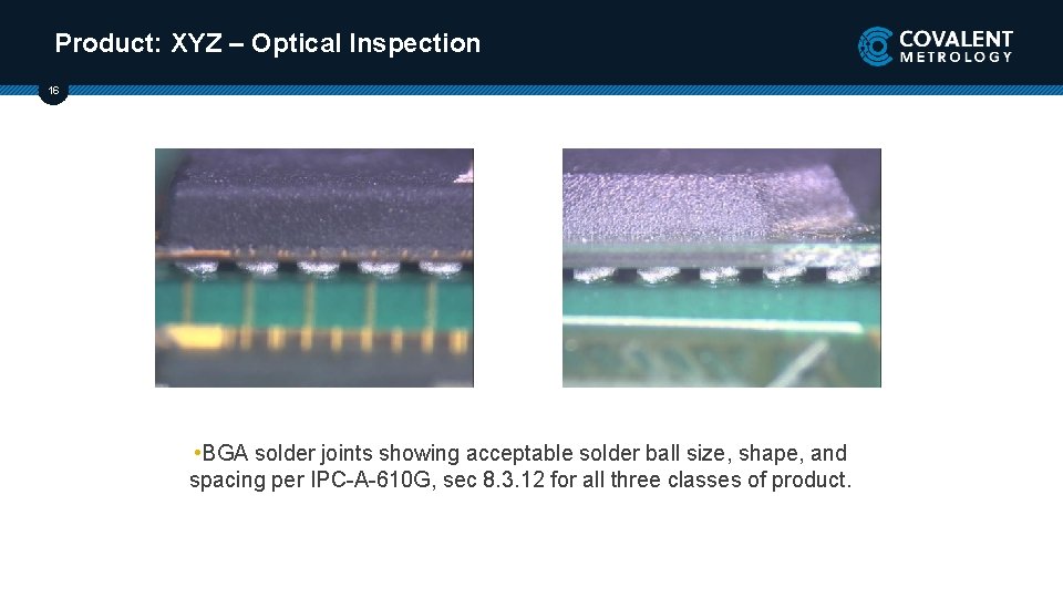
Product: XYZ – Optical Inspection 16 • BGA solder joints showing acceptable solder ball size, shape, and spacing per IPC-A-610 G, sec 8. 3. 12 for all three classes of product.

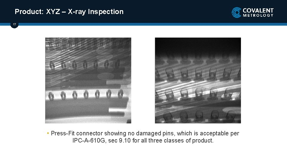
Product: XYZ – X-ray Inspection 17 • Press-Fit connector showing no damaged pins, which is acceptable per IPC-A-610 G, sec 9. 10 for all three classes of product.

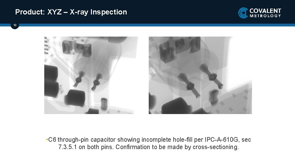
Product: XYZ – X-ray Inspection 18 • C 6 through-pin capacitor showing incomplete hole-fill per IPC-A-610 G, sec 7. 3. 5. 1 on both pins. Confirmation to be made by cross-sectioning.

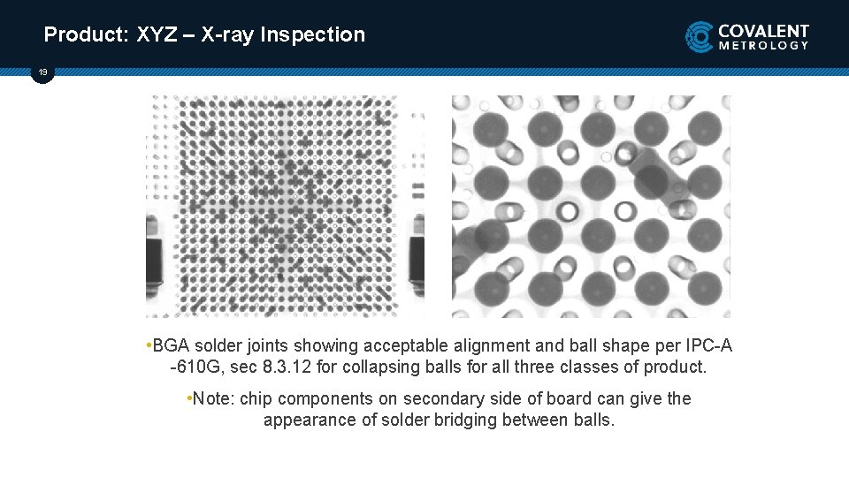
Product: XYZ – X-ray Inspection 19 • BGA solder joints showing acceptable alignment and ball shape per IPC-A -610 G, sec 8. 3. 12 for collapsing balls for all three classes of product. • Note: chip components on secondary side of board can give the appearance of solder bridging between balls.

Product: XYZ – X-ray Inspection 20 • Irregular shaped BGA solder joint, which is a process indicator per IPCA-610 G, sec 8. 3. 12. 3 for collapsing balls for class 2 & 3 products.

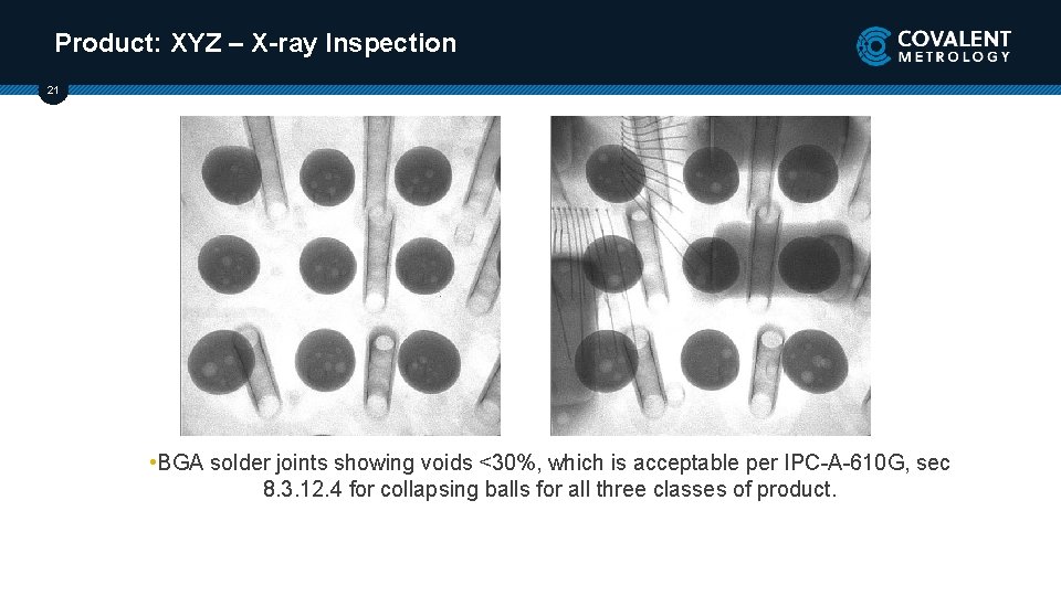
Product: XYZ – X-ray Inspection 21 • BGA solder joints showing voids <30%, which is acceptable per IPC-A-610 G, sec 8. 3. 12. 4 for collapsing balls for all three classes of product.

Product: XYZ – Cross-section Inspection 22 • C 1 SMT Capacitor showing fractured solder (heel fillet crack), which is a defect per IPC-A-610 G, sec 5. 2. 9 for all three classes of product.

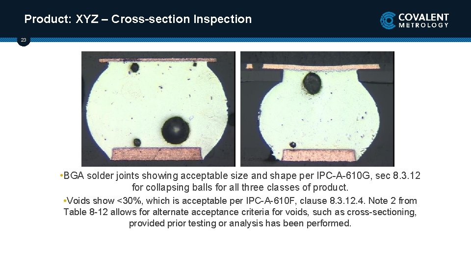
Product: XYZ – Cross-section Inspection 23 • BGA solder joints showing acceptable size and shape per IPC-A-610 G, sec 8. 3. 12 for collapsing balls for all three classes of product. • Voids show <30%, which is acceptable per IPC-A-610 F, clause 8. 3. 12. 4. Note 2 from Table 8 -12 allows for alternate acceptance criteria for voids, such as cross-sectioning, provided prior testing or analysis has been performed.

Product: XYZ – Cross-section Inspection 24 • BGA solder joint showing a Head in Pillow (Hi. P) condition, which is a defect per IPC-A-610 G, sec 8. 3. 12 for all three classes of product.

Product: XYZ – Cross-section Inspection 25 • Transistor Through-Pin showing hole-fill approximately 58%, which is a defect (class 2, 3) per IPC-A-610 G, sec 7. 3. 5. 1.

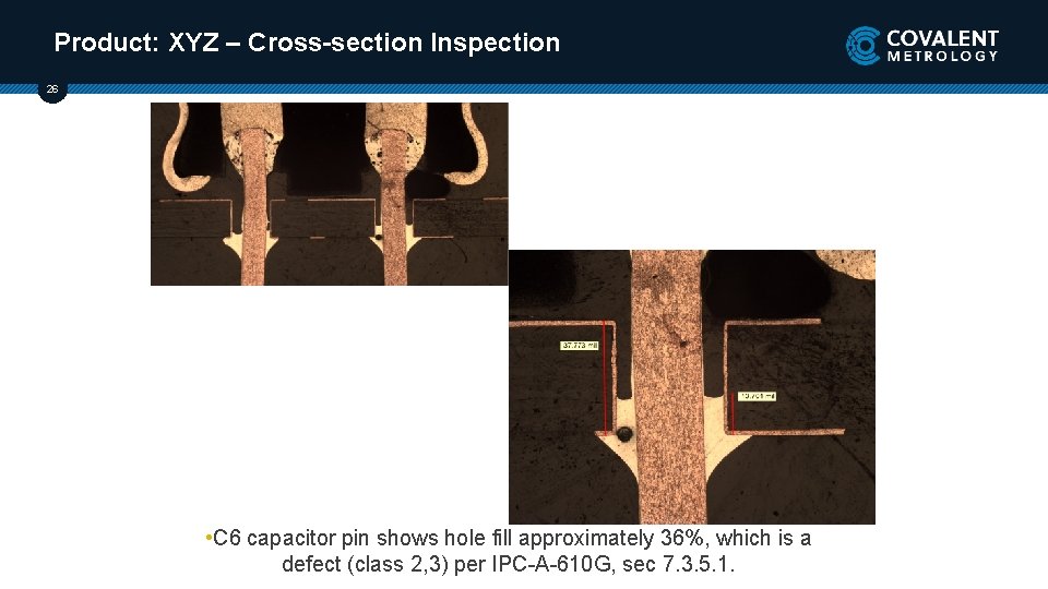
Product: XYZ – Cross-section Inspection 26 • C 6 capacitor pin shows hole fill approximately 36%, which is a defect (class 2, 3) per IPC-A-610 G, sec 7. 3. 5. 1.

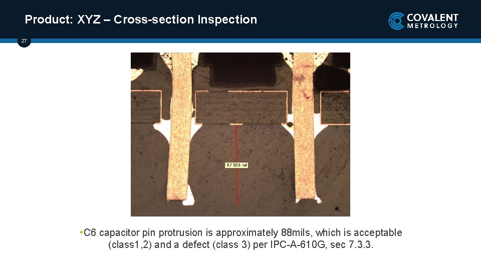
Product: XYZ – Cross-section Inspection 27 • C 6 capacitor pin protrusion is approximately 88 mils, which is acceptable (class 1, 2) and a defect (class 3) per IPC-A-610 G, sec 7. 3. 3.

Product: XYZ – Cross-section Inspection 28 • Power Relay showing end overhang, which is a defect per IPC-A-610 G, sec 8. 3. 14 for all three classes of product.

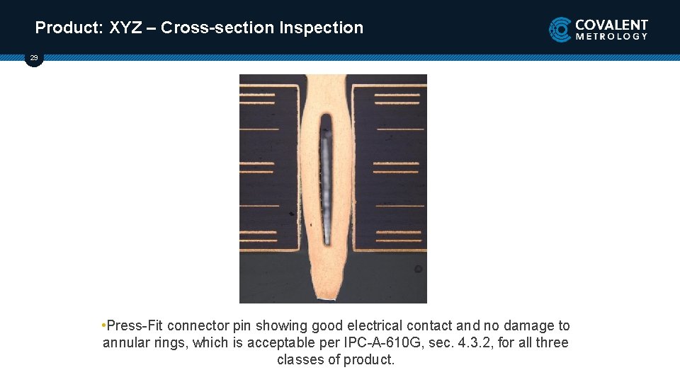
Product: XYZ – Cross-section Inspection 29 • Press-Fit connector pin showing good electrical contact and no damage to annular rings, which is acceptable per IPC-A-610 G, sec. 4. 3. 2, for all three classes of product.

Product: XYZ – Cross-section Inspection 30 • Vertical cross-section views showing complete Inner Layer Separation, which is non-conforming per IPC-A-600 H sec. 3. 3. 14, for all three classes of product.

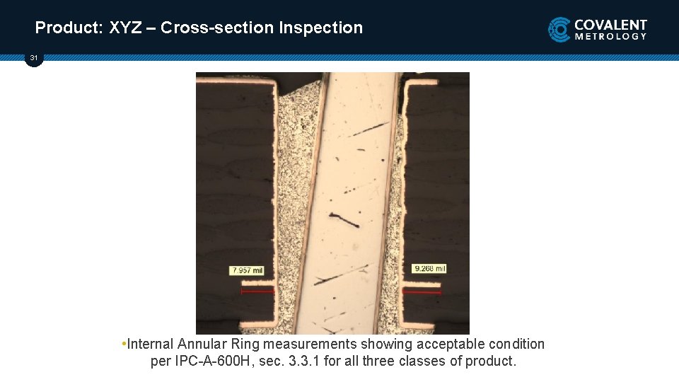
Product: XYZ – Cross-section Inspection 31 • Internal Annular Ring measurements showing acceptable condition per IPC-A-600 H, sec. 3. 3. 1 for all three classes of product.

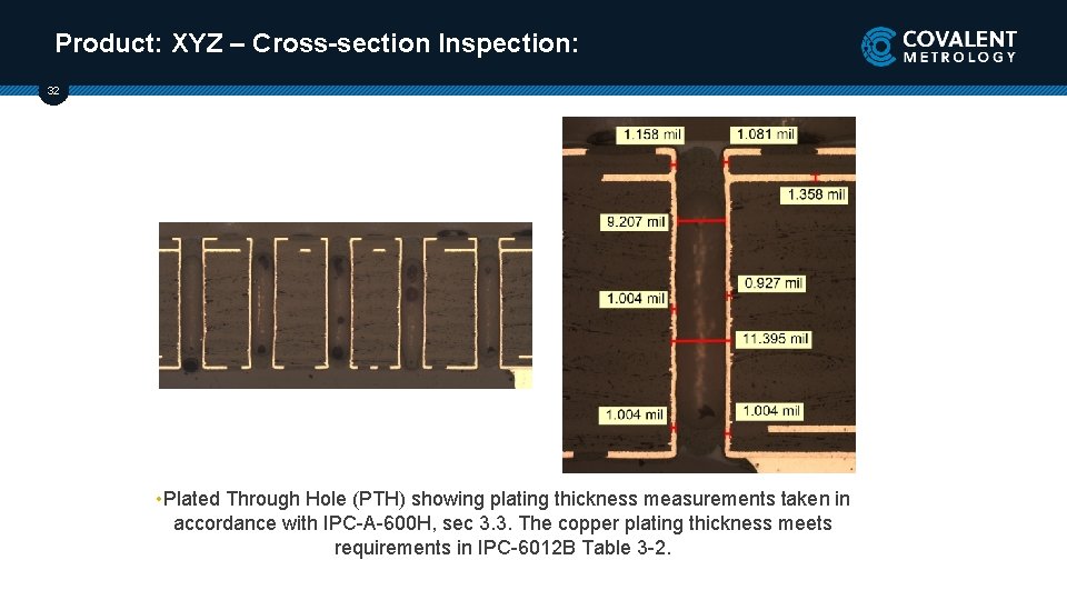
Product: XYZ – Cross-section Inspection: 32 • Plated Through Hole (PTH) showing plating thickness measurements taken in accordance with IPC-A-600 H, sec 3. 3. The copper plating thickness meets requirements in IPC-6012 B Table 3 -2.

Thank You covalentmetrology. com