ION ENERGY AND ANGULAR DISTRIBUTIONS INTO SMALL FEATURES
ION ENERGY AND ANGULAR DISTRIBUTIONS INTO SMALL FEATURES IN PLASMA ETCHING REACTORS: THE WAFER- FOCUS RING GAP* Natalia Yu. Babaeva and Mark J. Kushner Iowa State University Department of Electrical and Computer Engineering Ames, IA 50011, USA natalie 5@iastate. edu mjk@iastate. edu http: //uigelz. ece. iastate. edu AVS 54 th International Symposium October 2007 * Work supported by Semiconductor Research Corp. , Applied Materials and NSF AVS 2007_Natalie_01
AGENDA · Wafer edge effects · Description of the model · Ion energy and angular distribution on different surfaces in wafer-focus ring gap for focus ring: · Capacitance · Height · Conductivity · Concluding remarks AVS 2007_Natalie_02 Iowa State University Optical and Discharge Physics
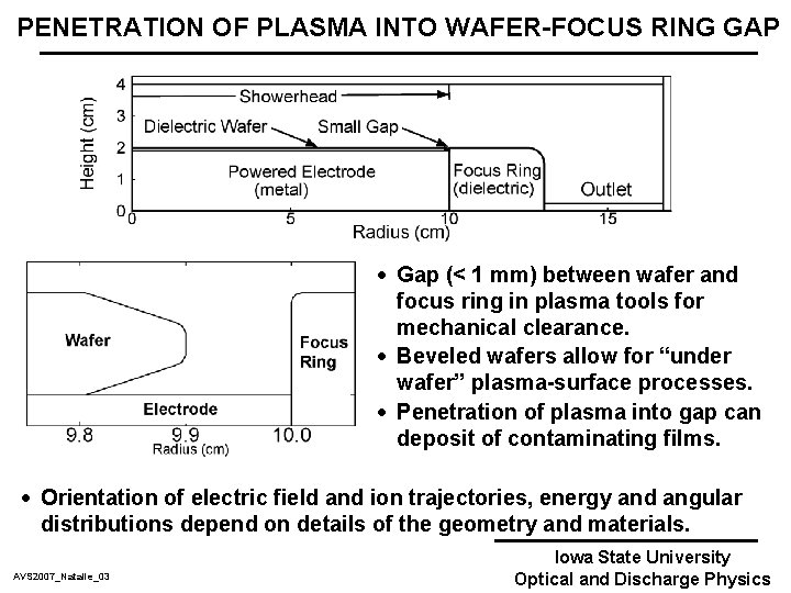
PENETRATION OF PLASMA INTO WAFER-FOCUS RING GAP · Gap (< 1 mm) between wafer and focus ring in plasma tools for mechanical clearance. · Beveled wafers allow for “under wafer” plasma-surface processes. · Penetration of plasma into gap can deposit of contaminating films. · Orientation of electric field and ion trajectories, energy and angular distributions depend on details of the geometry and materials. AVS 2007_Natalie_03 Iowa State University Optical and Discharge Physics
INVESTIGATION OF IEADs INTO WAFER-FOCUS RING GAP · The ion energy and angular distributions (IEADs) into the wafer-focus ring gap are important; · Angular distribution determines erosion (e. g. , maximum sputtering at 60 o. · Time between replacement of consumable parts depends on erosion. · Spacing, materials (e. g. , dielectric constant, conductivity) determine electric field in gap and so IEADS. · In this presentation, results from a computational investigation of IEADs onto surfaces in wafer-focus ring gap will be discussed. · Model: non. PDPSIM using unstructured meshes. · Goal: How does one control the IEADs? AVS 2007_Natalie_03 Iowa State University Optical and Discharge Physics
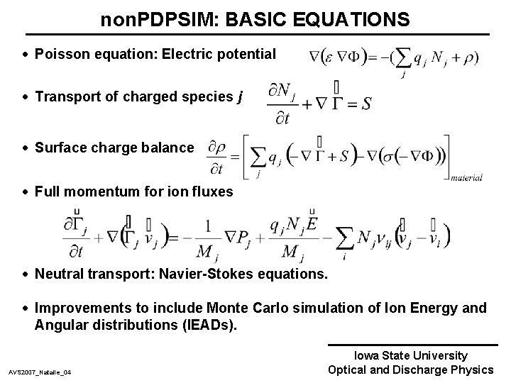
non. PDPSIM: BASIC EQUATIONS · Poisson equation: Electric potential · Transport of charged species j · Surface charge balance · Full momentum for ion fluxes · Neutral transport: Navier-Stokes equations. · Improvements to include Monte Carlo simulation of Ion Energy and Angular distributions (IEADs). AVS 2007_Natalie_04 Iowa State University Optical and Discharge Physics
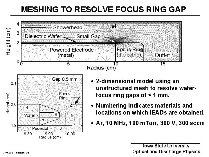
MESHING TO RESOLVE FOCUS RING GAP · 2 -dimensional model using an unstructured mesh to resolve waferfocus ring gaps of < 1 mm. · Numbering indicates materials and locations on which IEADs are obtained. · Ar, 10 MHz, 100 m. Torr, 300 V, 300 sccm AVS 2007_Natalie_05 Iowa State University Optical and Discharge Physics
![POTENTIAL, ELECTRIC FIELD, IONS Potential · Off-axis maximum in [Ar+] is due to electric POTENTIAL, ELECTRIC FIELD, IONS Potential · Off-axis maximum in [Ar+] is due to electric](http://slidetodoc.com/presentation_image_h/1ac6e9a7278ed0f8dffc524205d482f7/image-7.jpg)
POTENTIAL, ELECTRIC FIELD, IONS Potential · Off-axis maximum in [Ar+] is due to electric field enhancement near focus ring and is uncorrelated to gap. E/N · Ar, 10 MHz, 100 m. Torr, 300 V [Ar+] AVS 2007_Natalie_06 MIN MAX · Gap: 1 mm Iowa State University Optical and Discharge Physics
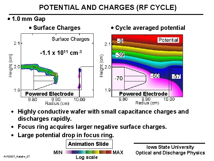
POTENTIAL AND CHARGES (RF CYCLE) 1. 0 mm Gap Surface Charges Cycle averaged potential -1. 1 x 1011 cm-3 Powered Electrode · Highly conductive wafer with small capacitance charges and discharges rapidly. · Focus ring acquires larger negative surface charges. · Large potential drop in focus ring. Animation Slide AVS 2007_Natalie_07 MIN Log scale MAX Iowa State University Optical and Discharge Physics
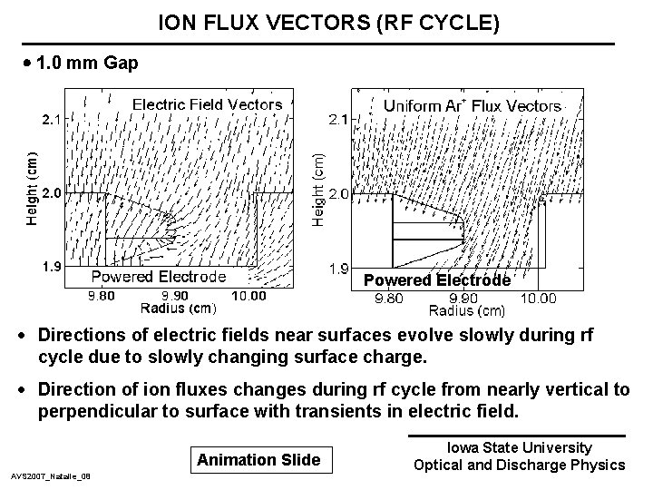
ION FLUX VECTORS (RF CYCLE) 1. 0 mm Gap Powered Electrode · Directions of electric fields near surfaces evolve slowly during rf cycle due to slowly changing surface charge. · Direction of ion fluxes changes during rf cycle from nearly vertical to perpendicular to surface with transients in electric field. Animation Slide AVS 2007_Natalie_08 Iowa State University Optical and Discharge Physics
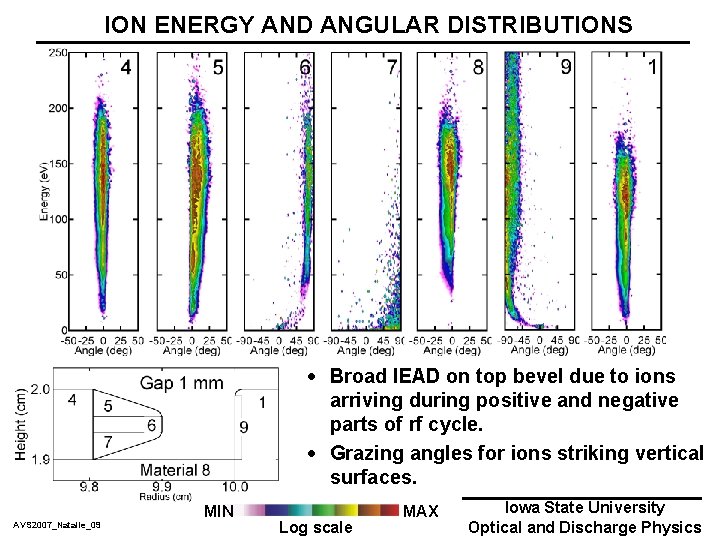
ION ENERGY AND ANGULAR DISTRIBUTIONS · Broad IEAD on top bevel due to ions arriving during positive and negative parts of rf cycle. · Grazing angles for ions striking vertical surfaces. AVS 2007_Natalie_09 MIN Log scale MAX Iowa State University Optical and Discharge Physics
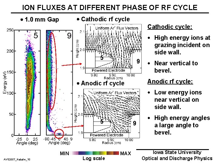
ION FLUXES AT DIFFERENT PHASE OF RF CYCLE Cathodic rf cycle 1. 0 mm Gap Cathodic cycle: · High energy ions at grazing incident on side wall. 5 9 · Near vertical to bevel. Anodic rf cycle: Anodic rf cycle · Low energy ions near vertical on side wall. 5 MIN AVS 2007_Natalie_10 Log scale 9 MAX · High energy angles a large angle to bevel. Iowa State University Optical and Discharge Physics
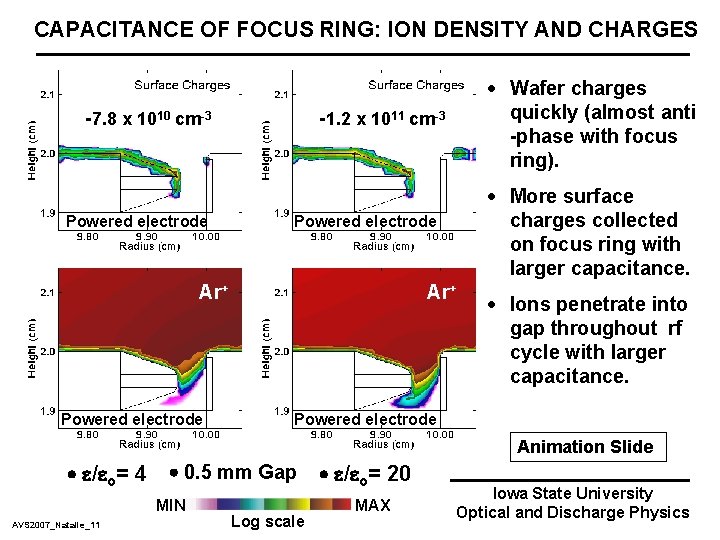
CAPACITANCE OF FOCUS RING: ION DENSITY AND CHARGES · Wafer charges quickly (almost anti -phase with focus ring). 1. 0 mm Gap -7. 8 x 1010 cm-3 -1. 2 x 1011 cm-3 Powered electrode Ar+ Powered electrode · More surface charges collected on focus ring with larger capacitance. Ar+ · Ions penetrate into gap throughout rf cycle with larger capacitance. Powered electrode Animation Slide / o= 4 0. 5 mm Gap MIN AVS 2007_Natalie_11 Log scale / o= 20 MAX Iowa State University Optical and Discharge Physics
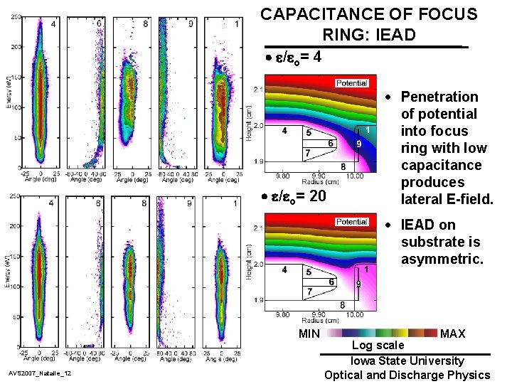
CAPACITANCE OF FOCUS RING: IEAD / o= 4 / o= 20 · Penetration of potential into focus ring with low capacitance produces lateral E-field. · IEAD on substrate is asymmetric. MIN AVS 2007_Natalie_12 MAX Log scale Iowa State University Optical and Discharge Physics
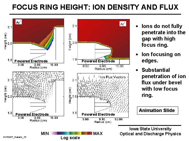
FOCUS RING HEIGHT: ION DENSITY AND FLUX 1. 0 mm Gap Powered Electrode · Ions do not fully penetrate into the gap with high focus ring. Powered Electrode · Ion focusing on edges. · Substantial penetration of ion flux under bevel with low focus ring. Powered Electrode AVS 2007_Natalie_13 MIN Powered Electrode Log scale MAX Animation Slide Iowa State University Optical and Discharge Physics
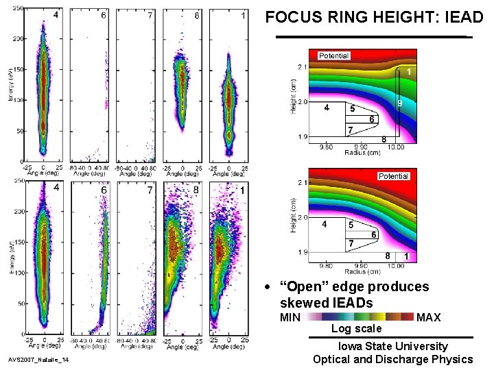
FOCUS RING HEIGHT: IEAD 1. 0 mm Gap 0. 25 mm Gap · “Open” edge produces skewed IEADs MIN AVS 2007_Natalie_14 Log scale MAX Iowa State University Optical and Discharge Physics
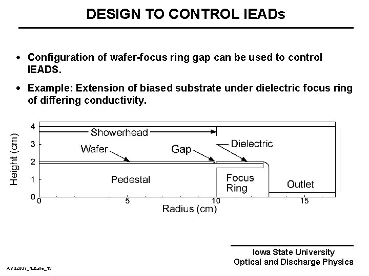
DESIGN TO CONTROL IEADs · Configuration of wafer-focus ring gap can be used to control IEADS. · Example: Extension of biased substrate under dielectric focus ring of differing conductivity. AVS 2007_Natalie_15 Iowa State University Optical and Discharge Physics
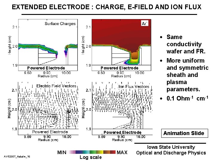
EXTENDED ELECTRODE : CHARGE, E-FIELD AND ION FLUX · Same conductivity wafer and FR. Powered Electrode · More uniform and symmetric sheath and plasma parameters. · 0. 1 Ohm-1 cm-1 Powered Electrode AVS 2007_Natalie_16 MIN Log scale MAX Animation Slide Iowa State University Optical and Discharge Physics
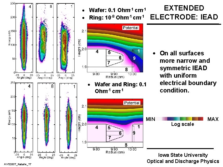
· Wafer: 0. 1 Ohm-1 cm-1 · Ring: 10 -8 Ohm-1 cm-1 EXTENDED ELECTRODE: IEAD · On all surfaces more narrow and symmetric IEAD with uniform electrical boundary · Wafer and Ring: 0. 1 condition. Ohm-1 cm-1 MIN AVS 2007_Natalie_17 Log scale MAX Iowa State University Optical and Discharge Physics
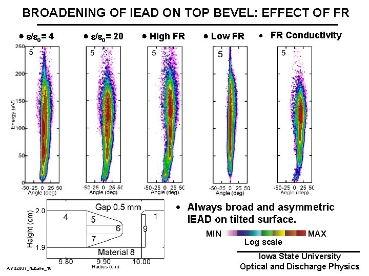
BROADENING OF IEAD ON TOP BEVEL: EFFECT OF FR / o= 4 / o= 20 High FR Low FR · FR Conductivity · Always broad and asymmetric IEAD on tilted surface. MIN AVS 2007_Natalie_18 Log scale MAX Iowa State University Optical and Discharge Physics
CONCLUDING REMARKS · Ion energy and angular distributions were investigated on surfaces inside wafer-focus ring gap. · Different regions of the IEADs are generated during different parts of the rf cycle. Even vertical surfaces receive some normal angle ion flux. · Narrow IEAD are obtained with · High focus ring capacitance · High focus ring conductivity. · Uniform electrical boundary conditions leads to more symmetric sheath over the gap and narrows IEADs. · On tilted surfaces broad and asymmetric IEADs are obtained for most conditions. AVS 2006_Natalie_19 Iowa State University Optical and Discharge Physics
- Slides: 20