IO Port Programming Port 1pins 1 8 Port
- Slides: 30

I/O Port Programming Port 1(pins 1 -8) • Port 1 is denoted by P 1. – P 1. 0 ~ P 1. 7 • We use P 1 as examples to show the operations on ports. – P 1 as an output port (i. e. , write CPU data to the external pin) – P 1 as an input port (i. e. , read pin data into CPU bus) 4/10/2007 ESD, USIT, GGSIPU 1

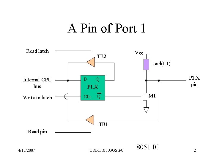
A Pin of Port 1 Read latch TB 2 Vcc Load(L 1) Internal CPU bus D Write to latch Clk P 1. X pin Q P 1. X Q M 1 TB 1 Read pin 4/10/2007 ESD, USIT, GGSIPU 8051 IC 2

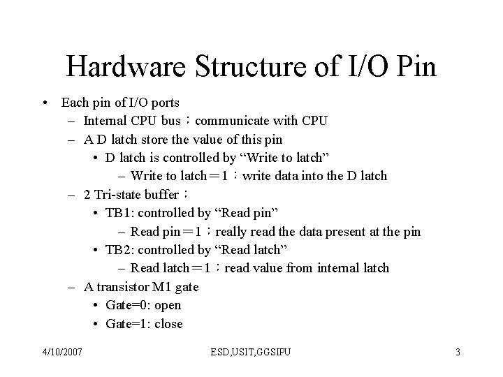
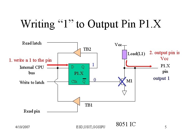
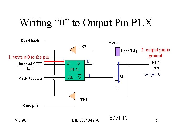
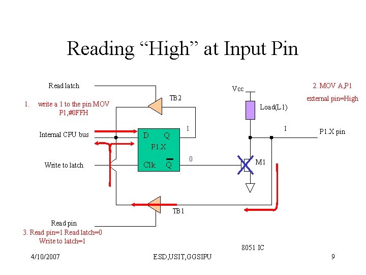
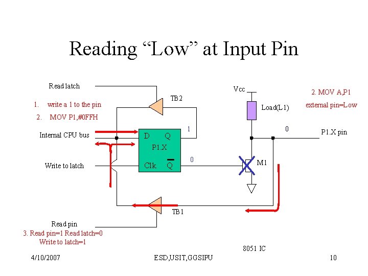
Hardware Structure of I/O Pin • Each pin of I/O ports – Internal CPU bus:communicate with CPU – A D latch store the value of this pin • D latch is controlled by “Write to latch” – Write to latch= 1:write data into the D latch – 2 Tri-state buffer: • TB 1: controlled by “Read pin” – Read pin= 1:really read the data present at the pin • TB 2: controlled by “Read latch” – Read latch= 1:read value from internal latch – A transistor M 1 gate • Gate=0: open • Gate=1: close 4/10/2007 ESD, USIT, GGSIPU 3

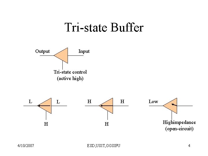
Tri-state Buffer Output Input Tri-state control (active high) L L H 4/10/2007 H H H ESD, USIT, GGSIPU Low Highimpedance (open-circuit) 4

Writing “ 1” to Output Pin P 1. X Read latch Vcc TB 2 Load(L 1) 2. output pin is Vcc 1. write a 1 to the pin Internal CPU bus D Write to latch Clk 1 Q P 1. X pin P 1. X Q 0 M 1 output 1 TB 1 Read pin 4/10/2007 ESD, USIT, GGSIPU 8051 IC 5

Writing “ 0” to Output Pin P 1. X Read latch Vcc TB 2 Load(L 1) 2. output pin is ground 1. write a 0 to the pin Internal CPU bus D Write to latch Clk 0 Q P 1. X pin P 1. X Q 1 M 1 output 0 TB 1 Read pin 4/10/2007 ESD, USIT, GGSIPU 8051 IC 6

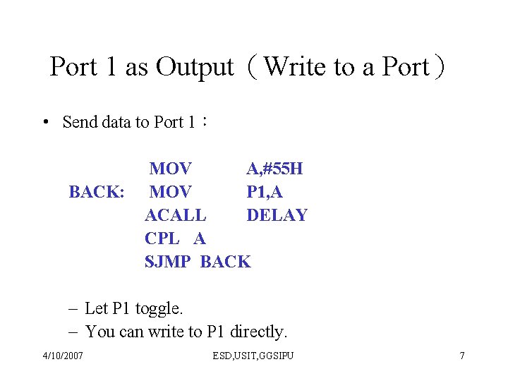
Port 1 as Output(Write to a Port) • Send data to Port 1: BACK: MOV A, #55 H MOV P 1, A ACALL DELAY CPL A SJMP BACK – Let P 1 toggle. – You can write to P 1 directly. 4/10/2007 ESD, USIT, GGSIPU 7

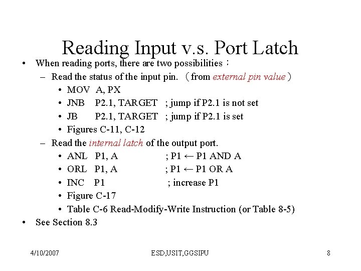
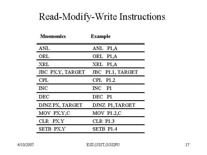
Reading Input v. s. Port Latch • When reading ports, there are two possibilities: – Read the status of the input pin. (from external pin value) • MOV A, PX • JNB P 2. 1, TARGET ; jump if P 2. 1 is not set • JB P 2. 1, TARGET ; jump if P 2. 1 is set • Figures C-11, C-12 – Read the internal latch of the output port. • ANL P 1, A ; P 1 ← P 1 AND A • ORL P 1, A ; P 1 ← P 1 OR A • INC P 1 ; increase P 1 • Figure C-17 • Table C-6 Read-Modify-Write Instruction (or Table 8 -5) • See Section 8. 3 4/10/2007 ESD, USIT, GGSIPU 8

Reading “High” at Input Pin Read latch 1. TB 2 write a 1 to the pin MOV P 1, #0 FFH Internal CPU bus 2. MOV A, P 1 Vcc external pin=High Load(L 1) D 1 Q 1 P 1. X pin P 1. X Write to latch Clk 0 Q M 1 TB 1 Read pin 3. Read pin=1 Read latch=0 Write to latch=1 4/10/2007 8051 IC ESD, USIT, GGSIPU 9

Reading “Low” at Input Pin Read latch 1. Vcc write a 1 to the pin 2. MOV A, P 1 TB 2 Load(L 1) external pin=Low MOV P 1, #0 FFH Internal CPU bus D 1 Q 0 P 1. X pin P 1. X Write to latch Clk Q 0 M 1 TB 1 Read pin 3. Read pin=1 Read latch=0 Write to latch=1 4/10/2007 8051 IC ESD, USIT, GGSIPU 10

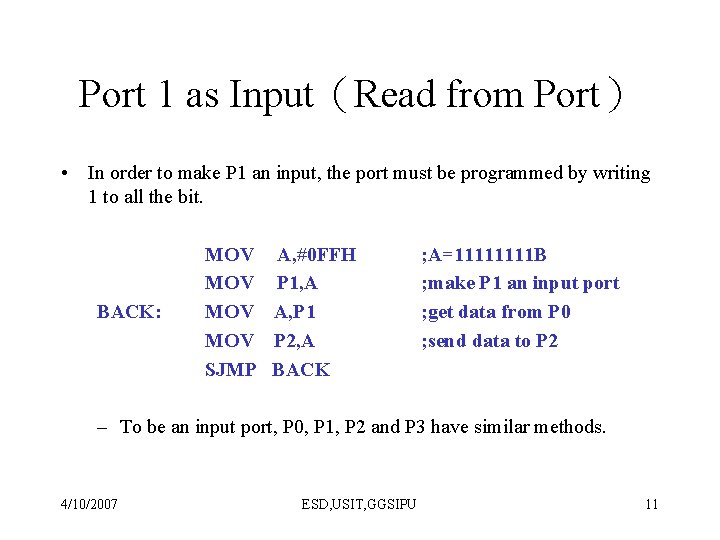
Port 1 as Input(Read from Port) • In order to make P 1 an input, the port must be programmed by writing 1 to all the bit. BACK: MOV MOV SJMP A, #0 FFH P 1, A A, P 1 P 2, A BACK ; A=1111 B ; make P 1 an input port ; get data from P 0 ; send data to P 2 – To be an input port, P 0, P 1, P 2 and P 3 have similar methods. 4/10/2007 ESD, USIT, GGSIPU 11

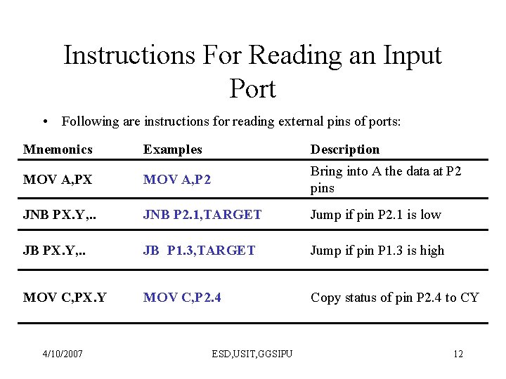
Instructions For Reading an Input Port • Following are instructions for reading external pins of ports: Mnemonics Examples Description MOV A, PX MOV A, P 2 Bring into A the data at P 2 pins JNB PX. Y, . . JNB P 2. 1, TARGET Jump if pin P 2. 1 is low JB PX. Y, . . JB P 1. 3, TARGET Jump if pin P 1. 3 is high MOV C, PX. Y MOV C, P 2. 4 Copy status of pin P 2. 4 to CY 4/10/2007 ESD, USIT, GGSIPU 12

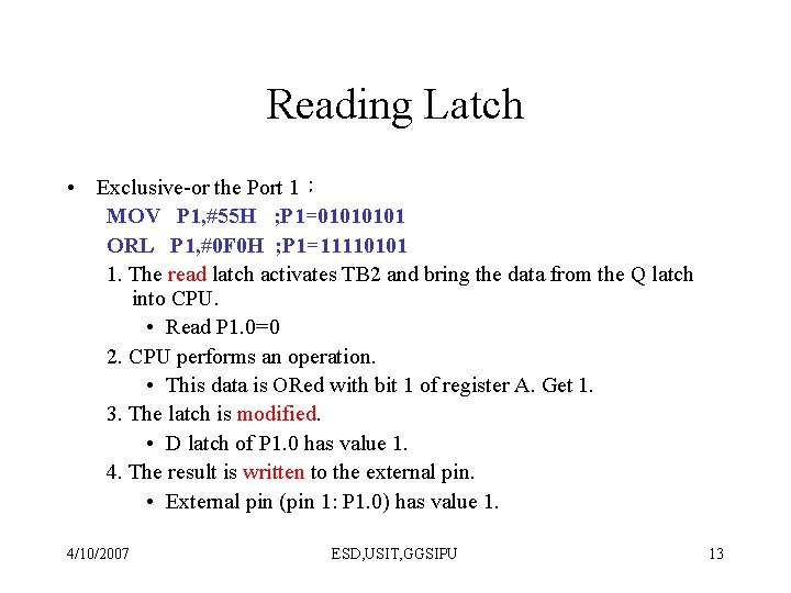
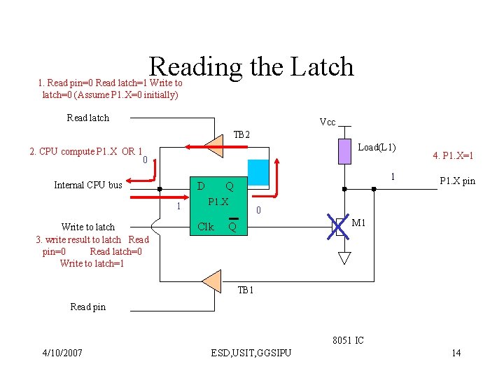
Reading Latch • Exclusive-or the Port 1: MOV P 1, #55 H ; P 1=0101 ORL P 1, #0 F 0 H ; P 1=11110101 1. The read latch activates TB 2 and bring the data from the Q latch into CPU. • Read P 1. 0=0 2. CPU performs an operation. • This data is ORed with bit 1 of register A. Get 1. 3. The latch is modified. • D latch of P 1. 0 has value 1. 4. The result is written to the external pin. • External pin (pin 1: P 1. 0) has value 1. 4/10/2007 ESD, USIT, GGSIPU 13

Reading the Latch 1. Read pin=0 Read latch=1 Write to latch=0 (Assume P 1. X=0 initially) Read latch Vcc TB 2 Load(L 1) 2. CPU compute P 1. X OR 1 0 Internal CPU bus D 1 Write to latch 3. write result to latch Read pin=0 Read latch=0 Write to latch=1 0 Q P 1. X Clk 1 4. P 1. X=1 P 1. X pin 0 M 1 Q TB 1 Read pin 8051 IC 4/10/2007 ESD, USIT, GGSIPU 14

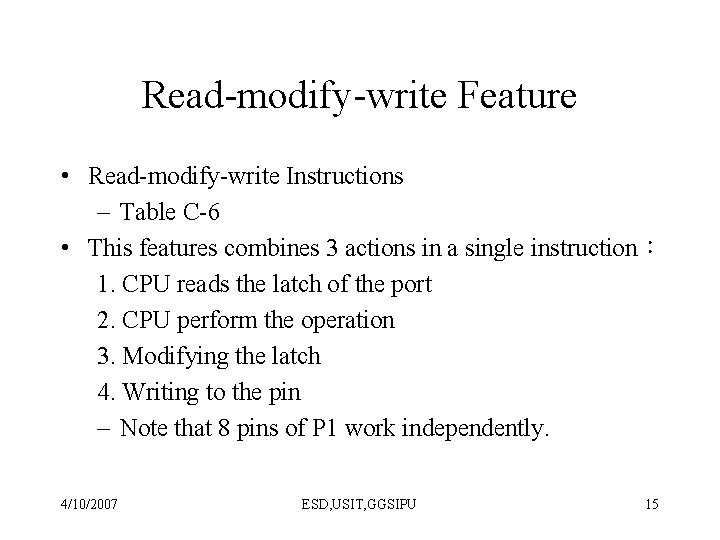
Read-modify-write Feature • Read-modify-write Instructions – Table C-6 • This features combines 3 actions in a single instruction: 1. CPU reads the latch of the port 2. CPU perform the operation 3. Modifying the latch 4. Writing to the pin – Note that 8 pins of P 1 work independently. 4/10/2007 ESD, USIT, GGSIPU 15

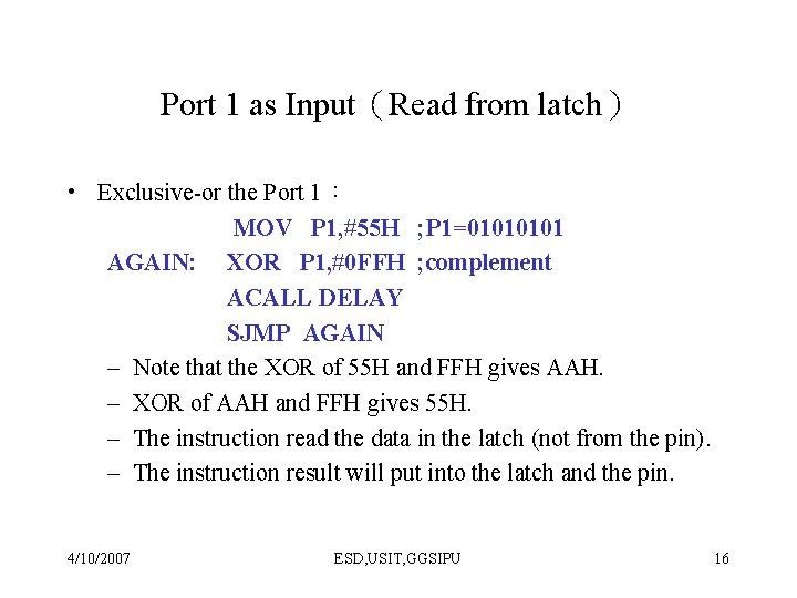
Port 1 as Input(Read from latch) • Exclusive-or the Port 1: MOV P 1, #55 H ; P 1=0101 AGAIN: XOR P 1, #0 FFH ; complement ACALL DELAY SJMP AGAIN – Note that the XOR of 55 H and FFH gives AAH. – XOR of AAH and FFH gives 55 H. – The instruction read the data in the latch (not from the pin). – The instruction result will put into the latch and the pin. 4/10/2007 ESD, USIT, GGSIPU 16

Read-Modify-Write Instructions Mnemonics 4/10/2007 Example ANL P 1, A ORL P 1, A XRL P 1, A JBC PX. Y, TARGET JBC P 1. 1, TARGET CPL P 1. 2 INC DEC P 1 DJNZ PX, TARGET DJNZ P 1, TARGET MOV PX. Y, C MOV P 1. 2, C CLR PX. Y CLR P 1. 3 SETB PX. Y SETB P 1. 4 P 1 ESD, USIT, GGSIPU 17

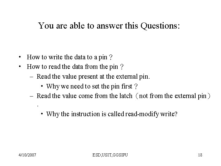
You are able to answer this Questions: • How to write the data to a pin? • How to read the data from the pin? – Read the value present at the external pin. • Why we need to set the pin first? – Read the value come from the latch(not from the external pin). • Why the instruction is called read-modify write? 4/10/2007 ESD, USIT, GGSIPU 18

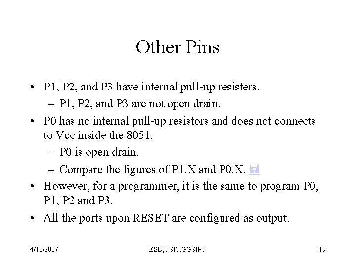
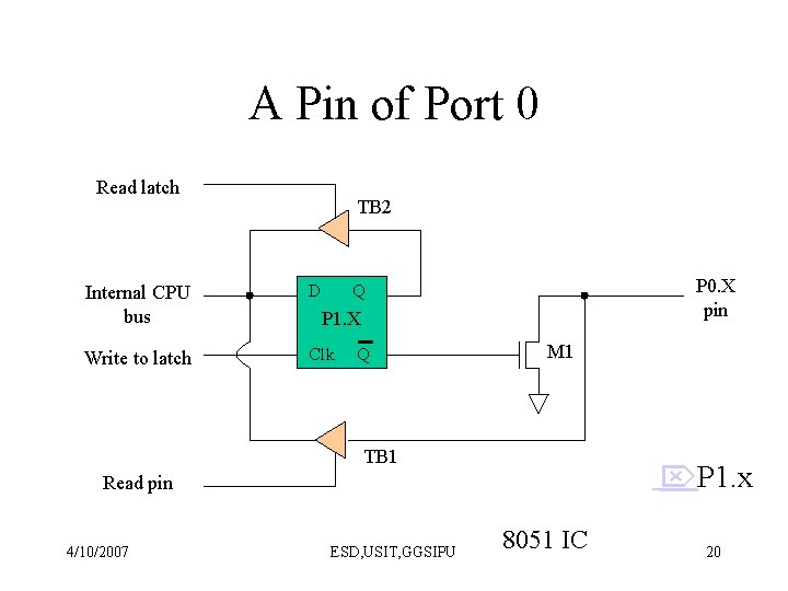
Other Pins • P 1, P 2, and P 3 have internal pull-up resisters. – P 1, P 2, and P 3 are not open drain. • P 0 has no internal pull-up resistors and does not connects to Vcc inside the 8051. – P 0 is open drain. – Compare the figures of P 1. X and P 0. X. • However, for a programmer, it is the same to program P 0, P 1, P 2 and P 3. • All the ports upon RESET are configured as output. 4/10/2007 ESD, USIT, GGSIPU 19

A Pin of Port 0 Read latch TB 2 Internal CPU bus D Write to latch Clk P 0. X pin Q P 1. X Q M 1 TB 1 P 1. x Read pin 4/10/2007 ESD, USIT, GGSIPU 8051 IC 20

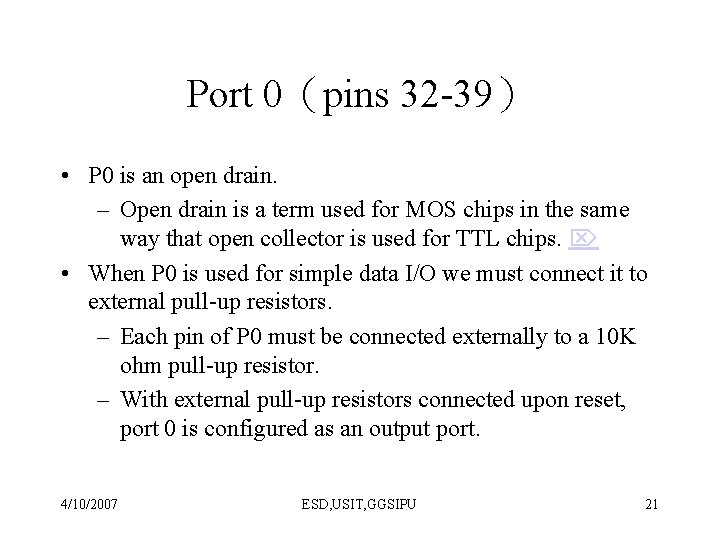
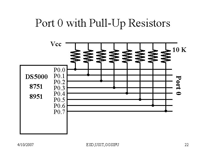
Port 0(pins 32 -39) • P 0 is an open drain. – Open drain is a term used for MOS chips in the same way that open collector is used for TTL chips. • When P 0 is used for simple data I/O we must connect it to external pull-up resistors. – Each pin of P 0 must be connected externally to a 10 K ohm pull-up resistor. – With external pull-up resistors connected upon reset, port 0 is configured as an output port. 4/10/2007 ESD, USIT, GGSIPU 21

Port 0 with Pull-Up Resistors Vcc 10 K 4/10/2007 Port 0 P 0. 0 DS 5000 P 0. 1 P 0. 2 8751 P 0. 3 P 0. 4 8951 P 0. 5 P 0. 6 P 0. 7 ESD, USIT, GGSIPU 22

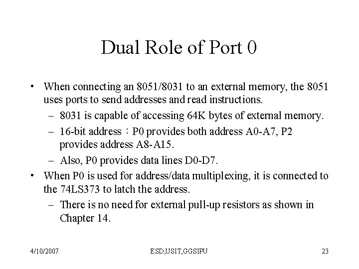
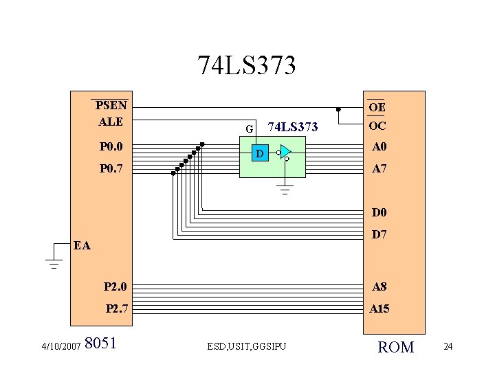
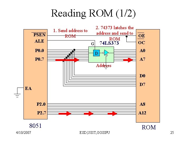
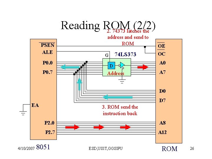
Dual Role of Port 0 • When connecting an 8051/8031 to an external memory, the 8051 uses ports to send addresses and read instructions. – 8031 is capable of accessing 64 K bytes of external memory. – 16 -bit address:P 0 provides both address A 0 -A 7, P 2 provides address A 8 -A 15. – Also, P 0 provides data lines D 0 -D 7. • When P 0 is used for address/data multiplexing, it is connected to the 74 LS 373 to latch the address. – There is no need for external pull-up resistors as shown in Chapter 14. 4/10/2007 ESD, USIT, GGSIPU 23

74 LS 373 PSEN ALE P 0. 0 74 LS 373 G D P 0. 7 OE OC A 0 A 7 D 0 D 7 EA 4/10/2007 P 2. 0 A 8 P 2. 7 A 15 8051 ESD, USIT, GGSIPU ROM 24

Reading ROM (1/2) P 0. 0 2. 74373 latches the address and send to OE ROM OC G 74 LS 373 A 0 P 0. 7 A 7 PSEN ALE 1. Send address to ROM D Address D 0 D 7 EA P 2. 0 A 8 P 2. 7 A 12 8051 4/10/2007 ESD, USIT, GGSIPU ROM 25

Reading ROM (2/2) 2. 74373 latches the PSEN ALE P 0. 0 P 0. 7 address and send to ROM 74 LS 373 G D Address OE OC A 0 A 7 D 0 D 7 EA 4/10/2007 3. ROM send the instruction back P 2. 0 A 8 P 2. 7 A 12 8051 ESD, USIT, GGSIPU ROM 26

ALE Pin • The ALE pin is used for de-multiplexing the address and data by connecting to the G pin of the 74 LS 373 latch. – When ALE=0, P 0 provides data D 0 -D 7. – When ALE=1, P 0 provides address A 0 -A 7. – The reason is to allow P 0 to multiplex address and data. 4/10/2007 ESD, USIT, GGSIPU 27

Port 2(pins 21 -28) • Port 2 does not need any pull-up resistors since it already has pull-up resistors internally. • In an 8031 -based system, P 2 are used to provide address A 8 -A 15. 4/10/2007 ESD, USIT, GGSIPU 28

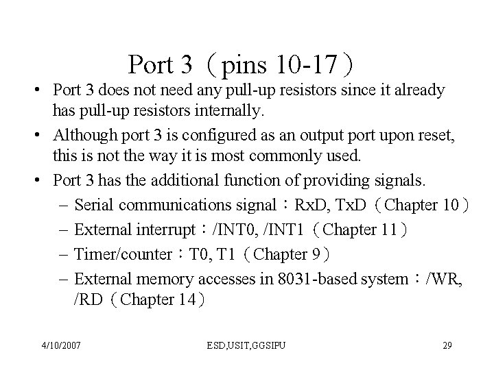
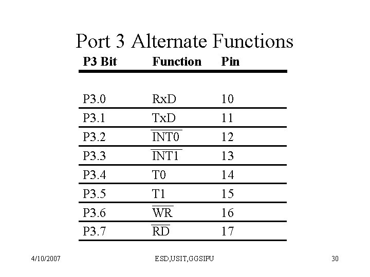
Port 3(pins 10 -17) • Port 3 does not need any pull-up resistors since it already has pull-up resistors internally. • Although port 3 is configured as an output port upon reset, this is not the way it is most commonly used. • Port 3 has the additional function of providing signals. – Serial communications signal:Rx. D, Tx. D(Chapter 10) – External interrupt:/INT 0, /INT 1(Chapter 11) – Timer/counter:T 0, T 1(Chapter 9) – External memory accesses in 8031 -based system:/WR, /RD(Chapter 14) 4/10/2007 ESD, USIT, GGSIPU 29

Port 3 Alternate Functions 4/10/2007 P 3 Bit Function Pin P 3. 0 P 3. 1 P 3. 2 P 3. 3 P 3. 4 P 3. 5 P 3. 6 P 3. 7 Rx. D Tx. D INT 0 INT 1 T 0 T 1 WR RD 10 11 12 13 14 15 16 17 ESD, USIT, GGSIPU 30