INVERTER Inverter produces a complete range of logic


 0. 8 VDD D IDS C 0. 5 VDD Vgs (dep) = 0")
 Ids starts")


 Reduce Vth we have to larger K in order to bring K ,")
 Vdep - mode negative, will increase current driving, K es More as")


- Slides: 21
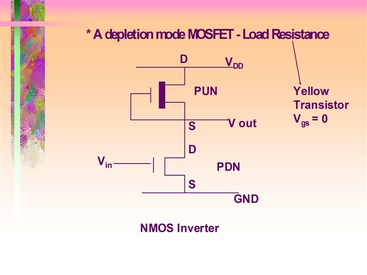
INVERTER : • Inverter - produces a complete range of logic circuits • Restoring logic levels VD • NAND & NOR gates D Load Resistor P. U. R O/P I/P S GND
RESISTANCE PULLUP • DEPLETION MODE PULLUP ==RP. U • ENHANCEMENT PULLUP ==R P. U • PMOS PULLUP •
NMOS Inverter Transfer Characteristic • If O/P current = O Ids dep = Ids enh. • Depletion MOSFET Gate connected to source - always on - Vgs = O is the relevant curve. • Dep T 1 - Pull-up (P. U) • Enh T 2 - Pull -down (P-D)
• Inverter tr. ch Superimpose Vgs = O dep m family of curves on enh. mode Vdep (min) = Venh (max)
Vgs(enh) 0. 8 VDD D IDS C 0. 5 VDD Vgs (dep) = 0 NMOS Inverter Transfer Characteristic B 0. 4 VDD A 0. 2 VDD Vgs (enh) = Vin Vds (enh) 0 = VDD - Vds (dep) = Vout 0. 5 VDD Vds (enh) VDD
• As Vin = Vgs P. d > Vt (p. d) Ids starts flowing O/P Vout = Vds (dep) P. U starts reduc • As Vin - is more P. d - Saturation • During Transition Slope of Tr-ch = Gain
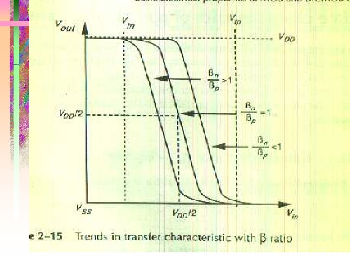
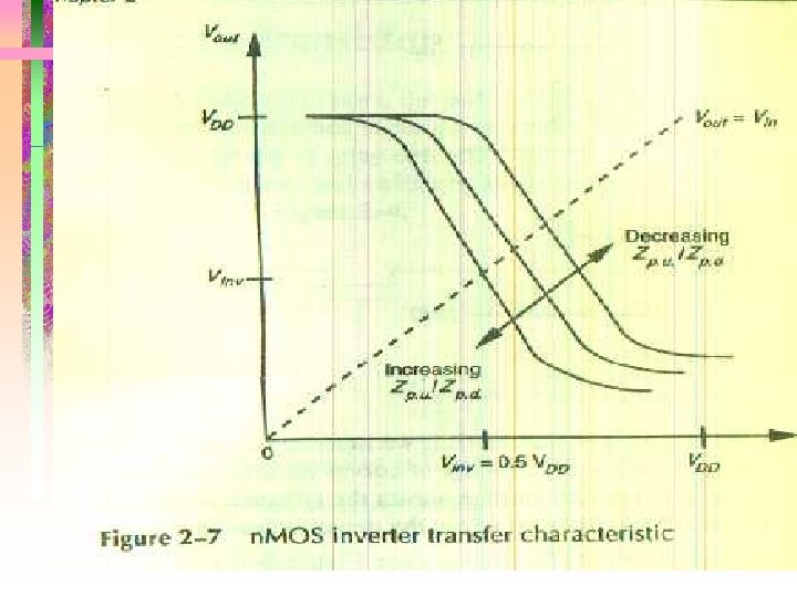
• Point at which Vin = Vout = Vin V. Vin. V can be shifted by varying Z P. u / Z P. d Z = L/W of MOSFET
VDD x Zp. d Vol = Zp. u + Zp. d Rinv=ZP. D/ZP. U Vol VDD = 1+ Zp. d/ Zp. u
NMOS Inverter Vdd Z=2/1 Zp. u Region 2 Vdd W 20 K Lin W 40 K Sat Vout Z=1/2 Vout Zp. d W 5 K GND
Vi. H Vdd A Rinv Tesed Vol Becomes Smaller B Vinv VOL VIH VIL Vin = (1) Vout. Vol = VDD p. v Sat 9 C Vo = VDD p. u. Linear 5 (2) When Vin = 1 D O/P = Low E P. V Sat P. D Linear Vinv VIH Vdd Region D RINV = zp. u/ zp. d = 40/5 NON ZERO OUTPUT
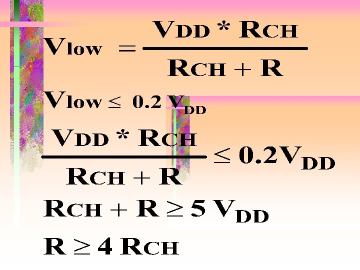
Discussion on NMOS Inverter with pull up using depletion Mode to ‘R’ Pull - C Vdd Transistor compared. Vdd Vgs = 0 DEP R Vout T Vin GND GND 5 V Process P. U. R = 40 K IP. V = 125 µA P. V. R function - limit the pull up current to some fraction of P. D. current
Ratioed Logic RC > Rch C P. U. Time > Pull down time A symmetry of S/wing time RATIOED LOGIC Speed Improve (1) R - Small - Rch - Small (W large Si area More Power Dissipation = (Vdd - V 10)2/R (2) R can be lowered to attain high speed or Vth can be lowered
DEP NOD P. U ‘C’ Point. Equating Sat. currents
(1) Reduce Vth we have to larger K in order to bring K , Large - Assymmetry large-- t charge & t discharge
2) Vdep - mode negative, will increase current driving, K es More as
SUMMARY INVERTER • RESISTANCE -DIFFICULT TO FABRICATE -LARGE AREA • DEPLETION MODE • DISSIPATION IS HIGH • 1 TO 0 TRANSITION AFTER VIN > VTN • 1 TO 0 TRANSITION -P. U IS NON SATURATED DISCHARGING TAKES A LONGER TIME.
• ENHANCEMENT LOAD OR PULLUP: • DISSIPATION IS HIGH • V -OUT < VDD